Transcription
Fundamentals ofLow-Noise Analog Circuit DesignW. MARSHALL LEACH, JR., SENIOR MEMBER, IEEEThis paper presents a tutorial treatment of the fundamentals ofnoise in solid-state analog electronic circuits. It is written for upperdivision students andpracticing engineers who wish to gain a basicknowledge of the theory of electronic noise and techniques forlow-noise circuit design. The paper presents an overview of noisefundamentals, a description of noise models for passive devicesand active solid-state devices, methods of calculating the noiseperformance of ampl ers, and techniques for minimizing noisein circuit design. The theory and methods are applicable to bothdiscrete and integrated circuits.I. INTRODUCTIONWith modem solid-state devices and integrated circuits,it is possible to realize amplifiers that exhibit an extremelyhigh voltage gain. Indeed, a gain of almost any desiredmagnitude can be obtained by cascading stages. This mightseem to imply that an arbitrarily small signal can beamplified to any desired level. This is not true because thereis always a limit to the smallest signal that can be amplified.This limit is determined by electronic noise. If a signal isso small that it is masked by the noise in an amplifier, it isimpossible to recover the signal by amplification.Noise is present in all electronic circuits. It is generatedby the random motion of electrons in a resistive material,by the random recombination of holes and electrons ina semiconductor, and when holes and electrons diffusethrough a potential barrier. The theoretical basis for theanalysis of noise lies in the areas of semiconductor devicephysics and probability theory [ 11-[3]. The circuit designercan easily be intimidated by some of this theory. For thisreason, low-noise circuit design is perceived by some asbeing an esoteric area. However, it can be straightforwardif the device noise models are understood. These modelsare quite simple and no special knowledge of semiconductordevice physics or probability theory is required to use them.This paper gives a tutorial introduction to the subjectof noise in analog electronic circuits. The material isapplicable to both discrete and integrated circuits. Theprincipal sources of noise are described and models for theManuscript received January 28, 1993; revised March 29, 1994.The author is with Georgia Institute of Technology, School of Electricaland Computer Engineering, Atlanta, Georgia 30332-0250 USA.IEEE Log Number 9404667.sources are given. The general characteristics of noise aredescribed and methods for its measurement are discussed.Noise models for the bipolar junction transistor (BJT) andthe field-effect transistor (FET) are given. These devices areanalyzed by reflecting all noise sources into an equivalentnoise voltage in series with the device input. The conditions for minimum noise in each are derived. To illustratethe principles, a design example is presented where thetheoretically predicted noise performance is compared tothat predicted by a SPICE simulation.The notations for voltages and currents correspond tothe following conventions: dc quantities are indicated byan upper case letter with upper case subscripts, e.g., IC,I o , etc. Small-signal ac quantities are indicated by a lowercase letter with lower case subscripts, e.g., us, it, etc. Rootmean square (rms) or effective values are indicated by anupper case letter with lower case subscripts, e.g., V,, It, etc.Phasor quantities are indicated by a bold-face upper caseletter and bold face lower case subscripts, e.g., V,,I t , etc.Circuit symbols for independent sources are circular andthose for controlled sources have a diamond shape. Voltagesources have a f sign within the symbol and currentsources have an arrow. Noise sources are representedas independent sources having a smaller circular symbolthan signal sources. In the numerical evaluation of noiseequations, the following values are used: Boltzmann’sconstant IC 1.38 xJ/K, absolute temperatureT 300 K, electronic charge q 1.60 x 1O-l’ C , andthermal voltage VT 0.0259 V.11. THERMAL NOISEA noise voltage called thermal noise is generated whenthermal energy causes free electrons to move randomlyin a resistive material [ 2 ] , [4],[ 5 ] . The phenomenon wasdiscovered (or anticipated) by Schottky in 1928 and firstmeasured and evaluated by Johnson in the same year. It isalso referred to as Johnson noise. Shortly after its discovery,Nyquist used a thermodynamic argument to show that theopen-circuit rms thermal noise voltage across a resistor isgiven by0018-9219/94 04.00 0 1994 IEEELEACH: FUNDAMENTALS OF LOW-NOISE ANALOG CIRCUIT DESIGN1515
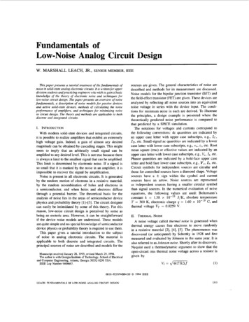
PAI1(a)(b)(a)(b)Fig. 1. (a) Thevenin noise model of resistor. (b) Norton noisemodel of resistor.Fig. 2. (a) Parallel RC network. (b) Single pole RC low-passfilter.where IC is Boltzmann's constant, T is the absolute temperature, R is the resistance, and A f is the bandwidth in hertzover which the noise is measured.The power in thermal noise is proportional to the squareof Vt which is independent of frequency for a fixed bandwidth. The power between 100 and 200 Hz is the same asit is between 10100 and 10200 Hz. Such noise is said tohave a uniform orflat power distribution and is called whitenoise. It is called this by analogy to white light which alsohas a flat power distribution in the optical band.Equation (1) is the basis for two resistor noise models-the Thevenin model and the Norton model. These areshown in Fig. 1. The short-circuit rms thermal noise currentin the Norton model of Fig. l(b) is given bybe modeled by a Gaussian or normal probability-densityfunction. For a Gaussian random variable, the probabilityBecause noise is random, the source polarities in the figureare arbitrary. In general, the polarities must be labeled whenwriting circuit equations. The total rms noise in a circuit isindependent of the assumed polarities.Thermal noise is present in all circuit elements containingresistance. The noise is independent of the composition ofthe resistance. It is modeled the same way in discrete-circuitresistors and in integrated-circuit monolithic and thin-filmresistors [4]. A carbon composition resistor generates thesame amount of thermal noise as a metal film resistor of thesame value. However, an additional noise component calledflicker noise may be present in the carbon compositionresistor. It results from the variable contact between thecarbon particles of the resistive material. This noise ispresent only when a direct current flows in the resistor.It is discussed in more detail in Section IV.Equation (1) shows that thermal noise voltage is proportional to the square root of the product of the absolutetemperature, the resistance value, and (to the highest measurable frequencies) the bandwidth over which the noiseis measured. For a fixed temperature, the thermal noisevoltage in a circuit can be reduced by minimizing theresistance and the bandwidth. Further reduction can onlybe obtained by operating the circuit at lower temperatures.The crest factor for thermal noise is defined as the ratioof the peak value to the rms value. Although the rmsvalue can be calculated, the peak value cannot becauseit is random. A common definition for the peak value isthe level that is exceeded only 0.01% of the time [5].To relate this to the rms value, a statistical model forthe amplitude distribution is required. It is common toassume that the amplitude distribution of thermal noise can1516that the instantaneous value exceeds four times the rmsvalue is approximately 0.01%. Thus the crest factor isapproximately 4.In any circuit containing resistors, capacitors, and inductors, only the resistors generate thermal noise. (Thewinding resistance of an inductor must be modeled as aseparate resistor.) Let 2 be the complex impedance of atwo-terminal network. The open-circuit rms thermal noisevoltage generated by the network in the frequency bandfrom f l to f 2 is given bywhere Re ( 2 )is the real part of 2 and f is the frequencyin hertz. Let f 2 f i Af. If A f is sufficiently small, thenoise voltage divided by the square root of the bandwidthcan be solved for to obtain (4)This equation defines what is called the spot noise voltagegenerated by the impedance. The units are read "volts perroot hertz".The total noise voltage generated by any resistor islimited by its shunt capacitance. For a physical resistor,this capacitance can never be zero. Figure 2(a) shows aparallel RC circuit. The complex impedance and its realpart, respectively, are given by2 Rll(l/j27rfC) R/(1 j 2 7 r f R C )andRe(2) R / [ l (27rfRC)'I.It follows from (3) that the total rms open-circuit thermalnoise voltage is given byIt can be concluded that the total noise voltage generatedby a resistor is a function only of the temperature and thetotal shunt capacitance across the resistor.PROCEEDINGS OF THE IEEE. VOL. 82, NO. IO. OCTOBER 1994
111. SHOTNOISEShot noise is generated when a current flows across apotential barrier [l], [4], [5]. It is caused by the randomfluctuation of the current about its average value and occursin vacuum tubes and in semiconductor devices. In vacuumtubes, it is generated by the random emission of electronsfrom the cathode. In semiconductors, it is generated bythe random diffusion of holes and electrons through a p-njunction and by the random generation and recombinationof hole-electron pairs.The shot noise generated by a device is modeled by aparallel noise current source. The rms shot-noise current inthe frequency band Af is given byIsh J24lafby the application of too large an input voltage. A diodein parallel with the base-to-emitter junction is often usedto prevent it. For example, the MAT-02 and MAT-03 lownoise matched dual monolithic BJT pairs have the diodesfabricated as part of the devices.The power in flicker noise is proportional to the squareof I f which is inversely proportional to the frequency.Because of this, flicker noise is commonly referred to asl/f noise, read “one-over-f noise.” Because it increasesat low frequencies, it is also referred to as low-frequencynoise. Another name that is sometimes used is pink noise[lo]. This name comes from the optical analog of pinklight which has a power density that increases at the longerwavelengths, i.e., at the lower frequencies.(6)where q is the electronic charge and I is the dc currentflowing through the device. This equation was derived byShottky in 1928 and is known as the Shottky formula.For a fixed bandwidth, the noise current is independent offrequency so that shot noise has a flat power distribution,i.e., it is white noise. It is commonly assumed that theamplitude distribution of shot noise can be modeled bya Gaussian or normal distribution. Therefore, the relationbetween the crest factor and rms value for shot noise is thesame as it is for thermal noise.IV. FLICKERNOISEThe imperfect contact between two conducting materialscauses the conductivity to fluctuate in the presence of adc current [4], [5]. This phenomenon generates what iscalled Jicker noise or contact noise. It occurs in any devicewhere two conductors are joined together, e.g., the contactsof switches, potentiometers, relays, etc. In resistors, it iscaused by the variable contact between particles of theresistive material and is called excess noise [6]. Metal filmresistors generate the least excess noise, carbon compositionresistors generate the most, with carbon film resistors lyingbetween the two. Flicker noise in BJT’s occurs in the basebias current. In FET’s, it occurs in the drain bias current.Flicker noise is modeled by a noise current source inparallel with the device. The rms flicker noise current inthe frequency band Af is given byV. BURSTNOISEBurst noise is caused by a metallic impurity in a p-njunction [4], [5], [6]. Because it is caused by a manufacturing defect, it is minimized by improved fabricationprocesses. When burst noise is amplified and reproducedby a loudspeaker, it sounds like corn popping. For thisreason, it is also called popcom noise. When viewed on anoscilloscope, burst noise appears as fixed-amplitude pulsesof randomly varying width and repetition rate. The rate canvary from less than one pulse per minute to several hundredpulses per second. Typically, the amplitude of burst noiseis 2 to 100 times that of the background thermal noise [5].Burst noise in BJT’s is discussed in [ 113 and [ 121.VI. NOISEBANDWIDTHWhen a noise voltage is measured, the observed valueis dependent on the bandwidth of the measuring voltmeterunless a filter is used to limit the bandwidth to a value thatis less than that of the voltmeter. It is common to use such afilter in making noise measurements. The noise bandwidthof a filter is defined as the bandwidth of an ideal filter whichpasses the same rms noise voltage as the filter, where theinput signal is white noise [5], [6]. The filter and the idealfilter are assumed to have the same gains.To express the noise bandwidth of a filter analytically,let A ( f ) be its voltage gain transfer function and let A0 bethe maximum value of [ A (f)I, where f is the frequency inhertz. The noise bandwidth B in hertz is given by(7)where I is the dc current, n N 1, K f is the flickernoise coefficient, and m is the flicker-noise exponent. Inmodeling J E T noise at low temperatures, n is not fixed[7]. In modeling base-current flicker noise in the BJT, mis typically in the range 1 m 3 [ti]. To simplify theanalyses in the following, it is assumed that n m 1 inall flicker-noise equations. It is straightforward to modifythe results for other values of n and m.In BJT’s, flicker noise can increase significantly if thebase-to-emitter junction is subjected to reverse breakdown[9]. This can be caused during power supply turn-on orLEACH: FUNDAMENTALS OF LOW-NOISE ANALOG CIRCUIT DESIGNThis equation is interpreted graphically in Fig. 3 for both alow-pass filter and a band-pass filter. In each case, the actualfilter response and the response of an ideal filter having thesame noise bandwidths are shown. For the noise bandwidthsto be the same, the area under the actual filter curve mustbe equal to the area under the ideal filter curve. For thelow-pass case, this makes the two indicated areas equal. Asimilar interpretation holds for the band-pass case.There are two classes of low-pass filters which are oftenused in making noise measurements. The first has n realpoles, all with the same frequency. The second is an n1517
Fig. 3. Graphical interpretation of noise bandwidth for low-passand band-pass filters.Table 1. Noise Bandwidth E of Low-Pass FiltersNumberof PolesSlopedB/decReal PoleButterworthEBpole Butterworth filter. Table 1 gives the noise bandwidthB for each filter as a function of the number of poles nfor 1 5 TI 5 5. For the real-pole filter, the noise bandwidthis given as a function of both the pole frequency f o andthe upper -3-dB cutoff frequency f3. For the Butterworthfilter, the noise bandwidth is given as a function of theupper -3-dB frequency. The table shows that the noisebandwidth approaches the -3-dB frequency as the numberof poles is increased.A simple R C low-pass filter such as the one shown inFig. 2(b) is an example single-pole filter that is often usedto limit the bandwidth of noise. This filter has the transferfunction A( f ) 1/(1 j27r f R C ) . The pole frequency isf o 1/27rRC. From Table 1, the noise bandwidth is givenby B 1.571/27rRC 1/4RC.Band-pass filters are used in making spot noise measurements. The filter bandwidth must be small enough sothat the input noise voltage as a function of frequency isapproximately constant over the filter bandwidth. The spotnoise voltage is obtained by dividing the filter noise outputvoltage by the square root of its noise bandwidth. A filterthat is often used for these measurements is a second-orderband-pass filter. Such a filter has a -3-dB bandwidth offc/Q, where f c is the center frequency and Q is the qualityfactor. The noise bandwidth is given by B 7r fc/2Q. Thisis greater than the -3-dB bandwidth by the factor / 2 .A single-pole high-pass filter cascaded with a singlepole low-pass filter is a special case of a band-pass filterhaving two real poles. Let the pole frequency of the highpass filter be denoted by f l and that of the low-pass filterbe denoted by f 2 . The center frequency and the qualityfactor of the band-pass filter are given by f c (f1f2)lI2and Q f c / ( f lf 2 ) . The noise bandwidth is given byB 7rfc/2Q 7r( f l f 2 ) / 2 . (Note that the frequencies fland f 2 are not the -3-dB frequencies of the filter. If the -3- 1518dB frequencies are denoted by f a and f b , where f b f a ,the quality factor is also given by Q f c / ( f b - fa).Thus an alternate expression for the noise bandwidth isB T ( f b - fa)/2. The noise bandwidth of any filter can be measuredif a white-noise source and another filter with a knownnoise bandwidth are available. With both filters drivensimultaneously by the white-noise source, the ratio of thenoise bandwidths is equal to the square of the ratio ofthe output voltages. If VI is the rms noise output voltagefrom a filter with the known noise bandwidth B1 andV2 is the rms noise output voltage from a filter with theunknown noise bandwidth B2, it follows that Bz is givenby B2 B1(V2/Vd2.VII. MEASURINGNOISENoise is normally measured at an amplifier output wherethe voltage is the largest and easiest to measure [ 5 ] , [61,[lo]. The output noise is referred to the input by dividingby the gain. In measuring individual devices, a test fixturecan be used to hold the gain constant by use of negativefeedback [13]. The measuring voltmeter should have abandwidth that is at least ten times the noise bandwidth ofthe circuit being measured [5]. If the voltmeter bandwidthis insufficient, a filter with a known noise bandwidth canbe used preceding the voltmeter to limit the bandwidth toa known value.The voltmeter crest factor is the ratio of the peak inputvoltage to the full-scale rms meter reading at which theintemal meter circuits overload. For a sine-wave signal, theminimum voltmeter crest factor isFor noise measurements, a higher crest factor is required. For Gaussian noise,a crest factor of 3 gives an error less than 1.5%. A crestfactor of 4 gives an error less than 0.5%.To minimize errorscaused by an inadequate crest factor, measurements shouldbe made on the lower one-third to one-half of the voltmeterscale to avoid overload on the noise peaks.A true rms voltmeter is preferred over one which responds to the average reqtified value of the input voltagebut has a scale calibrated to read rms. When the latter typeof voltmeter is used to measure noise, the reading will below. For Gaussian noise, the reading can be corrected bymultiplying the measured voltage by 1.13.Fairly accurate rms noise measurements can be madewith an oscilloscope [14]. A filter must be used to limitthe noise bandwidth at its input. Although the procedure issubjective, the rms voltage can be estimated by dividing theobserved peak-to-peak voltage by the crest factor [5]. Oneof the advantages of using the oscilloscope is that nonrandom noise which can affect the measurements can beidentified, e.g., a 60-Hz hum signal.One method is to display the noise simultaneously onboth vertical channels of a dual-channel oscilloscope thatis set in the dual-sweep mode. The two channels must beidentically calibrated and the sweep rate must not be set toohigh. The vertical offset between the two traces is adjusteduntil the dark area between them just disappears. The rmsa.PROCEEDlNGS OF TKE IEEE, VOL. 82, NO. 10, OCTOBER 1994
a7The phasor output voltage V , is solved for by settingV V - to obtainvO"t3VO-Vt2 IVt2R 2 R3)Cv, Vtl 1 j1 (jwR2CQR 3 Vt3v-This expression is converted into a root-square sum bytaking the square root of the sum of the squared magnitudesas follows:(b)(a)Fig. 4. Circuits used to illustrate addition of noise voltages." 1 w2(R2 R3)'C21 W2R372noise voltage is then measured by grounding the two inputsand reading the vertical offset between the traces [15].VIII. ADDITIONOF NOISEVOLTAGES If the models for all noise sources are known, thenoise output voltage of a circuit can be calculated by themethods of linear circuit analysis. The output voltage isfirst calculated as if the instantaneous time-domain valueof each source is known. The rms value is then obtainedby converting the expression into a root-square sum.To illustrate this, consider the circuit of Fig. 4(a) consisting of an ideal noiseless operational amplifier (op-amp) andthree resistors. Each resistor is modeled by its Theveninnoise model, where the source polarity is arbitrary. LetRE RI R2 R3. The instantaneous op-amp inputvoltages are given by v vti(R2 R3)/Rc (ut2 ut3 vo)Ri/RcandU- (uti - vt2)R3/RC ( 3vo)(Ri Rz)/Rc.The instantaneous output voltage is obtained by settingU w- to obtain v, vtlwt2(R1 R 3 ) / R 2- vt3. Therms value of v, is obtained by converting the expressioninto a root-square sum by taking the square root of the sumof the squares as follows: [licT(R1 (Ri R3)'R2 R3) AS] 1'2(9)where the instantaneous voltages have been replaced bythe rms voltages. In squaring each term, all negative signsdisappear so that the result is independent of the sourcepolarities.The preceding example illustrates noise calculationswhen complex impedances are not involved. The circuit ofFig. 4(b) is an example circuit with a complex impedance.The circuit equations are written as if the noise voltageswere phasor quantities which are denoted here by bold faceletters. Let Z1 R2 R3 l/jwC and 2 2 R2 l/jwC,where w 2 n f . The op-amp phasor input voltages aregiven V Vtl and V - Vt2R3/Z1 (Vt3 Vo)22/Z1. LEACH: FUNDAMENTALS OF LOW-NOISE ANALOG CIRCUIT DESIGN[,,,(R1 W2(R2 R3)2C21 w2R2C2 R2 1 Ww2R;C22R'C2 R s ) A f ](11)where the phasor voltages have been replaced by rmsvoltages. This expression is a function of frequency. Toevaluate the noise voltage over a band, A f is replaced bydf and the quantity inside the brackets integrated over theband. Alternately, the expression can be converted into aspot noise voltage by dividing both sides byIn the examples presented above, two simplifying assumptions are made. First, it is assumed that the opamps are noiseless. This is not true for physical op-amps.Second, it is assumed that the noise sources are statisticallyuncorrelated. This assumption is valid when the noisesources are independent of each other, e.g., when each noisesource represents the noise generated by a separate resistor.m.I x . THE vn-I, AMPLIFIERNOISEMODELThe noise output from any amplifier is a function of thenoise generated by the source and the noise generated insidethe amplifier. An amplifier noise model can be obtained byreflecting all internal noise sources to the input. In orderfor the reflected sources to be independent of the sourceimpedance, two noise sources are required-a series voltagesource w, and a shunt current source in [16].Figure 5(a) shows the amplifier noise model, where v,is the instantaneous source voltage, Rs is the source resistance, and vts is the instantaneous thermal noise voltagegenerated by Rs. The instantaneous output voltage is givenbywhere A is the voltage gain and R; is the input resistance.The equivalent noise input voltage is the voltage in serieswith the amplifier input that generates the same noisevoltage at the output as all noise sources in the circuit.It is denoted by U,; and is given by the sum of the noiseterms in the parentheses in (12).1519
measure I,, V,, is measured with a large value resistorfor Rs (ideally Rs 00) and I , is calculated from(17). In measuring V,,, it is common to use a filter witha known noise bandwidth preceding the voltmeter. Themeasurements can be converted to spot-noise values bydividing by the square root of the filter noise bandwidth.x. THE SIGNAL-TO-NOISERATIOThe decibel signal-to-noise ratio (SNR) of the amplifierof Fig. 5(a) is defined by[SNR 2010g -(c)(b)Fig. 5. (a) \;-I,, amplifier noise model. (b) Source with shuntresistor across output. (c) Thevenin equivalent circuit of sourceand shunt resistor. 101ogThe rms value of v,; is obtained by taking the squareroot of the time average of v ,('u, i,Rs) U: v,i,Rs i:Rg. 2 i ut",Because the noise generated by Rs is independent of thenoise generated by the amplifier, the average value of theterm uts (U, in Rs) is zero. However, it cannot be assumedthat the average value of w,i, is zero. This is because oneor more noise sources in the amplifier might contribute toboth w, and in. In this case, the correlation coefficient pbetween w, and i, must be known. This is defined by1P(13)-(.nin)VnInwhere (vain)represents the time average ofvalue of wni is then given byV,, \/41cTRsAfTJ, ,.The rms V: 2pV,I,Rs I:Rg.1721"S 2pV,I,Rs I;Rg]'14kTRsA.f V:(18)The source resistance which maximizes the SNR is Rs 0.Although the source resistance is normally fixed, it can beconcluded that a series resistor should not be connectedbetween a source and an amplifier if noise performance isa design criterion.Figure 5(b) shows a source with a shunt resistor connected across its output terminals. To investigate the effectof this resistor on noise, a Thevenin equivalent circuit ofthe source and shunt resistor is first made. The circuit isshown in Fig. 5(c), where v t l is the instantaneous thermalnoise voltage generated by the effective source resistanceRsllR1. With this circuit connected to the amplifier input in Fig. 5(a), it follows by analogy to (12) that theinstantaneous output voltage is given byv, ARi(14)The correlation coefficient can take on values in therange -1 5 p 5 fl. For the case p 0, the sourcesare said to be uncorrelated or independent. For Rs verysmall, V,, N V, and the correlation coefficient is notimportant. Similarly, for Rs very large, V,, N I,Rs andthe correlation coefficient is again not important. Unlessit can be assumed that p 0, the Vn-In amplifier noisemodel can be cumbersome for making noise calculations.For the case p # 0, it is often simpler to use the originalcircuit with its internal noise sources.With w, 0 in (12), the rms noise voltage at the amplifieroutput is given byvno-z i ]rThe equivalent noise input voltage in series with the amplifier input is given by the sum of the noise terms in theparentheses in this equation.The source voltage in (19) is multiplied by the factorR1/(Rs R I ) . To define the instantaneous equivalentnoise input voltage referred to the source, this term mustbe factored from the brackets. When this is done, TJ, isgiven by 21, ARiR1xRsllRi Ri Rs R I ARa J4kTRSAf V 2pVnInRs I:R .Rs R,--(15)This equation can be used to solve for V, and I , asfunctions of V,, to obtainVnov, A'for Rs 0(16)With the exception of the w, term, all terms in the bracketsin this expression represent the equivalent noise inputvoltage referred to the source. Let this be denoted by wni,.The rms value is given byThese equations suggest methods for measuring V, andI,. To measure V,, V,, is measured with the amplifierinput terminals shorted and V, is calculated from (16). To1520PROCEEDINGS OF THE IEEE. VOL. 82, NO. 10, OCTOBER 1994
The amplifier SNR is given by SNR 2010g (V,/V,;,).This is maximized when Vnis is minimized. The value ofRI which minimizes this is RI CO. For this value, theSNR expression reduces to the one in (18). When noise isa design criterion, it can be concluded that a resistor shouldnot be connected in parallel with an amplifier input unlessthe resistor value is large compared to the source resistance.Both the equivalent noise input voltage U,; and theequivalent noise input voltage referred to the source u,isare defined above. These two voltages are the same if thesource is connected directly to the amplifier input terminals.If a coupling network is used between the source and theamplifier, e.g., a bias network, the two voltages are notnecessarily the same. In general, to minimize the noisefor a particular design, the rms value of v,is should beminimized. This always maximizes the SNR. In the eventthat u,i v,is, the noise is minimized by minimizing therms value of u,i.A bias network consisting of a series element and aparallel (or shunt) element is often required between asource and an amplifier input. From the preceding results,it can be concluded that the series impedance of the biasnetwork should be small compared to Rs and the shuntimpedance should be large compared to Rs.For example,a series resistance of Rs/20 and a shunt resistance of 20Rscan result in a decrease in the SNR by no more than 0.45dB .XI. NOISE FIGUREThe decibel noisefigure (NF) [5], [6] of an amplifier isdefined as the difference between its SNR and the SNR ifthe amplifier were noiseless. It follows from (1 8) that thenoise figure for the amplifier model of Fig. 5(a) is given byA noiseless amplifier has an NF of 0 dB. The value ofRs which minimizes the noise figure is called the optimumsource resistance. It is given by Rso Vn/I,. If a signalsource has an output resistance Rs that is not equal to theRso for an amplifier, a resistor should never be connectedin series or in parallel with the source to minimize the NFbecause this decreases the SNR. However, if Rs can betransformed to make Rs Rso, the NF can be decreasedand the SNR increased. Adding a transformer between thesource and the amplifier is a method of doing this that isdiscussed in Section XIII.The NF can be a very misleading specification. If anattempt is made to minimize an amplifier NF by addingresistors either in series or in parallel with the source, theSNR is always decreased. This is referred to as the noisefigure fallacy [17]. Potential confusion can be avoided iflow-noise amplifiers are designed to maximize the SNR.This is accomplished by minimizing the equivalent noiseinput voltage referred to the so
Low-Noise Analog Circuit Design W. MARSHALL LEACH, JR., SENIOR MEMBER, IEEE This paper presents a tutorial treatment of the fundamentals of noise in solid-state analog electronic circuits. It is written for upper division students andpracticing engineers who wish to gain a basic knowl