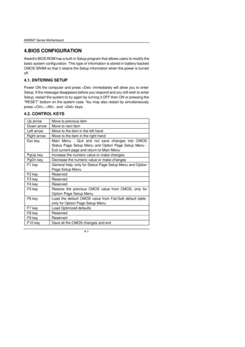
Transcription
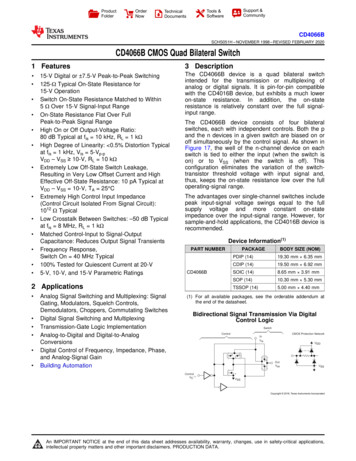
ProductFolderOrderNowSupport &CommunityTools &SoftwareTechnicalDocumentsCD4066BSCHS051H – NOVEMBER 1998 – REVISED FEBRUARY 2020CD4066B CMOS Quad Bilateral Switch1 Features3 Description The CD4066B device is a quad bilateral switchintended for the transmission or multiplexing ofanalog or digital signals. It is pin-for-pin compatiblewith the CD4016B device, but exhibits a much loweron-state resistance. In addition, the on-stateresistance is relatively constant over the full signalinput range.1 15-V Digital or 7.5-V Peak-to-Peak Switching125-Ω Typical On-State Resistance for15-V OperationSwitch On-State Resistance Matched to Within5 Ω Over 15-V Signal-Input RangeOn-State Resistance Flat Over FullPeak-to-Peak Signal RangeHigh On or Off Output-Voltage Ratio:80 dB Typical at fis 10 kHz, RL 1 kΩHigh Degree of Linearity: 0.5% Distortion Typicalat fis 1 kHz, Vis 5-Vp-pVDD – VSS 10-V, RL 10 kΩExtremely Low Off-State Switch Leakage,Resulting in Very Low Offset Current and HighEffective Off-State Resistance: 10 pA Typical atVDD – VSS 10-V, TA 25 CExtremely High Control Input Impedance(Control Circuit Isolated From Signal Circuit):1012 Ω TypicalLow Crosstalk Between Switches: –50 dB Typicalat fis 8 MHz, RL 1 kΩMatched Control-Input to Signal-OutputCapacitance: Reduces Output Signal TransientsFrequency Response,Switch On 40 MHz Typical100% Tested for Quiescent Current at 20-V5-V, 10-V, and 15-V Parametric RatingsThe CD4066B device consists of four bilateralswitches, each with independent controls. Both the pand the n devices in a given switch are biased on oroff simultaneously by the control signal. As shown inFigure 17, the well of the n-channel device on eachswitch is tied to either the input (when the switch ison) or to VSS (when the switch is off). Thisconfiguration eliminates the variation of the switchtransistor threshold voltage with input signal and,thus, keeps the on-state resistance low over the fulloperating-signal range.The advantages over single-channel switches includepeak input-signal voltage swings equal to the fullsupply voltage and more constant on-stateimpedance over the input-signal range. However, forsample-and-hold applications, the CD4016B device isrecommended.Device Information(1)PART NUMBERPACKAGECD4066B2 Applications Analog Signal Switching and Multiplexing: SignalGating, Modulators, Squelch Controls,Demodulators, Choppers, Commutating SwitchesDigital Signal Switching and MultiplexingTransmission-Gate Logic ImplementationAnalog-to-Digital and Digital-to-AnalogConversionsDigital Control of Frequency, Impedance, Phase,and Analog-Signal GainBuilding AutomationBODY SIZE (NOM)PDIP (14)19.30 mm 6.35 mmCDIP (14)19.50 mm 6.92 mmSOIC (14)8.65 mm 3.91 mmSOP (14)10.30 mm 5.30 mmTSSOP (14)5.00 mm 4.40 mm(1) For all available packages, see the orderable addendum atthe end of the datasheet.Bidirectional Signal Transmission Via DigitalControl LogicSwitchControlCMOS Protection NetworkInVispVDDnpnControlVC (1)OutVosVSSnVSSCopyright 2016, Texas Instruments Incorporated1An IMPORTANT NOTICE at the end of this data sheet addresses availability, warranty, changes, use in safety-critical applications,intellectual property matters and other important disclaimers. PRODUCTION DATA.
CD4066BSCHS051H – NOVEMBER 1998 – REVISED FEBRUARY 2020www.ti.comTable of Contents12345678Features .Applications .Description .Revision History.Pin Configuration and Functions Absolute Maximum Ratings .ESD Ratings.Recommended Operating Conditions.Thermal Information .Electrical Characteristics.Switching Characteristics .Typical Characteristics .Parameter Measurement Information . 10Detailed Description . 148.1 Overview . 148.2 Functional Block Diagram . 148.3 Feature Description. 148.4 Device Functional Modes. 149Application and Implementation . 159.1 Application Information. 159.2 Typical Application . 1510 Power Supply Recommendations . 1711 Layout. 1711.1 Layout Guidelines . 1711.2 Layout Example . 1712 Device and Documentation Support . 1812.112.212.312.412.5Receiving Notification of Documentation UpdatesCommunity Resources.Trademarks .Electrostatic Discharge Caution .Glossary .181818181813 Mechanical, Packaging, and OrderableInformation . 184 Revision HistoryNOTE: Page numbers for previous revisions may differ from page numbers in the current version.Changes from Revision G (June 2017) to Revision H Added Junction Temperature details to the Absolute Maximum Ratings table. 4Changes from Revision F (March 2017) to Revision G PagePageChanged From: VSS To: Hi-Z in the SIG OUT/IN column of . 14Changes from Revision E (September 2016) to Revision FPage Corrected the ron VDD 10 V values in the Electrical Characteristics table. . 7 Corrected the y axis scale in Figure 6 . 9Changes from Revision D (September 2003) to Revision EPage Added ESD Ratings table, Feature Description section, Device Functional Modes, Application and Implementationsection, Power Supply Recommendations section, Layout section, Device and Documentation Support section, andMechanical, Packaging, and Orderable Information section . 1 Deleted Ordering Information table, see POA at the end of the data sheet. 1 Changed values in the Thermal Information table to align with JEDEC standards . 42Submit Documentation FeedbackCopyright 1998–2020, Texas Instruments IncorporatedProduct Folder Links: CD4066B
CD4066Bwww.ti.comSCHS051H – NOVEMBER 1998 – REVISED FEBRUARY 20205 Pin Configuration and FunctionsN, J, D, NS, or PW Packages14-Pin PDIP, CDIP, SOIC, SO, or TSSOPTop ViewSIG A IN/OUTSIG A OUT/INSIG B OUT/INSIG B IN/OUTCONTROL BCONTROL CVSS1142133124115106978VDDCONTROL ACONTROL DSIG D IN/OUTSIG D OUT/INSIG C OUT/INSIG C IN/OUTPin FunctionsPINNO.NAMEI/ODESCRIPTION1SIG A IN/OUTI/OInput/Output for Switch A2SIG A OUT/INI/OOutput/Input for Switch A3SIG B OUT/INI/OOutput/Input for Switch B4SIG B IN/OUTI/OInput/Output for Switch B5CONTROL BIControl pin for Switch B6CONTROL CIControl pin for Switch C7VSS—Low Voltage Power Pin8SIG C IN/OUTI/OInput/Output for Switch C9SIG C OUT/INI/OOutput/Input for Switch C10SIG D OUT/INI/OOutput/Input for Switch D11SIG D IN/OUTI/OInput/Output for Switch D12CONTROL DIControl Pin for D13CONTROL AIControl Pin for A14VDD—Power PinSubmit Documentation FeedbackCopyright 1998–2020, Texas Instruments IncorporatedProduct Folder Links: CD4066B3
CD4066BSCHS051H – NOVEMBER 1998 – REVISED FEBRUARY 2020www.ti.com6 Specifications6.1 Absolute Maximum RatingsOver operating free-air temperature range (unless otherwise noted) (1)MINMAXUNITVDDDC supply-voltageVoltages referenced to VSS pin–0.520VVisInput voltageAll inputs–0.5VDD 0.5VIINDC input currentAny one input 10mATJMAX1Maximum junction temperature, ceramic package175 CTJMAX2Maximum junction temperature, plastic package150 CTstgStorage temperature150 C(1)–65Stresses beyond those listed under Absolute Maximum Ratings may cause permanent damage to the device. These are stress ratingsonly, and functional operation of the device at these or any other conditions beyond those indicated under Recommended OperatingConditions is not implied. Exposure to absolute-maximum-rated conditions for extended periods may affect device reliability.6.2 ESD RatingsVALUEV(ESD)(1)(2)Electrostatic dischargeHuman body model (HBM), per ANSI/ESDA/JEDEC JS-001, allpins (1) 500Charged device model (CDM), per JEDEC specification JESD22C101, all pins (2) 1500UNITVJEDEC document JEP155 states that 500-V HBM allows safe manufacturing with a standard ESD control process.JEDEC document JEP157 states that 250-V CDM allows safe manufacturing with a standard ESD control process.6.3 Recommended Operating ConditionsOver operating free-air temperature range (unless otherwise noted)VDDSupply voltageTAOperating free-air temperatureMINMAX318UNITV–55125 C6.4 Thermal InformationCD4066BTHERMAL METRIC (1)N(PDIP)D(SOIC)NS(SO)PW(TSSOP)14 PINS14 PINS14 PINS14 PINSUNITRθJAJunction-to-ambient thermal resistance53.789.588.2119.5 C/WRθJC(top)Junction-to-case (top) thermal resistance41.049.746.148.2 C/WRθJBJunction-to-board thermal resistance33.643.847.061.2 C/WψJTJunction-to-top characterization parameter25.817.416.35.5 C/WψJBJunction-to-board characterization parameter33.543.546.660.6 C/W(1)4For more information about traditional and new thermal metrics, see the Semiconductor and IC Package Thermal Metrics applicationreport.Submit Documentation FeedbackCopyright 1998–2020, Texas Instruments IncorporatedProduct Folder Links: CD4066B
CD4066Bwww.ti.comSCHS051H – NOVEMBER 1998 – REVISED FEBRUARY 20206.5 Electrical CharacteristicsOver operating free-air temperature range (unless otherwise noted)PARAMETERTEST CONDITIONSMINTYP MAX UNITVDD 5 VVis 0 V0.4VDD 5 VVis 5 VVosSwitch output voltage4.6VVDD 10 VVis 0 V0.5VDD 10 VVis 10 V9.5VVVDD 15 VVis 0 V1.5VDD 15 VVis 15 VV13.5VVVDD 5 V15VDD 10 V10VDD 15 V5On-state resistancedifference between anytwo switchesRL 10 kΩ, VC VDDTotal harmonic distortionVC VDD 5 V, VSS –5 V,Vis(p-p) 5 V (sine wave centered on 0 V),RL 10 kΩ, fis 1-kHz sine wave0.4%–3-dB cutoff frequency(switch on)VC VDD 5 V, VSS –5 V, Vis(p-p) 5 V(sine wave centered on 0 V), RL 1 kΩ40MHz–50-dB feedthroughfrequency (switch off)VC VSS –5 V, Vis(p-p) 5 V(sine wave centered on 0 V), RL 1 kΩ1MHz–50-dB crosstalkfrequencyVC(A) VDD 5 V,VC(B) VSS –5 V,Vis(A) 5 Vp-p, 50-Ω source,RL 1 kΩ8MHzCisInput capacitanceVDD 5 V, VC VSS –5 V8pFCosOutput capacitanceVDD 5 V, VC VSS –5 V8pFCiosFeedthroughVDD 5 V, VC VSS –5 V0.5pFΔronTHDVDD 5 VVIHCControl input, high voltage See Figure 7Crosstalk(control input to signaloutput)VC 10 V (square wave),tr, tf 20 ns, RL 10 kΩVDD 10 VTurnon and turnoffpropagation delayVIN VDD, tr, tf 20 ns,CL 50 pF, RL 1 kΩMaximum control inputrepetition rateCIΩ3.5VDD 10 V7VDD 15 V11V50mVVDD 5 V3570VDD 10 V2040VDD 15 V1530Vis VDD, VSS GND,VDD 5 VRL 1 kΩ to GND,VDD 10 VCL 50 pF,VC 10 V (square wavecentered on 5 V), tr, tf 20 ns, VDD 15 VVos 1/2 Vos at 1 kHz6Input capacitance9MHz9.557.5Submit Documentation FeedbackCopyright 1998–2020, Texas Instruments IncorporatedProduct Folder Links: CD4066BnspF5
CD4066BSCHS051H – NOVEMBER 1998 – REVISED FEBRUARY 2020www.ti.comElectrical Characteristics (continued)Over operating free-air temperature range (unless otherwise noted)PARAMETERTEST CONDITIONSMINTYP MAX UNITTA –55 C0.64TA –40 CVDD 5 VVis 0 VVDD 5 VVis 5 VTA 25 C0.610.51TA 85 C0.42TA 125 C0.36TA –55 C–0.64TA –40 C–0.61TA 25 C–0.51Iis–0.42TA 125 C–0.36TA –55 C1.6TA 25 C1.51.3TA 85 CSwitch input currentVDD 10 VVis 10 V1.10.9TA –55 C–1.6TA –40 C–1.5TA 25 C–1.36mATA 85 C–1.1TA 125 C–0.9TA –55 C4.2TA 25 C43.4TA 85 CVDD 15 VVis 15 VmATA 125 CTA –40 CVDD 15 VVis 0 VmATA 85 CTA –40 CVDD 10 VVis 0 VmAmA2.8TA 125 C2.4TA –55 C–4.2TA –40 C–4TA 25 C–3.4mATA 85 C–2.8TA 125 C–2.4Submit Documentation FeedbackCopyright 1998–2020, Texas Instruments IncorporatedProduct Folder Links: CD4066B
CD4066Bwww.ti.comSCHS051H – NOVEMBER 1998 – REVISED FEBRUARY 2020Electrical Characteristics (continued)Over operating free-air temperature range (unless otherwise noted)PARAMETERTEST CONDITIONSMINTYP MAX UNITTA –55 C0.25TA –40 CVIN 0 to 5 VVDD 5 VVIN 0 to 10 VVDD 10 VIDD0.25TA 25 CQuiescent device current0.01TA 85 C7.5TA 125 C7.5TA –55 C0.5TA –40 C0.5TA 25 C0.01VIN 0 to 20 VVDD 20 V15TA 125 C15TA –55 C10.0130TA 125 C30TA –55 C5TA –40 C5TA 25 C0.025TA 85 C150TA 125 C150VDD 10 V470 1050TA 85 C1200TA 125 C1300TA –55 C310TA –40 C330TA 25 C180400TA 85 C500TA 125 C500TA –55 C200TA 25 CProduct Folder Links: CD4066BµAΩ210125240TA 85 C300TA 125 C320Submit Documentation FeedbackCopyright 1998–2020, Texas Instruments IncorporatedµA850TA 25 CTA –40 CVDD 15 VµA800TA –40 Cron1TA 85 CVDD 5 VµA1TA 25 CTA –55 CV - V SS )to ( DDOn-state resistance (max) VC VDD,2RL 10 kΩ returned Vis VSSto VDD0.5TA 85 CTA –40 CVIN 0 to 15 VVDD 15 V0.257
CD4066BSCHS051H – NOVEMBER 1998 – REVISED FEBRUARY 2020www.ti.comElectrical Characteristics (continued)Over operating free-air temperature range (unless otherwise noted)PARAMETERTEST CONDITIONSVDD 5 V Iis 10 µA,Vis VSS, VOS VDD, andVis VDD, VOS VSSControl input,low voltage (max)VILCVDD 10 VVDD 15 VMINTYP MAX UNITTA –55 C1TA –40 C1TA 25 C1TA 85 C1TA 125 C1TA –55 C2TA –40 C2TA 25 C2TA 85 C2TA 125 C2TA –55 C2TA –40 C2TA 25 C2TA 85 C2TA 125 C2TA –55 CIINInput current (max)Vis VDD, VDD – VSS 18 V,VCC VDD – VSSVDD 18 VV 0.1TA –40 C 0.1–5TA 25 C 10 0.1TA 85 C 1TA 125 C 1µA6.6 Switching CharacteristicsTA 25 CPARAMETERtpdtplhtphl8FROMSignal inputSignal inputSignal inputTOSignal outputSignal outputSignal outputTEST CONDITIONSVIN VDD, tr, tf 20 ns,CL 50 pF, RL 1 kΩVIN VDD, tr, tf 20 ns,CL 50 pF, RL 1 kΩVIN VDD, tr, tf 20 ns,CL 50 pF, RL 1 kΩSubmit Documentation FeedbackVCCMINTYP MAX5V204010 V102015 V7155V357010 V204015 V15305V357010 V204015 V1530UNITnsnsnsCopyright 1998–2020, Texas Instruments IncorporatedProduct Folder Links: CD4066B
CD4066Bwww.ti.comSCHS051H – NOVEMBER 1998 – REVISED FEBRUARY 2020600Supply Voltage (VDD VSS) 5 V500TA 125 Cr Channel On-State Resistance Ωonr Channel On-State Resistance Ωon6.7 Typical Characteristics400300 25 C200 55 C1000 4 3 2 101234300Supply Voltage (VDD VSS) 10 V250TA 125 C200 25 C150 55 C100500 10 7.5 5Vis Input Signal Voltage V 2.502.557.592CS-27326RISupply Voltage (VDD VSS) 15 V300250200TA 125 C150 25 C100 55 C500 7.5 5 2.502.557.592CS-27327RIFigure 2. Typical ON-State Resistance vs Input SignalVoltage (All Types)r Channel On-State Resistance Ωonr Channel On-State Resistance ΩonFigure 1. Typical ON-State Resistance vs Input SignalVoltage (All Types) 1010TA 125 C600Supply Voltage (VDD VSS) 5 V50040030020010 V 15 V1000 10 7.5 5 2.502.557.592CS-27329RIFigure 3. Typical ON-State Resistance vs Input SignalVoltage (All Types)92CS-27330RIFigure 4. Typical ON-State Resistance vs Input SignalVoltage (All Types)104VO Output Voltage V210VC VDDVDDCD4066B1 of 4SwitchesVosRLVSS 2All unused terminals areconnected to VSS 3 3 2 101234PD Power Dissipation Per Package µ W63Vis10Vis Input Signal Voltage VVis Input Signal Voltage V 110Vis Input Signal Voltage VTA 25 C42Supply Voltage(VDD) 15 V1038610 f Switching Frequency kHzVI Input Voltage V92CS-30919Figure 5. Typical ON Characteristics for 1 of 4 ChannelsFigure 6. Power Dissipation per Package vs SwitchingFrequencySubmit Documentation FeedbackCopyright 1998–2020, Texas Instruments IncorporatedProduct Folder Links: CD4066B9
CD4066BSCHS051H – NOVEMBER 1998 – REVISED FEBRUARY 2020www.ti.com7 Parameter Measurement InformationI isV isCD4066B1 of 4 Switchesr on V os V is í V os I is Copyright 2016, Texas Instruments IncorporatedFigure 7. Determination of ron as a Test Condition for Control-Input High-Voltage (VIHC) SpecificationKeithley160 DigitalMultimeterVDDTGOn10 kΩ1-kΩRangeYX-YPlotterVSSH. P.Moseley7030AX92CS-22716Figure 8. Channel On-State Resistance Measurement CircuitCiosVC 5 VVDD 5 VCD4066B1 of 4SwitchesCisVSS 5 VCos92CS-30921Measured on Boonton capacitance bridge, model 75a (1 MHz);test-fixture capacitance nulled out.Figure 9. Typical On Characteristics for One of Four Channels10Submit Documentation FeedbackCopyright 1998–2020, Texas Instruments IncorporatedProduct Folder Links: CD4066B
CD4066Bwww.ti.comSCHS051H – NOVEMBER 1998 – REVISED FEBRUARY 2020Parameter Measurement Information (continued)VDDVC VSSCD4066B1 of 4SwitchesVis VDDVosIVSS92CS-30922All unused terminals are connected to VSS.Figure 10. Off-Switch Input or Output LeakageVDDVC VDDCD4066B1 of 4SwitchesVisVSSVos200 kΩ50 pFVDDtr tf 20 ns92CS-30923All unused terminals are connected to VSS.Figure 11. Propagation Delay Time Signal Input(Vis) to Signal Output (Vos) 10 VVDDVCVistr tf 20 ns1 kΩCD4066B1 of 4SwitchesVos10 kΩVSS92CS-30924All unused terminals are connected to VSS.Figure 12. Crosstalk-Control Input to Signal OutputSubmit Documentation FeedbackCopyright 1998–2020, Texas Instruments IncorporatedProduct Folder Links: CD4066B11
CD4066BSCHS051H – NOVEMBER 1998 – REVISED FEBRUARY 2020www.ti.comParameter Measurement Information (continued)VDDVDDVC VDDt r t f 20 nsVDDVosCD4066B1 of 4Switches1 kŸ50 pFVSSCopyright 2016, Texas Instruments IncorporatedAll unused pins are connected to VSS.Delay is measured at Vos level of 10% from ground (turn-on) or on-state output level (turn-off).Figure 13. Propagation Delay, tPLH, tPHL Control-Signal OutputtrVC10%tf10 V90%50%0VRepetitionRatetr t f 20 nsVVosV OS at1kHzOS2VDD 10 VVCVis 10 VCD4066B1 of 4SwitchesVOS50 pFVOSat1kHz21 kŸVSSCopyright 2016, Texas Instruments IncorporatedAll unused pins are connected to VSS.Figure 14. Maximum Allowable Control-Input Repetition Rate12Submit Documentation FeedbackCopyright 1998–2020, Texas Instruments IncorporatedProduct Folder Links: CD4066B
CD4066Bwww.ti.comSCHS051H – NOVEMBER 1998 – REVISED FEBRUARY 2020Parameter Measurement Information (continued)VDDInputsVDDIVSS92CS-27555VSSMeasure inputs sequentially to both VDD and VSS. Connect all unused inputs to either VDD or VSS. Measure control inputs only.Figure 15. Input Leakage-Current Test Circuit10ClockReset14239PE J 1 J 2 J3 J 41517ClockJ5ExternalReset13CD4018B314PE J1J215141/4 CD4066B912J3 J4J57CD4018BQ1 Q21Q1 Q252101245237221/3 CD4049B56489864CD4001B1091165121365 111113Channel 3Channel 44CD4066B8911101533441/4 CD4066BLPFSignalOutputsChannel 110 NŸ1/6 CD4049B212121112Channel 234101012Channel 11269SignalInputs51/3 CD4049B5CD4001B31213138Channel 210 NŸCD4066B11LPF9LPFChannel 310 kŸ10 NŸ10LPFChannel 410 NŸCopyright 2016, Texas Instruments IncorporatedFigure 16. Four-Channel PAM Multiplex System DiagramSubmit Documentation FeedbackCopyright 1998–2020, Texas Instruments IncorporatedProduct Folder Links: CD4066B13
CD4066BSCHS051H – NOVEMBER 1998 – REVISED FEBRUARY 2020www.ti.com8 Detailed Description8.1 OverviewCD4066B has four independent digitally controlled analog switches with a bias voltage of VSS to allow fordifferent voltage levels to be used for low output. Both the p and the n devices in a given switch are biased on oroff simultaneously by the control signal. As shown in Figure 17, the well of the n-channel device on each switchis tied to either the input (when the switch is on) or to VSS (when the switch is off). Thus, when the control of thedevice is low, the output of the switch goes to VSS and when the control is high the output of the device goes toVDD.8.2 Functional Block DiagramSwitchControlCMOS Protection NetworkInVispVDDnpOutVosnVSSnControlVC (1)VSSCopyright 2016, Texas Instruments Incorporated(1)All control inputs are protected by the CMOS protection network.(2)All p substrates are connected to VDD.(3)Normal operation control-line biasing: switch on (logic 1), VC VDD; switch off (logic 0), VC VSS.(4)Signal-level range: VSS Vis VDD.Figure 17. Schematic Diagram of One-of-Four Identical Switches and Associated Control Circuitry8.3 Feature DescriptionEach switch has different control pins, which allows for more options for the outputs. Bias Voltage allows thedevice to output a voltage other than 0 V when the device control is low. The CD4066B has a large absolutemaximum voltage for VDD of 20 V.8.4 Device Functional ModesAdded Junction Temperature details to the Absolute Maximum Ratings table lists the functions of this device.Table 1. Function TableINPUTS14OUTPUTSIG IN/OUTCONTROLSIG OUT/INHHHLHLXLHi-ZSubmit Documentation FeedbackCopyright 1998–2020, Texas Instruments IncorporatedProduct Folder Links: CD4066B
CD4066Bwww.ti.comSCHS051H – NOVEMBER 1998 – REVISED FEBRUARY 20209 Application and ImplementationNOTEInformation in the following applications sections is not part of the TI componentspecification, and TI does not warrant its accuracy or completeness. TI’s customers areresponsible for determining suitability of components for their purposes. Customers shouldvalidate and test their design implementation to confirm system functionality.9.1 Application InformationIn applications that employ separate power sources to drive VDD and the signal inputs, the VDD current capabilityshould exceed VDD/RL (RL effective external load of the four CD4066B device bilateral switches). This provisionavoids any permanent current flow or clamp action on the VDD supply when power is applied or removed from theCD4066B device.In certain applications, the external load-resistor current can include both VDD and signal-line components. Toavoid drawing VDD current when switch current flows into pins 1, 4, 8, or 11, the voltage drop across thebidirectional switch must not exceed 0.8 V (calculated from ron values shown).No VDD current flows through RL if the switch current flows into pins 2, 3, 9, or 10.9.2 Typical Application5V0 5 VAnalog Inputs ( 5 V)VDD 5 VVDD 5 tsVSS 0 VVEE 5 VAnalog Outputs ( 5 V)VSS 5 V92CS-30927Figure 18. Bidirectional Signal Transmission Through Digital Control Logic9.2.1 Design RequirementsThis device uses CMOS technology and has balanced output drive. Avoid bus contention because it can drivecurrents in excess of maximum limits. The high drive also creates fast edges into light loads, so consider routingand load conditions to prevent ringing.9.2.2 Detailed Design Procedure1. Recommended Input Conditions:– For rise time and fall time specifications, see Δt/Δv in Recommended Operating Conditions.– For specified high and low levels, see VIH and VIL in Recommended Operating Conditions.2. Recommended Output Conditions:– Load currents should not exceed 10 mA.Submit Documentation FeedbackCopyright 1998–2020, Texas Instruments IncorporatedProduct Folder Links: CD4066B15
CD4066BSCHS051H – NOVEMBER 1998 – REVISED FEBRUARY 2020www.ti.comTypical Application (continued)9.2.3 Application Curve104PD Power Dissipation Per Package µ W6TA 25 C42Supply Voltage(VDD) 15 V1038610 f Switching Frequency kHzFigure 19. Power Dissipation vs. Switching Frequency16Submit Documentation FeedbackCopyright 1998–2020, Texas Instruments IncorporatedProduct Folder Links: CD4066B
CD4066Bwww.ti.comSCHS051H – NOVEMBER 1998 – REVISED FEBRUARY 202010 Power Supply RecommendationsThe power supply can be any voltage between the MIN and MAX supply voltage rating located in RecommendedOperating Conditions.Each VCC pin should have a good bypass capacitor to prevent power disturbance. For devices with a singlesupply, 0.1-µF is recommended; if there are multiple VCC pins, then 0.01-µF or 0.022-µF is recommended foreach power pin. It is acceptable to parallel multiple bypass capacitors to reject different frequencies of noise. A0.1-µF and a 1-µF are commonly used in parallel. The bypass capacitor should be installed as close to the powerpin as possible for best results.11 Layout11.1 Layout GuidelinesWhen using multiple bit logic devices inputs must never float.In many cases, functions or parts of functions of digital logic devices are unused, for example, when only twoinputs of a triple-input and gate are used or only 3 of the 4 buffer gates are used. Such input pins must not be leftunconnected because the undefined voltages at the outside connections result in undefined operational states.All unused inputs of digital logic devices must be connected to a high or low bias to prevent them from floating.The logic level that should be applied to any particular unused input depends on the function of the device.Generally they are tied to GND or VCC, whichever makes more sense or is more convenient. It is generallyacceptable to float outputs, unless the part is a transceiver. If the transceiver has an output enable pin, it disablesthe output section of the part when asserted. This does not disable the input section of the I/Os, so they cannotfloat when disabled.11.2 Layout ExampleVccInputUnused InputOutputUnused InputOutputInputFigure 20. Diagram for Unused InputsSubmit Documentation FeedbackCopyright 1998–2020, Texas Instruments IncorporatedProduct Folder Links: CD4066B17
CD4066BSCHS051H – NOVEMBER 1998 – REVISED FEBRUARY 2020www.ti.com12 Device and Documentation Support12.1 Receiving Notification of Documentation UpdatesTo receive notification of documentation updates, navigate to the device product folder on ti.com. In the upperright corner, click on Alert me to register and receive a weekly digest of any product information that haschanged. For change details, review the revision history included in any revised document.12.2 Community ResourcesTI E2E support forums are an engineer's go-to source for fast, verified answers and design help — straightfrom the experts. Search existing answers or ask your own question to get the quick design help you need.Linked content is provided "AS IS" by the respective contributors. They do not constitute TI specifications and donot necessarily reflect TI's views; see TI's Terms of Use.12.3 TrademarksE2E is a trademark of Texas Instruments.All other trademarks are the property of their respective owners.12.4 Electrostatic Discharge CautionThis integrated circuit can be damaged by ESD. Texas Instruments recommends that all integrated circuits be handled withappropriate precautions. Failure to observe proper handling and installation procedures can cause damage.ESD damage can range from subtle performance degradation to complete device failure. Precision integrated circuits may be moresusceptible to damage because very small parametric changes could cause the device not to meet its published specifications.12.5 GlossarySLYZ022 — TI Glossary.This glossary lists and explains terms, acronyms, and definitions.13 Mechanical, Packaging, and Orderable InformationThe following pages include mechanical, packaging, and orderable information. This information is the mostcurrent data available for the designated devices. This data is subject to change without notice and revision ofthis document. For browser-based versions of this data sheet, refer to the left-hand navigation.18Submit Documentation FeedbackCopyright 1998–2020, Texas Instruments IncorporatedProduct Folder Links: CD4066B
PACKAGE OPTION ADDENDUMwww.ti.com10-Sep-2021PACKAGING INFORMATIONOrderable DeviceStatus(1)Package Type Package Pins PackageDrawingQtyEco Plan(2)Lead finish/Ball materialMSL Peak TempOp Temp ( C)Device Marking(3)(4/5)(6)CD4066BEACTIVEPDIPN1425RoHS & GreenNIPDAU SNN / A for Pkg Type-55 to 125CD4066BECD4066BEE4ACTIVEPDIPN1425RoHS &Non-GreenNIPDAUN / A for Pkg Type-55 to 125CD4066BECD4066BFACTIVECDIPJ141Non-RoHS& GreenSNPBN / A for Pkg Type-55 to 125CD4066BFCD4066BF3AACTIVECDIPJ141Non-RoHS& GreenSNPBN / A for Pkg Type-55 to 125CD4066BF3ACD4066BMACTIVESOICD1450RoHS & GreenNIPDAULevel-1-260C-UNLIM-55 to 125CD4066BMCD4066BM96ACTIVESOICD142500RoHS & GreenNIPDAU SNLevel-1-260C-UNLIM-55 to 125CD4066BMCD4066BM96E4ACTIVESOICD142500RoHS & GreenNIPDAULevel-1-260C-UNLIM-55 to 125CD4066BMCD4066BM96G4ACTIVESOICD142500RoHS & GreenNIPDAULevel-1-260C-UNLIM-55 to 125CD4066BMCD4066BMTACTIVESOICD14250RoHS & GreenNIPDAULevel-1-260C-UNLIM-55 to 125CD4066BMCD4066BNSACTIVESONS1450RoHS & 42000RoHS & GreenNIPDAULevel-1-260C-UNLIM-55 to 125CD4066BCD4066BPWACTIVETSSOPPW1490RoHS & GreenNIPDAULevel-1-260C-UNLIM-55 to 125CM066BCD4066BPWG4ACTIVETSSOPPW1490RoHS & GreenNIPDAULevel-1-260C-UNLIM-55 to 125CM066BCD4066BPWRACTIVETSSOPPW142000RoHS & GreenNIPDAU SNLevel-1-260C-UNLIM-55
switch is tied to either the input (when the switch is on) or to VSS (when the switch is off). This configuration eliminates the variation of the switch-transistor threshold voltage with input signal and, thus, keeps the on-s