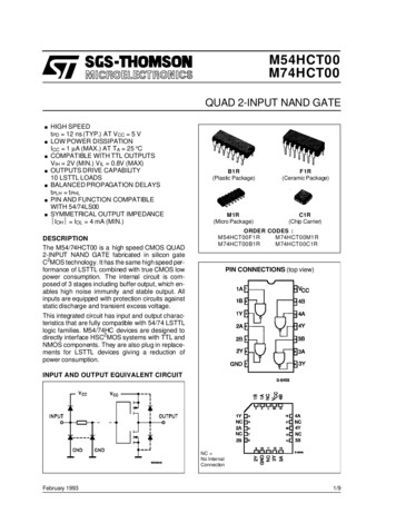
Transcription
M54HCT00M74HCT00QUAD 2-INPUT NAND GATE.HIGH SPEEDtPD 12 ns (TYP.) AT VCC 5 VLOW POWER DISSIPATIONICC 1 µA (MAX.) AT TA 25 CCOMPATIBLE WITH TTL OUTPUTSVIH 2V (MIN.) VIL 0.8V (MAX)OUTPUTS DRIVE CAPABILITY10 LSTTL LOADSBALANCED PROPAGATION DELAYStPLH tPHLPIN AND FUNCTION COMPATIBLEWITH 54/74LS00SYMMETRICAL OUTPUT IMPEDANCE IOH IOL 4 mA (MIN.)DESCRIPTIONThe M54/74HCT00 is a high speed CMOS QUAD2-INPUT NAND GATE fabricated in silicon gateC2MOS technology. It has the same high speed performance of LSTTL combined with true CMOS lowpower consumption. The internal circuit is composed of 3 stages including buffer output, which enables high noise immunity and stable output. Allinputs are equipped with protection circuits againststatic discharge and transient excess voltage.B1R(Plastic Package)F1R(Ceramic Package)M1R(Micro Package)C1R(Chip Carrier)ORDER CODES :M54HCT00F1RM74HCT00M1RM74HCT00B1RM74HCT00C1RPIN CONNECTIONS (top view)This integrated circuit has input and output characteristics that are fully compatible with 54/74 LSTTLlogic families. M54/74HC devices are designed todirectly interface HSC2MOS systems with TTL andNMOS components. They are also plug in replacements for LSTTL devices giving a reduction ofpower consumption.INPUT AND OUTPUT EQUIVALENT CIRCUITNC No InternalConnectionFebruary 19931/9
M54/M74HCT00TRUTH TABLEIEC LOGIC SYMBOLABYLLLHHHHLHHHLPIN DESCRIPTIONPIN No1, 4, 9, 12SYMBOL1A to 4ANAME AND FUNCTIONData Inputs2, 5, 10, 131B to 4BData Inputs3, 6, 8, 1171Y to 4YGNDData OutputsGround (0V)14VCCPositive Supply VoltageLOGIC DIAGRAMABSOLUTE MAXIMUM RATINGSSymbolICCValueUnitVCCVISupply VoltageDC Input VoltageParameter-0.5 to 7-0.5 to VCC 0.5VVVODC Output Voltage-0.5 to VCC 0.5VIIKDC Input Diode Current 20mAIOKDC Output Diode Current 20mAIOor IGNDDC Output Source Sink Current Per Output PinDC VCC or Ground Current 25 50mAmAPDPower Dissipation500 (*)mWTstgTLStorage TemperatureLead Temperature (10 sec)-65 to 150300ooCCAbsolute Maximum Ratings are those values beyond which damage to the device may occur. Functional operation under these condition isnotimplied.(*) 500 mW: 65 oC derate to 300 mW by 10mW/oC: 65 oC to 85 oC2/9
M54/M74HCT00RECOMMENDED OPERATING CONDITIONSSymbolParameterValueUnitVVVCCVISupply VoltageInput Voltage4.5 to 5.50 to VCCVOOutput Voltage0 to VCCToptr, tfOperating Temperature: M54HC SeriesM74HC SeriesInput Rise and Fall Time (VCC 4.5 to 5.5V)Vo-55 to 125-40 to 850 to 500CCnsoDC SPECIFICATIONSTest ConditionsSymbolParameterVIHHigh Level InputVoltageV ILLow Level InputVoltageV OHHigh LevelOutput VoltageVOLIIICC ICCLow Level OutputVoltageInput LeakageCurrentQuiescent SupplyCurrentAdditional worstcase supplycurrentValueTA 25 oC54HC and 74HCVCC(V)Min.2.04.5to5.54.5to5.5Typ.Max.-40 to 85 oC -55 to 125 oC74HC54HCMin.2.00.84.5VI IO -20 µAVIHor IO -4.0 mAV IL4.5VI IO 20 µAVIHor IO 4.0 mAV 10UnitVV0.00.10.10.10.170.260.330.40VI VCC or GND 0.1 1 1µA5.5VI VCC or GND11020µA5.5Per Input pinVI 0.5V orV I 2.4VOther Inputs atV CC or GNDIO 02.02.93.0mA5.5V3/9
M54/M74HCT00AC ELECTRICAL CHARACTERISTICS (C L 50 pF, Input t r tf 6 ns)Test ConditionsValueo-40 to 85 oC -55 to 125 oC74HC54HCMin. Max. Min. Max.SymbolParameterVCC(V)TA 25 C54HC and 74HCMin. Typ. Max.tTLHtTHLOutput TransitionTime4.58151922nstPLHtPHLPropagationDelay Time4.512192429ns540101010pFpFCINCPD (*)Input CapacitancePower DissipationCapacitanceUnit(*) CPD is defined as the value of the IC’s internal equivalent capacitance which is calculated from the operating current consumption without load.(Refer to Test Circuit). Average operting current can be obtained by the following equation. ICC(opr) CPD VCC fIN ICC/4 (per Gate)SWITCHING CHARACTERISTICS TEST CIRCUITTEST CIRCUIT ICC (Opr.)INPUT WAVEFORM IS THE SAME AS THAT IN CASE OF SWITCHING CHARACTERISTICS TEST.4/9
M54/M74HCT00Plastic DIP14 MECHANICAL 1.270.1302.540.0500.100P001A5/9
M54/M74HCT00Ceramic DIP14/1 MECHANICAL 4060.3070.3170.200P053C6/9
M54/M74HCT00SO14 MECHANICAL 190.250.0070.010C0.50.019c145 51.270.0190.050MS0.680.0268 (max.)P013G7/9
M54/M74HCT00PLCC20 MECHANICAL 027A8/9
M54/M74HCT00Information furnished is believed to be accurate and reliable. However, SGS-THOMSON Microelectronics assumes no responsability for theconsequences of use of such information nor for any infringement of patents or other rights of third parties which may results from its use. Nolicense is granted by implication or otherwise under any patent or patent rights of SGS-THOMSON Microelectronics. Specifications mentionedin this publication are subject to change without notice. This publication supersedes and replaces all information previously supplied.SGS-THOMSON Microelectronics products are not authorized for use ascritical components in life support devices or systems without expresswritten approval of SGS-THOMSON Microelectonics. 1994 SGS-THOMSON Microelectronics - All Rights ReservedSGS-THOMSON Microelectronics GROUP OF COMPANIESAustralia - Brazil - France - Germany - Hong Kong - Italy - Japan - Korea - Malaysia - Malta - Morocco - The Netherlands Singapore - Spain - Sweden - Switzerland - Taiwan - Thailand - United Kingdom - U.S.A9/9
WITH 54/74LS00 SYMMETRICAL OUTPUT IMPEDANCE IOH IOL 4 mA (MIN.) The M54/74HCT00 is a high speed CMOS QUAD 2-INPUT NAND GATE fabricated in silicon gate C2MOStechnology.Ithasthesamehighspeedper-formance of LSTTL combined with true CMOS low power consumption. The internal circuit is com- posedof 3 stagesincluding bufferoutput, which en-ables high