Transcription
A Synthesis Methodology for Application-SpecificLogic-in-Memory DesignsH. Ekin Sumbul, Kaushik Vaidyanathan, Qiuling Zhu, Franz Franchetti, Larry PileggiElectrical & Computer Engineering Department, Carnegie Mellon University5000 Forbes Avenue, Pittsburgh, PA 15213 USA{hsumbul, kvaidya1, qiulingz, franzf, pileggi}@andrew.cmu.eduABSTRACTFor deeply scaled digital integrated systems, the power requiredfor transporting data between memory and logic can exceed thepower needed for computation, thereby limiting the efficacy ofsynthesizing logic and compiling memory independently.Logic-in-Memory (LiM) architectures address this challenge byembedding logic within the memory block to perform basicoperations on data locally for specific functions. While customsmart memories have been successfully constructed for variousapplications, a fully automated LiM synthesis flow enablesarchitectural exploration that has heretofore not been possible. Inthis paper we present a tool and design methodology for LiMphysical synthesis that performs co-design of algorithms andarchitectures to explore system level trade-offs. The resultinglayouts and timing models can be incorporated within anyphysical synthesis tool. Silicon results shown in this paperdemonstrate a 250x performance improvement and 310x energysavings for a data-intensive application example.Categories and Subject DescriptorsB.7.1 [IC]: Types and Design Styles - memory technologiesGeneral TermsDesign, PerformanceKeywordsApplication specific synthesis, embedded logic-in-memory, smartmemory, SRAM, SpGEMM.1. INTRODUCTIONEmbedded memory occupies more than 50% of the overallchip area in a modern SoC (System on Chip) design [5]. Largecompiled memory blocks with mostly-square aspect ratios are themost area efficient choice to minimize the periphery andlithographic area penalties, however, for data-intensiveapplications, most of the performance and energy is spent ontransferring on-chip data over long distances. One solution toaddress this problem is to co-optimize the algorithm, architecture,and hardware, wherein finely tailored small memory arrays,integrated with application-level knowledge, are used to localizethe computation and minimize the data transport over longdistances. Such application-specific targeting, however, generallyincurs a high cost of custom design. Alternatively, compilingsmall granular arrays of embedded memory blocks following aPermission to make digital or hard copies of all or part of this work for personal orclassroom use is granted without fee provided that copies are not made ordistributed for profit or commercial advantage and that copies bear this notice andthe full citation on the first page. Copyrights for components of this work ownedby others than ACM must be honored. Abstracting with credit is permitted. Tocopy otherwise, or republish, to post on servers or to redistribute to lists, requiresprior specific permission and/or a fee. Request permissions fromPermissions@acm.org.DAC '15, June 07 - 11, 2015, San Francisco, CA, USACopyright 2015 ACM 978-1-4503-3520-1/15/06 entional ASIC approach results in area inefficiency. Thissuggests the need for a design methodology that effectivelyaddresses the challenges of memory-intensive applications whilemaintaining an affordable design cost.One enabler for creating such a methodology comes fromscaling trends of sub-20nm technology nodes. Restrictivepatterning in deeply scaled nodes constrains designers to mapmemory and logic to a small set of well-characterized layoutpatterns [8]. Therefore, while memory compilers have beentraditionally used to assemble hard IP layout slices of bitcells andperiphery, restrictive patterning makes the patterning the onlycritical “hard IP.” Moreover, while restrictive patterning isseemingly an impediment for layout efficiency, it does provide anopportunity to place memory cells and random logic gates in closeproximity without creating lithographic hotspots, thereby avoidingarea spacing penalties. Leveraging this technology constraint as a“feature,” the opportunity for synthesis of smart memory blockswas proposed in [6], wherein specialized computation logic andembedded memory could be tightly integrated for localizedcomputation and energy savings. With lithographically compatiblememory and logic cells, any application specific customizationcan be reliably synthesized into the embedded memory block.The energy and performance benefits of localizing computationfor data-intensive applications are well known [2][3][7][11][13].There are various examples of “processor-in-memory” designswherein processing units are placed in memory abstraction [2][3],or more recently, near data computing in 3D and 2.5D stacks toprovide more bandwidth with less energy [11]. It has also beenshown that various data intensive applications highly benefit fromLiM blocks [12][13]. However, there remains the need forphysical synthesis (rather than compilation) of LiM blocks thatare compatible with a full chip physical synthesis and offer theability of system-level exploration.We propose a LiM methodology whereby the memory arraysare physically synthesized from “memory bricks” that representthe lowest level of physical abstraction (analogous to standardcells). The logic cells and memory peripherals are comprised ofstandard logic gates that are lithography-pattern compatible withthe memory bricks. With memory bricks and logic cells at thesame physical abstraction level, the conventional black boxmemory block becomes a “white box” since the boundarybetween memory and logic disappears. This enables memoryarrays to be distributed in a fine-grained manner, thereby reducingsignal travel distances and allowing the inside and outside of anymemory block to be optimized across its boundary forperformance, energy, and area. This automated synthesis furtherenables rapid design-space exploration for the overall system bygenerating pareto-curves of possible block designs.We demonstrate our LiM synthesis methodology for thedata-intensive application of Generalized Sparse Matrix - SparseMatrix Multiplication (SpGEMM). SpGEMM is a core primitivein graph processing applications such as graph contraction or
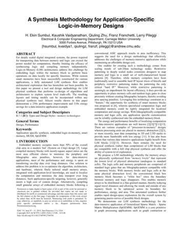
shortest-path algorithms, but traditionally cause very highunpredictable data traffic as the sparse matrices are structurallylarge and unpredictable [4]. We implemented two separate designsas low-power accelerators for SpGEMM algorithm in 65nmCMOS technology. A baseline design is implemented withconventional ASIC flow, and a LiM based design is implementedby using our proposed methodology where design-rule compliantmemory bricks are generated by our automation flow. Bothimplementations use the same bitcells and have comparable areafor a fair comparison. Silicon results show that our LiM basedSpGEMM design provides dramatic benefits up to 250x speed-upand 310x better energy efficiency compared to the baseline design,coming from the co-design of algorithm and hardware.In this paper, background on LiM design is provided in SectionII, and our LiM synthesis flow is described in Section III. SectionIV highlights details on the implemented SpGEMM system, andSection V provides analysis of the LiM based chip results. A finaldiscussion on the overall flow is given in Section VI.2. BACKGROUND2.1 Restrictive patterning enablementFigure 1. Metal-1 SEMS from a 14nm IBM test-chip showingbitcell printability when random logic is put next to bitcellarrays [10].As CMOS scales to sub-22nm technology nodes with 193nmimmersion lithography, design rules become increasingly complexand grow in number [8]. A pattern construct based layout designapproach can provide an efficient and affordable interfacebetween design and manufacturing by limiting the number ofpatterns used to construct a block design [6]. Then logic andmemory bitcells can be constructed from a common set ofpre-characterized layout patterns that are lithography compatible.To demonstrate this patterning influence, Fig. 1 shows threeScanning Electron Microscope (SEM) images for Metal-1 layerscorresponding to 14nm SOI FinFET based bitcells and logicstandard cells as described in [10]. First, bitcell printability in theneighborhood of other bitcells is shown in Fig.1.a. Next, designrule compliant standard cells following conventional layout styleare shown to hurt the printability in Fig.1.b. However, the regularpatterned standard cells next to bitcells do not impact printability,as shown in Fig.1.c. These results validate that restrictivepatterning can enable logic and embedded memory cells that aretightly integrated without requiring extra spacing for lithographycompatibility.2.2 Application-specific smart-memoriesCustomized smart-memories have been proposed andimplemented for a varying set of applications to achieve thelocalized computation that leverages in-memory bandwidth forperformance and saves energy by minimizing wasted data traffic.Data-intensive architecture (DIVA) [2] is a processing-in-memorysystem where multiple smart-memory co-processors are put in atraditional processor to accelerate several instructions by locallyexecuting them within the smart-memory. Computational RAM(CRAM) [3] is another in-memory processing architecturewherein simple computational logic is pitch-matched and placedunder memory columns, such that memory works either as atraditional memory or configured as a single instruction, multipledata (SIMD) smart-memory. Using this technique, parallel work islocalized and in-memory bandwidth is used efficiently for variousapplications such as computer graphics, image processing, etc.Recently with the proliferation of 3D and 2.5D IC stacks andeffective utilization of through silicon vias (TSV), near memorycomputation examples also leverage the high bandwidth thatTSVs provide in between the stacked memories and the core asanother degree of localization. For instance, “smart-3D” [11]architecture demonstrates how to maximize the useful data trafficin between stacked DRAM caches and the processor to minimizeoverall execution time. Alternatively, focusing on low-levelaspects of the embedded memory, an SRAM can be implementedby choosing and tailoring its bitcells carefully for the targetapplication as well.There are also various examples that embed functionality intothe SRAM to perform specific tasks for the application. A parallelaccess memory, for instance, is demonstrated in [7] for powerefficient motion estimation. The parallel access memory stores a2D image pixel array with a size of K x L, and allows randomaccess of pixels in a window of m x n in a single cycle (wherem K and n L). For a traditional ASIC approach, parallel accessmemory is realized by implementing logic blocks next to parallelaccessible SRAM banks. 2D pixels are distributed to m.n parallelmemory banks for a conflict-free access, however, this does notexploit the address pattern commonality between the accessedpixels. Moreover, area and energy penalties are incurred when theimage or access window size is large. For the same functionality,the smart-memory in [7] exploited the address patterncommonality and implemented an application-specific SRAMwith shared and customized decoders. Row decoders are sharedbetween m banks and customized to activate n adjacent wordlineswith respect to single address. A column decoder is added undereach bank group to select a single element per column from theactivated multiple rows. With this customization, the same parallelaccess functionality can be handled inside the memory block withsignificantly less power and area.Based on the same parallel access memory proposed in [7], asmart interpolation memory is proposed in [13] to accelerate thebottleneck of polar to rectangular grid conversion in SyntheticAperture Radar application in an energy efficient way. Theproposed interpolation memory is a LiM based seed table thatuses a parallel access memory as a smaller seed table andinterpolates the required data on the fly as if it is readily stored.Experimental simulation results in [13] show that an applicationspecific LiM based architectures have great potential forimproving the performance for such data-intensive applications.3. LiM SYNTHESIS METHODOLOGYWhile the design in [7] was an expensive manualcustomization, by leveraging the restrictive patterning for deeplyscaled technologies we propose to fully synthesize logic andmemory using the pattern constructs as the only necessary hard IP.By directly synthesizing application-specific functionality into theLiM block design in a fine-grained manner, smart-memorieswould not be custom designed at great cost, or compiled fromhard IP slices at the expense of significant loss of performanceand area. Moreover, with a fully automated synthesis approach,rapid design-space exploration and co-optimization of hardwareand algorithm would be available for system level exploration.
Figure 2. LiM synthesis flow: LiM system is synthesized fromits RTL description. Custom periphery and computation logicare mapped to standard cells, bitcell arrays are mapped to“Memory Bricks”.Overall flow. A high-level overview of our LiM synthesis flow isshown in Fig.2. Custom periphery and logic are mapped tocompatible standard cells, and bitcell arrays are mapped to“memory bricks.” Then using a conventional physical synthesisflow, smart-memory blocks are described in RTL, and physicallysynthesized using the gate-level netlist. Commercial synthesistools, such as Synopsys Design Compiler (DC) for logic synthesis,and Synopsys IC Compiler (ICC) or Cadence Encounter forphysical synthesis are used to implement the designs. Since alllogic and memory arrays are represented at the same abstractionlevel, any memory block becomes a highly customizable “whitebox”. Libraries of memory bricks and standard cells are used forthe LiM synthesis flow. Bricks are integrated by Verilog modulesat the RTL, by library files at the gate netlist (.li
5000 Forbes Avenue, Pittsburgh, PA 15213 USA {hsumbul, kvaidya1, qiulingz, franzf, pileggi}@andrew.cmu.edu ABSTRACT For deeply scaled digital integrated systems, the power required for transporting data between memory and logic can exceed the power needed for computation, thereby limiting the efficacy of synthesizing logic and compiling memory independently. Logic-in-Memory