Transcription
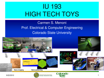
IU 193HIGH TECH TOYSCarmen S. MenoniProf. Electrical & Computer EngineeringColorado State UniversityExtreme Ultravioletlasers pticalstorageNano-imaging9/22/2010Nano-patterning1
Syllabus Course description:Students are introduced to the major scientific breakthroughs that havemade impact in many areas of science and technology. Emphasis will begiven to technologies that made possible the engineering of communicationnetworks like the internet. Key concepts of waves, light generation anddetection, optical and wireless communication will be covered. Othertechnologies that have revolutionized mankind will also be explored.Course credits:1Prerequisites:NoneCourse Goals: i) To make students appreciate technology and the sciencethat makes this technology possible in a way that is simple and intuitive; ii)to instill curiosity; iii) to develop communication skills through written andoral presentations; iv) to learn the use of the library and specialized searchengines. 9/22/20102
Syllabus Course Outline:1.2.3.4.5.6.9/22/2010Waves: what are they, how are they generated?Different types of waves: radio, microwave, light signals.Lasers- 50th anniversaryLasers in communication, medicine and industrySilicon technology and its impact.Students turn in their final report and hold their oral presentation3
Syllabus Homework: Homework will be assigned each week. It will consist of short research papersrelated to the class topics. Every Tuesday the New York Times publishes the ‘Science” section.Students will be required to pick an article of their choice related to advances in science andtechnology and write a short review ( 300 words). No late homework will be accepted.Research Paper: Students will form teams of up to three and research on a High Tech Toy oftheir interest. They will write an essay ( 1000 words) and compose a power-point presentationthat will be presented in class the last week of classes.In-class participation: Students will be expected to pro-actively contribute to discussions at thesmall group and whole class levels; to keep a notebook with up-to-date class notes; to beprepared for class with assignments and required class material. Short quizzes will be given.Additional Elective Activities: The instructor of this class has a strong appreciation for the artsand will share these interests with the students by inviting them to concerts organized by theMusic Department, Art exhibitions by the Art Department, and movies that are part of CSU ASAPCinema series.Grading:9/22/201060 % Homework15 % In-class participation – includes quiz grade25 % Research Paper – written and oral presentation4
How and where the InformationAge started? 1980 – Enquire -first program that linked bits of data– Tim Berner-Lee created at program at CERN (European Organization forNuclear Research) – Code was lost 1984 – Tangle – Berners-Lee created this program atCERN to keep track of many projects and incompatiblecomputers Computer Web code was written on and Web browserwas designed on:– NeXT – (founded by Steve Jobs-Apple Computers) – languageC – it took 3 months to write– Web browser: WorldWideWeb – could edit web pages andaccess them First server address– Nxoc01.cern.ch – with alias of info.cern.chScientific American, March 12, 2009, M. Fischetti9/22/20105
How and where the InformationAge started? First full demonstration– Christmas Day 1990, operating from Berners-LeeNeXT machine to the NeXT computer of his partnerand now Web-developer Robert Cailliau Content of first Web page:– The CERN phone directory Hits on the pages – August 1991: 100 a day- August 1993 –10,000 a day First U.S. Web server– April 1991, Stanford University Linear Accelerator LabScientific American, March 12, 2009, M. Fischetti9/22/20106
How and where the InformationAge started? First Web browsers– WorldWideWeb – Dec. 1990 – NeXT platform- Berners-Lee –– Erwise – April 1992 – UNIX platform –students at Helsinki University– Viola, May 1992 – student Pei Wei, UCBerkeley– Samba, Summer 1992 – Macintosh by RobertCaillau, CERN– Netscape, Yahoo, Google and Scientific American, March 12, 2009, M. Fischetti9/22/20107
What are the technologies that makepossible the World Wide Web? In class exercise: Students’ inputSatellitesFiber optics and lasersCablesComputersComputer programsProgramming languages and codesElectrical power9/22/20108
Mapping the internetNodes worldwide http://www.technologyreview.com/Infotech/18944/?a fThe shape of the online universe.This image shows the hierarchicalstructure of the Internet, based on theconnections between individual nodes(such as service providers). Threedistinct regions are apparent: an innercore of highly connected nodes, anouter periphery of isolated networks,and a mantle-like mass of peerconnected nodes. The bigger the node,the more connections it has. Thosenodes that are closest to the center areconnected to more well-connectednodes than are those on the periphery.Lanet-vi program of I. Alvarez-Hamelin et al.9/22/20109
Mapping the internetNodes worldwideThe core: At the center of theInternet are about 80 core nodesthrough which most traffic flows.Remove the core, and 70 percentof the other nodes are still able tofunction through peer-to-peerconnections.9/22/201010
Mapping the internetNodes worldwideThe periphery: At the veryedge of the Internet are 5,000or so isolated nodes that arethe most dependent upon thecore and become cut off if thecore is removed or shutdown. Yet those nodes withinthis periphery are able to stayconnected because of theirpeer-to-peer connections.9/22/201011
Providers red USA rnetmap labels 0.pdf9/22/201012
Global internet mapshttp://www.google.com/imgres?imgurl &imgrefurl etmap&usg DR4kglL1Fpopgi1TgwjZmcxxuoo &h 855&w 1200&sz 172&hl en&start 0&zoom 1&tbnid r4O51fwvMo Z9M:&tbnh 155&tbnw 218&prev %3Disch:1&um 1&itbs 1&iact rc&dur 468&ei gJmHTPrTE4SksQO8j6SMCg&oei gJmHTPrTE4SksQO8j6SMCg&esq 1&page 1&ndsp 23&ved 1t:429,r:0,s:0&tx 119&ty 939/22/201013
Week 2 Signals – how do one can transmitinformation?9/22/201014
Waves are perturbations of amedium in time and arkling waves/little-waves.jpg9/22/201015
There are different types of waves Waves are disturbances that transmitenergy from one point to another– Waves in ocean – water is the medium thatmoves– Sound waves –air moves– There are other types of waves that we cannot see them: ELECTROMAGNETIC WAVES Can not see them.9/22/201016
Electromagnetic Waves (theelectromagnetic spectrum) These waves originate from moving electrons They have been exploited in many applicationsLightRadarWeldingFiber g andpatterning (CSU)CAT scanimaging17
Electromagnetic Waves Electrons inside materials, or in gases can‘wiggle’ when electric forces are acting onthem.– http://phet.colorado.edu/simulations/sims.php?sim Radio Waves and Electromagnetic Fields9/22/201018
Waves Waves are characterized by–––––––––9/22/2010Wavelength ( )Frequency ( )Period - TAmplitudeSpeedEnergyPolarizationPhaseCoherence19
WavelengthAmplitude Distance between two crests of the waverrWavelength is measured inmeters or fractions of a meter9/22/201020
Waves can be periodic or aperiodicPeriodic wavespacePeriodicwaveAperiodic wave9/22/201021
For periodic waves, wecan identify a period, T,by measuring the timetaken for a wavelengthto pass a given point The frequency, , is theinverse of the period i.e. 1/T and is the number oftimes per second thatan oscillation occurs atany fixed point in space9/22/2010AmplitudePeriod and FrequencytimeTPeriod is measured in secondsor fractions of a secondFrequency is inverse of time ismeasured in Hertz.22
Prefixes used in units ofwavelength, Time and length(m)Time (sec) 59/22/2010fs23
Comparison of wavelengths across theelectromagnetic spectrum to other 4
Speedc: speed ofelectromagnetic signals invacuum is 3x10⁸ m/sAmplitude The speed of a wave is calculated fromthe distance it travels in one period ( )divided by the tions/sims.php?sim Wave Interference9/22/201025
Energy Waves carry energy –– Fluence in Joules per square cm is used tomeasure energy density– Intensity in Watts per square cm is used tomeasure power density9/22/201026
Polarization In electromagnetic signals the electric fieldoscillates in specific directions. This iscalled polarization. We exploit this to filterlight for example with plets/polarized.html9/22/201027
Phase and coherenceALL SIGNALS REACHMAXIMUM AT THESAME TIME ANDSAME LOCATION INSPACE – SIGNALSHAVE SAME PHASE.distanceTHESE SIGNALS ARECOHERENTThese two signals arenot in phase –They are INCOHERENT9/22/201028
Light emitters for communication systemsLIGHT EMITTING DIODES AND LASERS SOURCES OF MONOCHROMATIC (ONECOLOR) LIGHT POWERED BY ELECTRICITY OROTHER LIGHT SOURCES , THEYGENERATE LIGHT– LIGHT EMITTING DIODES: INCOHERENTLIGHT– LASERS –(Light Amplification by StimulatedEmission of Radiation): COHERENT LIGHT9/22/201029
LIGHT GENERATIONHow is light made?Material –could be agas, solid 10After some timeLight is emitted30
LIGHT GENERATION VIAELECTRICAL DISCHARGEGasFilamentLight outelectronatom- hp?sim Neon Lightsand Other Discharge Lamps9/22/201031
LIGHT EMITTING DIODESSolidmaterialcurrentLight out -batterySolid State Materials:semiconductors such as GaN, AlGaN9/22/201032
Applications: solid state lighteningRoadside illuminationLandscape illuminationLEDsconsumelesselectricityand lastmuchlonger thanlight-bulbshttp://www.osram-os.com9/22/201033
Applications: solid state lighteningCar designer Fioravanti’s Yak conceptvehicle demonstrates the potential of LEDstyle headlamps.Osram LEDs are prominent in this latestFord car.http://optics.orgElectronic Design May 13, 20029/22/201034
LASER: Principle of operationEnergyLight outmirrorsWith mirrors the light emitted ishighly directional and php?sim Lasers9/22/201035
Laser diodes used forcommunications They are small and efficient They operate in the infrared range (1.3-1.5m for long haul communications)9/22/201036
Laser diodes used forcommunications The emission wavelength of the laser isselected to minimize absorption anddispersion in the fiber optics that carry thesignal generated by the laserlengthAttenuation: amplitudeof pulse decreases as ittravels through the fiberDispersion: pulsebroadens in wavelengthsas it travels through thelength fiber9/22/201037
Fiber optics are glass cablescapable to transmit lightLight is transmitted by theprocess of total internalreflection. That is the light isreflected from the inner wallsof the -optic-communications/fiber-optic.htm9/22/201038
Fiber optics communicationsystemSignal inFiber spoolSignal outLaser diodeoutputmodulatedBandDescriptionWavelength RangeO bandoriginal1260 to 1360 nmE bandextended1360 to 1460 nmS bandshort wavelengths1460 to 1530 nmC bandconventional ("erbium window")1530 to 1565 nmL bandlong wavelengths1565 to 1625 nmU bandultralong wavelengths1625 to 1675 lifiers)DetectorPhotodiode39
Advantages of fiber -optic-communications/fiber-optic4.htm Less expensive - Several miles of optical cable can be made cheaper thanequivalent lengths of copper wire. This saves your provider (cable TV, Internet) andyou money. Thinner - Optical fibers can be drawn to smaller diameters than copper wire. Higher carrying capacity - Because optical fibers are thinner than copper wires,more fibers can be bundled into a given-diameter cable than copper wires. Thisallows more phone lines to go over the same cable or more channels to comethrough the cable into your cable TV box. Less signal degradation - The loss of signal in optical fiber is less than in copperwire. Light signals - Unlike electrical signals in copper wires, light signals from one fiberdo not interfere with those of other fibers in the same cable. This means clearerphone conversations or TV reception. Low power - Because signals in optical fibers degrade less, lower-power transmitterscan be used instead of the high-voltage electrical transmitters needed for copperwires. Again, this saves your provider and you money. Digital signals - Optical fibers are ideally suited for carrying digital information, whichis especially useful in computer networks. 9/22/2010Non-flammable - Because no electricity is passed through optical fibers, there is no 40fire hazard.
Network of fiber optics /201041
Other applications of fm Medicine– Surgery, dermatology Biology– Imaging/Microscopy Optics– Interferometry, holography, microscopy, spectroscopy Atmospheric science– Ranging and probing, LIDAR (light detection and ranging Materials science– Cutting, welding, engraving, cleaning, lithographyMovie from Laserfest9/22/201042
Lasers in medicine Optical Coherence novations.cfmOptical Coherence Tomography is like ultrasound. The laser light penetrates below surfaceof the human tissue and is reflected back. The laser reflection from the tissue is recordedback. An image is constructed from the data. Multiple scans over a region yields a 3-Dimage. Surgery– Eye surgery – Excimer lasers (UV) sculpt the cornea (LASIK) –Catarat removal– Blood-less surgery (green laser cauterizes/ ligates vessels as itcuts)9/22/201043
Lasers used in material scienceCeramic ProcessType of LaserWavelengthScribing, Drilling andProfiling Fired Substrates(Alumina, AlN, BeO)CO2Scribing, Drilling andProfiling Green SubstratesCO2/UV10.9/0.2 mDiodePumpedSolidStateSelective Material RemovalYAG/Green/UV-DPSSMarking/SerializingCO2 /YAG/Green/ UVDPSS10.9/1.06/0.52/0.24mLithographyExcimer0.197 m9/22/201010.9 m -10-100 W44
Lithography- How to make a Siliconchip Photolithography is the technology used to printsemiconductor chipsSystem is like a microscope. It formsa demagnified image of the maskSamsung Flash Memory 30 GbPrints 30 nm lines9/22/201045
Lithography is an ultra-cleanprocess In the US, Intel and GlobalFoundries(previously AMD) fabricate chipsCleanroomhttp://wn.com/Silicon Wafer Processing Animation9/22/201046
What controls size of the small featurethat can be printed? UV lithography is reaching its limits where k process dependent constant, NA is thenumerical aperture of the lens that focuses the light intothe wafer and creates the image of the mask NA of a lens can not be greater than 1. But it can beincreased using immersion. This is the way that currentchips with critical dimensions CD of 32 nm are preintedusing 196nm wavelength light from an excimer laser.9/22/201047
Moore’s lawThe number of transistors that can be placed inexpensively on anintegrated circuit has doubled approximately every two years9/22/201048
EUV Lithography will print 16nm featuresand below – In production in 2014 ASML making the printing tools with EUVsources engineered by CYMER – Printwavelength: 13.5 nm9/22/201049
Elements of Printing process Wafer: Silicon ultrapolished and flat Mask: Glass with a pattern of Cr that isfabricated with electron beam lithographyMaskAligner9/22/201050
The lithographic process Process to transfer the mask pattern into the wafer9/22/201051
Smallest periodic lines printedon resist using EUV Lithography Center of X-Ray Optics, LawrenceBerkeley lab. - SematechNm period lineson a mask areneeded to printthe gates oftransistors on achip9/22/201052
The transistorIn December 1947 three researchers demonstrated a device thatwould change the way humankind works and playsScientific American: The Solid-State Century, 1997Late 50’s1947Transistor is a device that can:Control current –(switch)Amplify current9/22/2010INVENTORS Shockley(seated), Bardeen (left) andBrattain (right) were thefirst to demonstrate a solidstate amplifier53
What transistors have enabled Vacuum tube technologyTransistor technologyAM/FM radio 2010AM/FM readio from 50’s9/22/201054
Transistors on a chip A transistor is used for switching, relaying, and amplifying electrical signals. In thehydraulic world, this would be equivalent to a valve that can be opened and closedwith a separate pressure input, with a second one-way check valve on the output sideof the assembly. As more pressure is applied onto the control line, more fluid isallowed to flow through the valves.METAL OXIDE FIELD EFFECTTRANSISTORBy applying avoltage to the gate,it is possible tocontrol the flow ofelectrons from thesource to the drainThis is theworkhorse of dataprocessing9/22/201055
Microprocessors (CPU) A collection of transistors, and other elements, such as resistors,capacitors diodes make up an electronic circuit or IC. A micro-processor is an IC that incorporatesfunctions. There is acomplex architecture design in the IC. The micro-processor or CPUis the heart of a computer.IBM RS/60009/22/201056
Microprocessors (CPU) Microprocessors can only receive and process data in the form of 0(no signal) or 1 (signal above a certain threshold). This is a BIT. All information to be processed by the microprocessor is firstdigitized and then converted into a binary signal. Decimal: 0123456789BCD: 0000 0001 0010 0011 0100 0101 0110 0111 1000 1001The INTEL 4004 was the first microprocessor – It consisted of a four–chiparchitectural with : a ROM (READ ONLY MEMORY) chip for storing theprograms, a dynamic RAM (RANDOM ACCESS MEMORY) chip for storingdata, a simple I/O device and a 4-bit central processing unit (CPU)9/22/201057
Microprocessor evolutionClock speed(maximum ratechip can beclockedData width(length of nibs)MIPS (Millions ofInstructions persecond)NameDateTransistorsMicrons (widthof transistorgate)808019746,00062 MHz8 bits0.648088197929,00035 MHz16 bits8-bit bus0.33802861982134,0001.56 MHz16 bits1803861985275,0001.516 MHz32 bits58048619891,200,000125 MHz32 bits20Pentium19933,100,0000.860 MHz32 bits64-bit bus100Pentium II19977,500,0000.35233 MHz32 bits64-bit bus 300Pentium III19999,500,0000.25450 MHz32 bits64-bit bus 510Pentium 4200042,000,0000.181.5 GHz32 bits64-bit bus 1,700Pentium 4"Prescott"2004125,000,0000.093.6 GHz32 bits64-bit bus 7,0009/22/2010Present technology inhigh volumemanufacturingGate width: 32 nm58
Intel newest ocessTransistorsAddressable MemoryCacheBusSpeedTypicalUseIntel Core 2ExtremeQ90002 GHzDec-0845nm410 million64 GB6 MB1066 MHzEnthusiastNotebookIntel Core 2DuoprocessorT98002.93 GHzDec-0845nm410 million64 GB6 MB1066 MHzMobile PC9/22/201059
9/22/2010 4 Homework: Homework will be assigned each week. It will consist of short research papers related to the class topics. Every Tuesday the New York Times publishes the ‘Science” section. Students will be