Transcription
chapter2.fm Page 33 Monday, September 4, 2000 11:11 AMCHAPTER2THE MANUFACTURING PROCESSOverview of manufacturing processnDesign rulesnIC packagingnFuture Trends in Integrated Circuit Technology2.1Introduction2.2Manufacturing CMOS Integrated Circuits2.5.1Short-Term Developments2.2.1The Silicon Wafer2.5.2In the Longer Term2.2.2Photolithography2.2.3Some Recurring Process Steps2.2.4Simplified CMOS Process Flow2.3Design Rules — The Contract betweenDesigner and Process Engineer2.4Packaging Integrated Circuits2.4.1Package Materials2.4.2Interconnect Levels2.4.3Thermal Considerations in Packaging2.52.6Perspective — Trends in Process TechnologySummary33
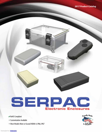
chapter2.fm Page 34 Monday, September 4, 2000 11:11 AM342.1THE MANUFACTURING PROCESSChapter 2IntroductionMost digital designers will never be confronted with the details of the manufacturing process that lies at the core of the semiconductor revolution. Yet, some insight in the stepsthat lead to an operational silicon chip comes in quite handy in understanding the physicalconstraints that are imposed on a designer of an integrated circuit, as well as the impact ofthe fabrication process on issues such as cost.In this chapter, we briefly describe the steps and techniques used in a modern integrated circuit manufacturing process. It is not our aim to present a detailed description ofthe fabrication technology, which easily deserves a complete course [Plummer00]. Ratherwe aim at presenting the general outline of the flow and the interaction between the various steps. We learn that a set of optical masks forms the central interface between theintrinsics of the manufacturing process and the design that the user wants to see transferred to the silicon fabric. The masks define the patterns that, when transcribed onto thedifferent layers of the semiconductor material, form the elements of the electronic devicesand the interconnecting wires. As such, these patterns have to adhere to some constraintsin terms of minimum width and separation if the resulting circuit is to be fully functional.This collection of constraints is called the design rule set, and acts as the contract betweenthe circuit designer and the process engineer. If the designer adheres to these rules, he getsa guarantee that his circuit will be manufacturable. An overview of the common designrules, encountered in modern CMOS processes, will be given. Finally, an overview isgiven of the IC packaging options. The package forms the interface between the circuitimplemented on the silicon die and the outside world, and as such has a major impact onthe performance, reliability, longevity, and cost of the integrated circuit.2.2Manufacturing CMOS Integrated CircuitsA simplified cross section of a typical CMOS inverter is shown in Figure 2.1. The CMOSprocess requires that both n-channel (NMOS) and p-channel (PMOS) transistors be builtin the same silicon material. To accomodate both types of devices, special regions calledwells must be created in which the semiconductor material is opposite to the type of thechannel. A PMOS transistor has to be created in either an n-type substrate or an n-well,while an NMOS device resides in either a p-type substrate or a p-well. The cross sectionFigure 2.1Cross section of an n-well CMOS process.
chapter2.fm Page 35 Monday, September 4, 2000 11:11 AMSection 2.2Manufacturing CMOS Integrated Circuits35shown in Figure 2.1 features an n-well CMOS process, where the NMOS transistors areimplemented in the p-doped substrate, and the PMOS devices are located in the n-well.Increasingly, modern processes are using a dual-well approach that uses both n- and pwells, grown on top on a epitaxial layer, as shown in Figure 2.2. We will restrict theremainder of this discussion to the latter process (without loss of generality).gate-oxideT i S i2A lCuSiO 2Tungstenpolyp-welln S iO 2n-wellp -e p ip p Figure 2.2Cross section of modern dual-well CMOS process.The CMOS process requires a large number of steps, each of which consists of asequence of basic operations. A number of these steps and/or operations are executed veryrepetitively in the course of the manufacturing process. Rather than diving directly into adescription of the overall process flow, we first discuss the starting material followed by adetailed perspective on some of the most-often recurring operations.2.2.1The Silicon WaferThe base material for the manufacturing process comesin the form of a single-crystalline, lightly doped wafer.These wafers have typical diameters between 4 and 12inches (10 and 30 cm, respectively) and a thickness ofat most 1 mm, and are obtained by cutting a singlecrystal ingot into thin slices (Figure 2.3). A startingwafer of the p--type might be doped around the levelsof 2 1021 impurities/m3. Often, the surface of thewafer is doped more heavily, and a single cristal epitaxial layer of the opposite type is grown over the surfacebefore the wafers are handed to the processing company. One important metric is the defect density of thebase material. High defect densities lead to a largerfraction of non-functional circuits, and consequently anincrease in cost of the final product.Figure 2.3 Single-crystal ingot andsliced wafers (from [Fullman]).
chapter2.fm Page 36 Monday, September 4, 2000 11:11 AM36THE MANUFACTURING PROCESS2.2.2Chapter 2PhotolithographyIn each processing step, a certain area on the chip is masked out using the appropriate optical mask so that a desired processing step can be selectively applied to the remainingregions. The processing step can be any of a wide range of tasks including oxidation, etching, metal and polisilicon deposition, and ion implantation. The technique to accomplishthis selective masking, called photolithography, is applied throughout the manufacturingprocess. Figure 2.4 gives a graphical overview of the different operations involved in atypical photolitographic process. The following steps can be identified:opticalmaskoxidationphotoresistremoval (ashing)photoresist coatingstepper exposureFigure 2.4 Typical operations in a singlephotolithographic cycle (from [Fullman]).photoresistdevelopmentacid etchprocessstepspin, rinse, dry1. Oxidation layering — this optional step deposits a thin layer of SiO2 over the complete wafer by exposing it to a mixture of high-purity oxygen and hydrogen at 1000 C. The oxide is used as an insulation layer and also forms transistor gates.2. Photoresist coating — a light-sensitive polymer (similar to latex) is evenly appliedwhile spinning the wafer to a thickness of approximately 1 µm. This material isoriginally soluble in an organic solvent, but has the property that the polymers crosslink when exposed to light, making the affected regions insoluble. A photoresist of
chapter2.fm Page 37 Monday, September 4, 2000 11:11 AMSection 2.2Manufacturing CMOS Integrated Circuits37this type is called negative. A positive photoresist has the opposite properties; originally insoluble, but soluble after exposure. By using both positive and negativeresists, a single mask can sometimes be used for two steps, making complementaryregions available for processing. Since the cost of a mask is increasing quite rapidlywith the scaling of technology, a reduction of the number of masks is surely of highpriority.3. Stepper exposure — a glass mask (or reticle), containing the patterns that we want totransfer to the silicon, is brought in close proximity to the wafer. The mask isopaque in the regions that we want to process, and transparent in the others (assuming a negative photoresist). The glass mask can be thought of as the negative of onelayer of the microcircuit. The combination of mask and wafer is now exposed toultra-violet light. Where the mask is transparent, the photoresist becomes insoluble.4. Photoresist development and bake — the wafers are developed in either an acid orbase solution to remove the non-exposed areas of photoresist. Once the exposedphotoresist is removed, the wafer is "soft-baked" at a low temperature to harden theremaining photoresist.5. Acid Etching — material is selectively removed from areas of the wafer that are notcovered by photoresist. This is accomplished through the use of many differenttypes of acid, base and caustic solutions as a function of the material that is to beremoved. Much of the work with chemicals takes place at large wet benches wherespecial solutions are prepared for specific tasks. Because of the dangerous nature ofsome of these solvents, safety and environmental impact is a primary concern.6. Spin, rinse, and dry — a special tools (called SRD) cleans the wafer with deionizedwater and dries it with nitogen. The microscopic scale of modern semiconductordevices means that even the smallest particle of dust or dirt can destroy the circuitry.To prevent this from happening, the processing steps are performed in ultra-cleanrooms where the number of dust particles per cubic foot of air ranges between 1 and10. Automatic wafer handling and robotics are used whenever possible. Thisexplains why the cost of a state-of-the-art fabrication facility easily ranges in themultiple billions of dollars. Even then, the wafers must be constantly cleaned toavoid contamination, and to remove the left-over of the previous process steps.7. Various process steps — the exposed area can now be subjected to a wide range ofprocess steps, such as ion implantation, plasma etching, or metal deposition. Theseare the subjects of the subsequent section.8. Photoresist removal (or ashing) — a high-temperature plasma is used to selectivelyremove the remaining photoresist without damaging device layers.We illustrate the use of the photolitographic process for one specific example, thepatterning of a layer of SiO2, in Figure 2.5. The sequence of process steps shown in theFigure patterns exactly one layer of the semiconductor material, and may seem very complex. Yet, the reader has to bear in mind that that same sequence patterns the layer of thecomplete surface of the wafer. It is hence a very parallel process, transferring hundredsof millions of patterns to the semiconductor surface simultaneously. The concurrent and
chapter2.fm Page 38 Monday, September 4, 2000 11:11 AM38THE MANUFACTURING PROCESSChapter 2Chemical or plasmaetchSi-substrateHardened resistSiO2(a) Silicon base materialSi-substratePhotoresistSiO2Si-substrate(d) After development and etching of resist,chemical or plasma etch of SiO2Hardened resistSiO2(b) After oxidation and depositionof negative photoresistSi-substrateUV-lightPatternedoptical mask(e) After etchingExposed resistSi-substrate(c) Stepper exposureSiO2Si-substrate(f) Final result after removal of resistFigure 2.5 Process steps for patterning of SiO 2.scalable nature of the optolithographical process is what makes the cheap manufacturingof complex semiconductor circuits possible, and lies at the core of the economic successof the semiconductor industry.The continued scaling of the minimum feature sizes in integrated circuits puts anenormous burden on the developer of semiconductor manufacturing equipment. This isespecially true for the optolithographical process. The dimensions of the features to betranscribed approach the wavelengths of the optical light sources, so that achieving thenecessary resolution and accuracy becomes harder and harder. So far, ingenous ingeneering has extended the lifetime of this process at least until the 100 nm (or 0.1 µm) processgeneration. Beyond that point, other solutions that offer a a finer resolution such as X-rayor electron-beam may be needed. These techniques, while fully functional, are currentlyless attractive from an economic viewpoint.
chapter2.fm Page 39 Monday, September 4, 2000 11:11 AMSection 2.22.2.3Manufacturing CMOS Integrated Circuits39Some Recurring Process StepsDiffusion and Ion ImplantationMany steps of the integrated circuit manufacturing process require a chance in thedopant concentration of some parts of the material. The creation of the source and drainregions, well and substrate contacts, the doping of the polysilicon, and the adjustments ofthe device threshold are examples of such. There exist two approaches for introducingthese dopants—diffusion and ion implantation. In both techniques, the area to doped isexposed, while the rest of the wafer is coated with a layer of buffer material, typicallySiO2.In diffusion implantation, the wafers are placed in a quartz tube embedded in aheated furnace. A gas containing the dopant is introduced in the tube. The high temperatures of the furnace, typically 900 to 1100 C, cause the dopants to diffuse into theexposed surface both vertically and horizontally. The final dopant concentration is thegreatest at the surface and decreases in a gaussian profile deeper in the material.In ion implantation, dopants are introduced as ions into the material. The ionimplantation system directs and sweeps a beam of purified ions over the semiconductorsurface. The acceleration of the ions determines how deep they will penetrate the material,while the beam current and the exposure time determine the dosage. The ion implantationmethod allows for an independent control of depth and dosage. This is the reason that ionimplantation has largely displaced diffusion in modern semiconductor manufacturing.Ion implantation has some unfortunate side effects however, the most important onebeing lattice damage. Nuclear collisions during the high energy implantation cause thedisplacement of substrate atoms, leading to material defects. This problem is largelyresolved by applying a subsequent annealing step, in which the wafer is heated to around1000 C for 15 to 30 minutes, and then allowed to cool slowly. The heating step thermallyvibrates the atoms, which allows the bonds to reform.DepositionAny CMOS process requires the repetitive deposition of layers of a material overthe complete wafer, to either act as buffers for a processing step, or as insulating or conducting layers. We have already discussed the oxidation process, which allows a layer ofSiO2 to be grown. Other materials require different techniques. For instance, siliconnitride (Si3N4) is used as a sacrificial buffer material during the formation of the fieldoxide and the introduction of the stopper implants. This silicon nitride is deposited everywhere using a process called chemical vapor deposition or CVD, which uses a gas-phasereaction with energy supplied by heat at around 850 C.Polysilicon, on the other hand, is deposited using a chemical deposition process,which flows silane gas over the heated wafer coated with SiO2 at a temperature of approximately 650 C. The resulting reaction produces a non-cristalline or amorphous materialcalled polysilicon. To increase to conductivity of the material, the deposition has to be followed by an implantation step.The Aluminum interconnect layers are typically deployed using a process known assputtering. The aluminum is evaporated in a vacuum, with the heat for the evaporation
chapter2.fm Page 40 Monday, September 4, 2000 11:11 AM40THE MANUFACTURING PROCESSChapter 2delivered by electron-beam or ion-beam bombarding. Other metalic interconnect materialssuch as Copper require different deposition techniques.EtchingOnce a material has been deposited, etching is used to selectively form patterns suchas wires and contact holes. The wet etching process was described earlier, and makes useof acid acid or basic solutions. For instance, hydrofluoric acid buffered with ammoniumfluoride is typically used to etch SiO2.In recent years, dry or plasma etching has made a lot of inroad. A wafer is placedinto the etch tool's processing chamber and given a negative electrical charge. The chamber is heated to 100 C and brought to a vacuum level of 10 millitorrs, then filled with apositively charged plasma (usually a mix of nitrogen, chlorine and boron trichloride). Theopposing electrical charges cause the rapidly moving plasma molecules to align themselves in a vertical direction, forming a microscopic chemical and physical "sandblasting"action which removes the exposed material. Plasma etching has the advantage of offeringa well-defined directionality to the etching action, creating patterns with sharp verticalcontours.PlanarizationTo reliably deposit a layer of material onto the semiconductor surface, it is essentialthat the surface is approximately flat. If no special steps were taken, this would definitelynot be the case in modern CMOS processes, where multiple patterned metal interconnectlayers are superimposed onto each other. Therefore, a chemical-mechanical planarization(CMP) step is included before the deposition of an extra metal layer on top of the insulating SiO2 layer. This process uses a slurry compound—a liquid carrier with a suspendedabrasive component such as aluminum oxide or silica—to microscopically plane a devicelayer and to reduce the step heights.2.2.4Simplified CMOS Process FlowThe gross outline of a potential CMOS process flow is given in Figure 2.6. The processstarts with the definition of the active regions, this is the regions where transistors will beconstructed. All other areas of the die will be covered with a thick layer of silcion dioxide(SiO2), called the field oxide. This oxide acts as the insulator between neighboringdevices, and is either grown (as in the process of Figure 2.1), or deposited in etchedtrenches (Figure 2.2) — hence the name trench insulation. Further insulation is providedby the addition of a reverse-biased np-diode, formed by adding an extra p region, calledthe channel-stop implant (or field implant) underneat the field oxide. Next, lightly dopedp- and n-wells are formed through ion implantation. To construct an NMOS transistor in ap-well, heavily doped n-type source and drain regions are implanted (or diffused) into thelightly doped p-type substrate. A thin layer of SiO2, called the gate oxide, separates theregion between the source and drain, and is itself covered by conductive polycrystallinesilicon (or polysilicon, for short). The conductive material forms the gate of the transistor.PMOS transistors are constructed in an n-well in a similar fashion (just reverse n’s and
chapter2.fm Page 41 Monday, September 4, 2000 11:11 AMSection 2.2Manufacturing CMOS Integrated Circuits41Define active areasEtch and fill trenchesImplant well regionsDeposit and patternpolysilicon layerImplant source and drainregions and substrate contactsCreate contact and via windowsDeposit and pattern metal layersFigure 2.6 Simplified process sequence for the manufacturing of a ndual-well CMOS circuit.p’s). Multiple insulated layers of metalic (most often Aluminum) wires are deposited ontop of these devices to provide for the necessary interconnections between the transistors.A more detailed breakdown of the flow into individual process steps and theirimpact on the semiconductor material is shown graphically in Figure 2.7. While most ofthe operations should be self-explanatory in light of the previous descriptions, some comments on individual operations are worthwhile. The process starts with a p-substrate surfaced with a lightly doped p-epitaxial layer (a). A thin layer of SiO2 is deposited, whichwill serve as the gate oxide for the transistors, followed by a deposition of a thicker sacrificial silicon nitride layer (b). A plasma etching step using the complimentary of the activearea mask creates the trenches, used for insulating the devices (c). After providing thechannel stop implant, the trenches are filled with SiO2 followed by a nyumber of steps toprovide a flat surface (including inverse active pattern oxide etching, and chemicalmechanical planarization). At that point, the sacrificial nitride is removed (d). The n-wellmask is used to expose only the n-well areas (the rest of the wafer is covered by a thichbuffer material), after whihc an implant-annealing sequence is applied to adjust the welldoping. This is followed by a second implant step to adjust the threshold voltages of thePMOS transistors. This implant only impacts the doping in the area just below the gateoxide (e). Similar operations (using other dopants) are performed to created the p-wells,and to adjust the thresholds of the NMOS transistors (f). A thin layer of polysilicon ischemically deposited, and patterned with the aid of the polysilicon mask. Polysilicon isused both as gate electrode material for the transistors as well as an interconnect medium(g). Consecutive ion implantations are used to dope the source and drain regions of thePMOS (p ) and NMOS (n ) transistors, respectively (h), after which the thin gate oxidenot covered by the polysilicon is etched away1. The same implants are also use to dope the1Most modern processes also include extra implants for the creation of the lightly-doped drain regions(LDD), and the creation of gate spacers at this point. We have omitted these for the sake of simplicity.
chapter2.fm Page 42 Monday, September 4, 2000 11:11 AM42THE MANUFACTURING PROCESSp-epipChapter 2(a) Base material: p substratewith p-epi layer Si3N4SiO2p-epip (b) After deposition of gate-oxide andsacrificial nitride (acts as abuffer layer)(c) After plasma etch of insulatingtrenches using the inverse ofthe active area maskp SiO2(d) After trench filling, CMPplanarization, and removal ofsacrificial nitriden(e) After n-well andVTp adjust implantsp(f) After p-well andVTn adjust implants
chapter2.fm Page 43 Monday, September 4, 2000 11:11 AMSection 2.2Manufacturing CMOS Integrated Circuits43poly(silicon)(g) After polysilicon depositionand etchn p (h) After n source/drain andp source/drain implants. Thesesteps also dope the polysilicon.SiO2(i) After deposition of SiO2insulator and contact hole etch.Al(j) After deposition andpatterning of first Al layer.AlSiO2(k) After deposition of SiO2insulator, etching of via’s,deposition and patterning ofsecond layer of Al.Figure 2.7 Process flow for the fabrication of an NMOS and a PMOS transistor in a dual-well CMOS process. Beaware that the drawings are stylized for understanding, and that the aspects ratios are not proportioned to reality.
chapter2.fm Page 44 Monday, September 4, 2000 11:11 AM44THE MANUFACTURING PROCESSChapter 2polysilion on the surface, reducing its resistivity. Undoped polysilicon has a very highresistivity. Note that the polysilicon gate , which is patterned before the doping, actuallydefines the precise location of the channel region, and hence the location of the source anddrain regions. This procedure allows for a very precise positioning of the two regions relative to the gate, and hence is called the self-aligned process. The process continues withthe deposition of the metalic interconnect layers. These consists of a repition of the following steps (i-k): deposition of the insulating material (most often Si02), etching of thecontact or via holes, deposition of the metal (most often Aluminum, although Tungsten isoften used for the lower layers), and patterning of the metal. Intermediate planarizationsteps ensure that the surface remains reasonable flat, even in the presence of multipleinterconnect layers. After the last level of metal is deposited, a final passivation or overglass is deposited for protection. The layer would be CVD SiO2, although often an additional layer of nitride is deposited as it is more impervious to moisture. The finalprocessing step is to etch openings to the pads used for bonding.A cross-section of the final artifact is shown in Figure 2.8. Observe how the transistors occupy only a small fraction of the total height of the structure. The interconnect layers take up the majority of the vertical dimension.transistorFigure 2.8 Cross-section of state-of-the-artCMOS process.2.3Design Rules — The Contract between Designer and Process EngineerAs processes become more complex, requiring the designer to understand the intricaciesof the fabrication process and interpret the relations between the different masks is a sureroad to trouble. The goal of defining a set of design rules is to allow for a ready translationof a circuit concept into an actual geometry in silicon. The design rules act as the interfaceor even the contract between the circuit designer and the process engineer.Circuit designers in general want tighter, smaller designs, which lead to higher performance and higher circuit density. The process engineer, on the other hand, wants areproducible and high-yield process. Design rules are, consequently, a compromise thatattempts to satisfy both sides.
chapter2.fm Page 45 Monday, September 4, 2000 11:11 AMSection 2.3Design Rules — The Contract between Designer and Process Engineer45The design rules provide a set of guidelines for constructing the various masksneeded in the patterning process. They consist of minimum-width and minimum-spacingconstraints and requirements between objects on the same or on different layers.The fundamental unity in the definition of a set of design rules is the minimum linewidth. It stands for the minimum mask dimension that can be safely transferred to thesemiconductor material. In general, the minimum line width is set by the resolution of thepatterning process, which is most commonly based on optical lithography. More advancedapproaches use electron-beam or X-ray sources that offer a finer resolution, but are lessattractive from an economical viewpoint.Even for the same minimum dimension, design rules tend to differ from company tocompany, and from process to process. This makes porting an existing design between different processes a time-consuming task. One approach to address this issue is to useadvanced CAD techniques, which allow for migration between compatible processes.Another approach is to use scalable design rules. The latter approach, made popular byMead and Conway [Mead80], defines all rules as a function of a single parameter, mostoften called λ. The rules are chosen so that a design is easily ported over a cross section ofindustrial processes. Scaling of the minimum dimension is accomplished by simplychanging the value of λ. This results in a linear scaling of all dimensions. For a given process, λ is set to a specific value, and all design dimensions are consequently translated intoabsolute numbers. Typically, the minimum line width of a process is set to 2λ. Forinstance, for a 0.25 µm process (i.e., a process with a minimum line width of 0.25 µm), λequals 0.125 µm.This approach, while attractive, suffers from some disadvantages:1. Linear scaling is only possible over a limited range of dimensions (for instance,between 0.25 µm and 0.15 µm). When scaling over larger ranges, the relationsbetween the different layers tend to vary in a nonlinear way that cannot be adequately covered by the linear scaling rules.2. Scalable design rules are conservative. As they represent a cross section over different technologies, they have to represent the worst-case rules for the whole set. Thisresults in overdimensioned and less-dense designs.For these reasons, scalable design rules are normally avoided by industry. As circuit density is a prime goal in industrial designs, most semiconductor companies tend to usemicron rules, which express the design rules in absolute dimensions and can thereforeexploit the features of a given process to a maximum degree. Scaling and porting designsbetween technologies under these rules is more demanding and has to be performed eithermanually or using advanced CAD tools.For this textbook, we have selected a “vanilla” 0.25 µm CMOS process as our preferred implementation medium. The rest of this section is devoted to a short introductionand overview of the design rules of this process, which fall in the micron-rules class. Acomplete design-rule set consists of the following entities: a set of layers, relationsbetween objects on the same layer, and relations between objects on different layers. Wediscuss each of them in sequence.
chapter2.fm Page 46 Monday, September 4, 2000 11:11 AM46THE MANUFACTURING PROCESSChapter 2Layer RepresentationThe layer concept translates the intractable set of masks currently used in CMOS into asimple set of conceptual layout levels that are easier to visualize by the circuit designer.From a designer’s viewpoint, all CMOS designs are based on the following entities: Substrates and/or wells, being p-type (for NMOS devices) and n-type (for PMOS) Diffusion regions (n and p ) defining the areas where transistors can be formed.These regions are often called the active areas. Diffusions of an inverse type areneeded to implement contacts to the wells or to the substrate. These are called selectregions. One or more polysilicon layers, which are used to form the gate electrodes of thetransistors (but serve as interconnect layers as well). A number of metal interconnect layers. Contact and via layers to provide interlayer connections.A layout consists of a combination of polygons, each of which is attached to a certainlayer. The functionality of the circuit is determined by the choice of the layers, as well asthe interplay between objects on different layers. For instance, an MOS transistor isformed by the cross section of the diffusion layer and the polysilicon layer. An interconnection between two metal layers is formed by a cross section between the two metal layers and an additional contact layer. To visualize these relations, each layer is assigned astandard color (or stipple pattern for a black-and-white representation). The different layers used in our CMOS process are represented in Colorplate 1 (color insert).Intralayer ConstraintsA first set of rules defines the minimum dimensions of objects on each layer, as well as theminimum spacings between objects on the same layer. All distances are expressed in µm.These constraints are presented in a pictorial fashion in Colorplate 2.Interlayer ConstraintsThese rules tend to be more complex. The fact that multiple layers are involv
Section 2.2 Manufacturing CMOS Integrated Circuits 35 shown in Figure 2.1 features ann-well CMOS process, where the NMOS transistors are implemented in thep-doped substrate, and the PMOS devices are located in the n-well. Increasingly, modern processes are using adual-well approach that uses bothn- and p- wells, g