Transcription
MIPS Assembly Language ProgrammingRobert BrittonComputer Science DepartmentCalifornia State University, ChicoChico, California
Instructors are granted permission to make copies of this beta version textbook for use bystudents in their courses. Title to and ownership of all intellectual property rights in thisbook are the exclusive property of Robert Britton, Chico, California.ii
PrefaceThis book is targeted for use in an introductory lower-division assembly languageprogramming or computer organization course. After students are introduced to the MIPSarchitecture using this book, they will be well prepared to go on to an upper-divisioncomputer organization course using a textbook such as “Computer Organization andDesign” by Patterson and Hennessy. This book provides a technique that will make MIPSassembly language programming a relatively easy task as compared to writing complexIntel 80x86 assembly language code. Students using this book will acquire anunderstanding of how the functional components of computers are put together, and howa computer works at the machine language level. We assume students have experience indeveloping algorithms, and running programs in a high-level language.Chapter 1 provides an introduction to the basic MIPS architecture, which is a modernReduced Instruction Set Computer (RISC). Chapter 2 shows how to develop codetargeted to run on a MIPS processor using an intermediate pseudocode notation similar tothe high-level language “C”, and how easy it is to translate this notation to MIPSassembly language.Chapter 3 is an introduction to the binary number system, and the rules for performingarithmetic, as well as detecting overflow. Chapter 4 explains the features of the PCSpimsimulator for the MIPS architecture, which by the way is available for free. Within theremaining chapters, a wealth of programming exercises are provided, which everystudent needs to become an accomplished assembly language programmer. Instructorsare provided with a set of PowerPoint slides. After students have had an opportunity todevelop their pseudocode and their MIPS assembly language code for each of theexercises, they can be provided with example solutions via the PowerPoint slides.In Chapter 5 students are presented with the classical I/O algorithms for decimal andhexadecimal representation. The utility of logical operators and shift operators arestressed. In Chapter 6, a specific argument passing protocol is defined. Most significantprogramming projects are a teamwork effort. Emphasis is placed on the importance thateveryone involved in a teamwork project must adopt the same convention for parameterpassing. In the case of nested function calls, a specific convention is defined for savingand restoring values in the temporary registers. In Chapter 7 the necessity for reentrantcode is explained, as well as the rules one must follow to write such functions. Chapter 8introduces exceptions and exception processing. In Chapter 9 a pipelined implementationof the MIPS architecture is presented, and the special programming considerationsdealing with delayed loads and delayed branches are discussed. The final chapter brieflydescribes the expanding opportunities in the field of embedded processors forprogrammers who have a solid understanding of the underlying processor functionality.Robert BrittonMay 2002iii
ContentsCHAPTER 1: The MIPS Architecture. 11.1Introduction. 11.2The Datapath Diagram. 11.3Instruction Fetch and Execute. 21.4The MIPS Register File . 31.5The Arithmetic and Logic Unit (ALU). 31.6The Program Counter (PC) . 41.7Memory. 51.8The Instruction Register (IR) . 51.9The Control Unit . 51.10 Instruction Set . 61.11 Addressing Modes . 71.12 Summary. 8Exercises . 8CHAPTER 2: Pseudocode . 92.1Introduction. 92.2Develop the Algorithm in Pseudocode . 92.3Register Usage Convention. 122.4The MIPS Instruction Set. 122.5Translation of an “IF THEN ELSE” Control Structure . 132.6Translation of a “WHILE” Control Structure. 142.7Translation of a “FOR LOOP” Control Structure. 142.8Translation of Arithmetic Expressions . 152.9Translation of a “SWITCH” Control Structure . 162.10 Assembler Directives . 172.11 Input and Output . 18Exercises . 18CHAPTER 3: Number Systems. 213.1Introduction. 213.2Positional Notation. 213.3Converting Binary Numbers to Decimal Numbers. 223.4Detecting if a Binary Number is Odd or Even. 223.5Multiplication by Constants that are a Power of Two . 233.6The Double and Add Method . 233.7Converting Decimal Numbers to Binary Numbers. 243.8The Two’s Complement Number System. 243.9The Two’s Complement Operation . 253.10 A Shortcut for Finding the Two’s Complement of any Number . 253.11 Sign Extension . 263.12 Binary Addition . 263.13 Binary Subtraction . 263.14 Overflow Detection. 273.15 Hexadecimal Numbers. 27iv
Exercises . 28CHAPTER 4: PCSpim The MIPS Simulator. 314.1Introduction. 314.2Advantages of a Simulator. 314.3The Big Picture . 324.4Analyzing the Text Segment. 344.5Analyzing the Data Segment . 354.6System I/O . 364.7Deficiencies of the System I/O Services. 36Exercises . 38CHAPTER 5: Algorithm Development . 395.1Introduction. 395.2Instructions that Perform Logical Operations. 395.3Instructions that Perform Shift Operations . 415.4Modular Program Design and Documentation . 425.5A Function to Print Values in Hexadecimal Representation . 475.6A Function to Read Values in Hexadecimal Representation. 485.7A Function to Print Decimal Values Right Justified . 495.8A Function to Read Decimal Values and Detect Errors . 49Exercises . 50CHAPTER 6: Function Calls Using the Stack . 536.1Introduction. 536.2The Stack Segment in Memory. 536.3Argument Passing Convention . 536.4Nested Function Calls and Leaf Functions . 546.5Local Variables are Allocated Space on the Stack . 556.6Frame Pointer. 55Exercises . 56CHAPTER 7: Reentrant Functions. 597.1Introduction. 597.2Rules for Writing Reentrant Code . 597.3Reentrant I/O Functions. 607.4Personal Computers . 607.5Recursive Functions. 60Exercises . 61CHAPTER 8: Exception Processing. 638.1Introduction. 638.2The Trap Handler. 63Exercises . 65CHAPTER 9: A Pipelined Implementation. 679.1Introduction. 679.2A Pipelined Datapath . 689.3PCSpim Option to Simulate a Pipelined Implementation. 69Exercises . 69v
CHAPTER 10: Embedded Processors . 7110.1 Introduction. 7110.2 Code Development for Embedded Processors. 7110.3 Memory Mapped I/O . 7210.4 References. 72APPENDIX A: Quick Reference. 73APPENDIX B: ASCII Codes. 77APPENDIX C: Integer Instruction Set . 79APPENDIX D: Macro Instructions . 95APPENDIX E: A Trap Handler. 100Related Web Siteswww.mips.com/http://www.ecst.csuchico.edu/ brittonhttp://www.cs.wisc.edu/ ter.asphttp://www.cs.wisc.edu/ larus/SPIM/cod-appa.pdfvi
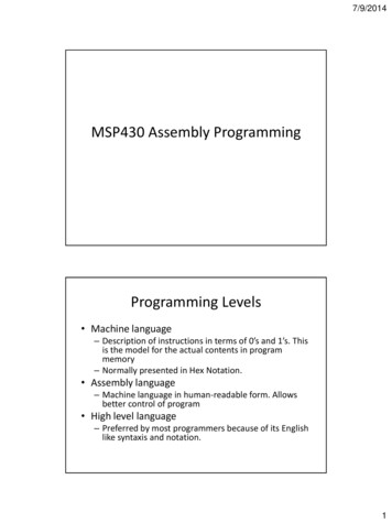
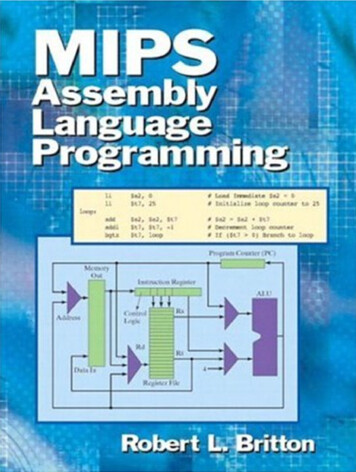
CHAPTER 1The MIPS ArchitectureIf at first you don’t succeed,Skydiving is definitely not for you.1.1IntroductionThis book provides a technique that will make MIPS assembly language programming arelatively easy task as compared to writing Intel 80x86 assembly language code. Weare assuming that you have experience in developing algorithms, and running programsin some high level language such as Pascal, C, C , or JAVA. One of the benefits ofunderstanding and writing assembly language code is that you will have new insights intohow to write more efficient, high-level language code. You will become familiar with thetask that is performed by a compiler and how computers are organized down to the basicfunctional component level. You may even open new opportunities for yourself in theexploding field of embedded processors.The first thing everyone must do to apply this technique is to become familiar with theMIPS architecture. The architecture of any computer is defined by the registers that areavailable (visible) to the assembly language programmer, the instruction set, the memoryaddressing modes, and the data types.1.2The Datapath DiagramIt is very useful to have a picture of a datapath diagram that depicts the essentialcomponents and features of the MIPS architecture. Please note that there are manydifferent ways that an architecture can be implemented in hardware. These days,pipelined and superscalar implementations are common in high-performance processors.An initial picture of a MIPS datapath diagram will be the straightforward simple diagramshown in Figure 1.1. This is not a completely accurate diagram for the MIPS architecture;it is just a useful starting point.1
Program Counter (PC)MemoryOutAddressInstruction RegisterALUControlLogicRdRsRt4Data InRegister FileFigure 1.1 MIPS Simplified Datapath Diagram1.3Instruction Fetch and ExecuteComputers work by fetching machine language instructions from memory, decoding andexecuting them. Machine language instructions and the values that are operated upon areencoded in binary. Chapter 3 introduces the binary number system. As we progressthrough the first two chapters, we will be expressing values as decimal values, but keepin mind that in an actual MIPS processor these values are encoded in binary. The basicfunctional components of the MIPS architecture shown in Figure 1.1 are:(a)Program Counter (PC)(b)Memory(c)Instruction Register (IR)(d)Register File(e)Arithmetic and Logic Unit (ALU)(f)Control UnitInterconnecting all of these components, except the control unit, are busses. A bus isnothing more than a set of electrical conducting paths over which different sets of binaryvalues are transmitted. Most of the busses in the MIPS architecture are 32-bits wide. Inother words, 32 separate, tiny wires running from a source to a destination.2
In this datapath diagram, we have the situation where we need to route information frommore than one source to a destination, such as the ALU. One way to accomplish this iswith a multiplexer. Multiplexers are sometimes called data selectors. In Figure 1.1,multiplexers are represented by the triangle-shaped symbols. Every multiplexer with twoinput busses must have a single control signal connected to it. This control signal comesfrom the control unit. The control signal is either the binary value zero or one, which issent to the multiplexer over a single wire. In Figure 1.1, we have not shown any of thecontrol signals, because it would make the diagram too busy. When the control signal iszero, the 32-bit value connected to input port zero (0) of the multiplexer will appear onthe output of the multiplexer. When the control signal is one, the 32-bit value connectedto input port one (1) of the multiplexer will appear on the output of the multiplexer. Theacronym “bit” is an abbreviation of “binary digit.”1.4The MIPS Register FileThe term “register” refers to an electronic storage component. Every register in the MIPSarchitecture is a component with a capacity to hold a 32-bit binary number. Anyone whohas ever used an electronic hand-held calculator has experienced the fact that there issome electronic component inside the calculator that holds the result of the latestcomputation.The MIPS architecture has a register file containing 32 registers. See Figure 1.2. Eachregister has a capacity to hold a 32-bit value. The range of values that can be representedwith 32 bits is -2,147,483,648 to 2,147,483,647. When writing at the assembly languagelevel almost every instruction requires that the programmer specify which registers in theregister file are used in the execution of the instruction. A convention has been adoptedthat specifies which registers are appropriate to use in specific circumstances. Theregisters have been given names that help to remind us about this convention. Register zero is special; it is the source of the constant value zero. Nothing can be stored inregister zero. Register number 1 has the name at, which stands for assemblertemporary. This register is reserved to implement “macro instructions” and should not beused by the assembly language programmer. Registers k0 and k1 are used by thekernel of the operating system and should not be changed by a user program.1.5The Arithmetic and Logic Unit (ALU)The ALU, as its name implies, is a digital logic circuit designed to perform binaryarithmetic operations, as well as binary logical operations such as “AND,” “OR,” and“Exclusive OR.” Which operation the ALU performs depends upon the operation code inthe Instruction Register.3
2728293031ValueName0 zero at v0 v1 a0 a1 a2 a3 t0 t1 t2 t3 t4 t5 t6 t7 s0 s1 s2 s3 s4 s5 s6 s7 t8 t9 k0 k1 gp sp fp raFigure 1.2 The Register File1.6The Program Counter (PC)After a programmer has written a program in assembly language using a text editor, themnemonic representation of the program is converted to machine language by a utilityprogram called an assembler. The machine language code is stored in a file on disk.When someone wants to execute the program, another utility program, called a linkingloader, loads and links together all of the necessary machine language modules into mainmemory. The individual instructions are stored sequentially in memory. The ProgramCounter (PC) is a register that is initialized by the operating system to the address of the4
first instruction of the program in memory. Notice in Figure 1.1 that the address in theprogram counter is routed to the address input of the memory via a bus. After aninstruction has been fetched from memory and loaded into the instruction register (IR),the PC is incremented so that the CPU will have the address of the next sequentialinstruction for the next instruction fetch. The name Program Counter is misleading. Abetter name would be Program Pointer, but unfortunately the name has caught on, andthere is no way to change this tradition.1.7MemoryMost modern processors are implemented with cache memory. Cache memory is locatedon the CPU chip. Cache memory provides fast memory access to instructions and datathat were recently accessed from the main memory. How cache memory is implementedin hardware is not the subject of this text. For our purposes, the functionality of cachememory will be modeled as a large array of locations where information is stored andfrom which information can be fetched, one “word” at a time, or stored one “word” at atime. The term “word” refers to a 32-bit quantity. Each location in memory has a 32-bitaddress. In the MIPS architecture, memory addresses range from 0 to 4,294,967,295. TheMIPS architecture specifies that the term “word” refers to a 32-bit value and the term“byte” refers to an 8-bit value. The MIPS architecture specifies that a word contains fourbytes, and that the smallest addressable unit of information that can be referenced inmemory is a byte. The address of the first byte in a word is also the address of the 32-bitword. All instructions in the MIPS architecture are 32 bits in length. Therefore, theprogram counter is incremented by four after each instruction is fetched.1.8The Instruction Register (IR)The Instruction Register (IR) is a 32-bit register that holds a copy of the most recentlyfetched instruction. In the MIPS architecture three different instruction formats aredefined, R - format, I - format, and J – format. (See Appendix C for details)1.9The Control UnitTo fetch and execute instructions, control signals must be generated in a specificsequence to accomplish the task. As you have already learned, multiplexers must havecontrol signals as inputs. Each register has an input control line, which when activatedwill cause a new value to be loaded into the register. The ALU needs control signals tospecify what operation it should perform. The cache memory needs control signals tospecify when a read or write operation is to be performed. The register file needs acontrol signal to specify when a value should be written into the register file. All of thesecontrol signals come from the control unit. The control unit is implemented in hardwareas a “finite state machine.” How fast the computer runs is controlled by the clock rate.The clock generator is an oscillator that produces a continuous waveform as depicted in5
Figure 1.3. The clock period is the reciprocal of the clock frequency. All moderncomputers run with clock rates in the mega-hertz (MHz) range. ( Mega 106 )Figure 1.3 Clock Waveform1.10 Instruction SetRefer to Appendix C for a list of the basic integer instructions for the MIPS Architecturethat we will be concerned with in this introductory level textbook. Note that uniquebinary codes assigned to each of the instructions. For a complete list of MIPSinstructions, a good reference is the book by Kane and Heinrich “MIPS RISCArchitecture.” In reviewing the list of instructions in Appendix C you will find that themachine has instructions to add and subtract. The operands (source values) for theseoperations come from the register file and the results go to the register file. Whenprogramming in assembly language we use a mnemonic to specify which operation wewant the computer to perform and we specify the register file locations using the namesof the register file locations. Let us suppose that an assembly language programmer wantsto add the contents of register a1 to the contents of register s1, and to place the resultsin register v1. The assembly language instruction to accomplish this is:add v1, a1, s1The equivalent pseudocode statement would be: v1 a1 s1The MIPS architecture includes logical bit-wise instructions such as “AND”, “OR”, and“Exclusive-OR”. There are instructions to implement control structures such as:“if . then . else .”The multiply instruction multiplies two 32-bit binary values and produces a 64-bitproduct which is stored in two registers named High and Low. The following codesegment shows how the lower 32 bits of the product of a1 times s1 can be moved into v1:mult a1, s1mflo v1The following divide instruction divides the 32-bit binary value in register a1 by the 32bit value in register s1. The quotient is stored in the Low register and the remainder isstored in the High register. The following code segment shows how the quotient is movedinto v0 and the remainder is moved into v1:divmflomfhi6 a1, s1 v0 v1
1.11 Addressing ModesThe MIPS architecture is referred to as a Reduced Instruction Set Computer (RISC). Thedesigners of the MIPS architecture provide a set of basic instructions. (See Appendix C)In the case of fetching values from main memory or storing values into main memory,only one addressing mode was implemented in the hardware. The addressing mode isreferred to as “base address plus displacement.” The MIPS architecture is a Load/Storearchitecture, which means the only instructions that access main memory are the Loadand Store instructions. A load instruction accesses a value from memory and places acopy of the value found in memory in the register file. For example, the instruction:lw s1, 8( a0)will compute the effective address of the memory location to be accessed by addingtogether the contents of register a0 (the base address) and the constant value eight (thedisplacement). A copy of the value accessed from memory at the effective address isloaded into register s1. The equivalent pseudocode statement would be: s1 Mem[ a0 8]Notice in this example the base address is the value in register a0, and the displacementis the constant value 8. The base address is always the content of one of the registers inthe register file. The displacement is always a constant. The constant value can rangefrom -32,768 to 32,767. In the case of the “Load Word” instruction, the effectiveaddress must be a number that is a multiple of four (4), because every word contains fourbytes.The syntax of the assembly language load instruction is somewhat confusing. If someonewere to write a new MIPS assembler, the following syntax would do a better job ofconveying to the user what the instruction actually does: lw s1, [ a0 8]The following is an example of a “Store Word” instruction:sw s1,12( a0)When the hardware executes this instruction it will compute the effective address of thedestination memory location by adding together the contents of register a0 and theconstant value 12. A copy of the contents of register s1 is stored in memory at theeffective address. The equivalent pseudocode statement would be:Mem[ a0 12] s1From the point of view of an assembly language programmer, memory can be thought ofas a very long linear array, and the effective address is a pointer to some location in thisarray that the operating system has designated as the data segment. The Program Counteris a pointer into this same array, but to a different segment called the program segment.The operating system has allocated one other segment in memory called the stacksegment.7
1.12 SummaryWhen we write a program in assembly language we are creating a list of instructions thatwe want the processor to perform to accomplish some task (an algorithm). As soon as wehave acquired a functional model of the processor and know exactly what instructions theprocessor can perform, then we will have mastered the first necessary component tobecoming a MIPS assembly language programmer.The continuous step by step functional operation of our simplified model for the MIPSarchitecture can be described as:1.An instruction is fetched from memory at the location specified by the Programcounter. The instruction is loaded into the Instruction Register. The ProgramCounter is incremented by four.2.Two five bit codes Rs and Rt within the instruction specify which register filelocations are accessed to obtain two 32-bit source operands.3.The two 32-bit source operands are routed to the ALU inputs where someoperation is performed depending upon the Op-Code in the instruction.4.The result of the operation is placed back into the register file at a locationspecified by the 5-bit Rd code in the Instruction Register. Go to step 1.Exercises1.11.21.31.41.51.61.71.81.91.108Explain the difference between a register and the ALU.Explain the difference between assembly language and machine language.Explain the difference between Cache Memory and the Register File.Explain the difference between the Instruction Regist
iii Preface This book is targeted for use in an introductory lower-division assembly language programming or computer organ