Transcription
Semiconductor Devices:Theory and ApplicationLaboratory ManualJames M. Fiore
2Laboratory Manual for Semiconductor Devices: Theory and Application
Semiconductor Devices:Theory and ApplicationLaboratory ManualbyJames M. FioreVersion 1.4.7, 11 March 2021Laboratory Manual for Semiconductor Devices: Theory and Application3
This Laboratory Manual for Semiconductor Devices: Theory and Application, by James M. Fiore iscopyrighted under the terms of a Creative Commons license:This work is freely redistributable for non-commercial use, share-alike with attributionPublished by James M. Fiore via dissidentsISBN13: 978-1796601947For more information or feedback, contact:James Fiore, ProfessorElectrical Engineering TechnologyMohawk Valley Community College1101 Sherman DriveUtica, NY 13501jfiore@mvcc.eduFor the latest revisions, related titles, and links to low cost print versions, go to:www.mvcc.edu/jfiore or my mirror sites www.dissidents.com and www.jimfiore.orgYouTube Channel: Electronics with Professor FioreCover art, Ride, by the author4Laboratory Manual for Semiconductor Devices: Theory and Application
IntroductionThis laboratory manual is the companion to my OER text Semiconductor Devices: Theory andApplication. It is intended for use in introductory semiconductor devices courses and is appropriate fortwo and four year electrical engineering technology curriculums. The manual contains sufficient exercisesfor two 15 week courses using a two to three hour practicum period. It assumes familiarity with basicelectrical circuit analysis techniques and theorems. The topics cover basic diodes through DC biasing andAC analysis of small signal bipolar and FET amplifiers along with class A and B large signal analysis. Forequipment, each lab station should include a dual adjustable DC power supply, a dual trace oscilloscope, afunction generator and a quality DMM. Some exercises also make use of a distortion analyzer and a lowdistortion generator (generally, THD below 0.01%), although these portions may be bypassed. Forcomponents, a selection of standard value ¼ watt carbon film resistors ranging from a few ohms to a fewmega ohms is required along with an array of typical capacitor values (film types recommended below 1µF and aluminum electrolytics above). Specialty passives include a CdS cell, thermistor and a 20 ohm 20watt load resistor. A decade resistance box and a 10 kΩ potentiometer may also be useful. Active devicesinclude small signal diodes such as the 1N914 or 1N4148, rectifying diodes such as the 1N4000 series,the NZX5V1B or 1N751 Zener, single LEDs of various colors, a super bright LED, 2N3904 or 2N2222NPN transistor, 2N3906 PNP transistor, and MPF102 N channel JFET. A small 12.6 VCT powertransformer is used in the power supply project and associated exercises along with a three-terminal linearregulator.Each exercise begins with an Objective and a Theory Overview. The Equipment List follows with spaceprovided for serial numbers and measured values of components. Schematics are presented next alongwith the step-by-step procedure. Many exercises include sections on troubleshooting and design.Simulations are often presented as well, and any quality simulation package such as LTspice, TINA-TI,Multisim or PSpice can be used. All data tables are grouped together, typically with columns for thetheoretical and experimental results, along with a column for the percent deviations between them.Finally, a group of appropriate questions are presented.Other laboratory manuals in this OER series include DC and AC Electrical Circuit Analysis, ComputerProgramming with Python and Multisim , Operational Amplifiers & Linear Integrated Circuits,Embedded Controllers Using C and Arduino, and Science of Sound. OER texts for DC and AC ElectricalCircuit Analysis, Embedded Controllers, and Operational Amplifiers & Linear Integrated Circuits are alsoavailable. Finally, this work supersedes the earlier “Laboratory Manual for Linear Electronics”.A Note from the AuthorThis manual is used at Mohawk Valley Community College in Utica, NY, for our ETAC of ABETaccredited AAS program in Electrical Engineering Technology. I am indebted to my students andcolleagues for their support and encouragement of this project. It was created out of a desire to offer aminimal cost lab manual for our students that covered the requisite material and made optimal use of ourlaboratory facilities. While it would have been possible to seek a traditional publisher for this work, as along-time supporter and contributor to freeware and shareware computer software, I have decided insteadto release this title using a Creative Commons non-commercial, share-alike license. I encourage others tomake use of this manual for their own work and to build upon it. If you do add to this effort, I wouldappreciate a notification. Please note that the latest versions of all texts and manuals in both PDF andeasily editable versions (odt) may be found at my MVCC site or on my mirror site, www.dissidents.comLaboratory Manual for Semiconductor Devices: Theory and Application5
“It doesn’t matter how beautiful your theory is, it doesn’t matter how smart you are.If it doesn’t agree with experiment, it’s wrong.”- Richard Feynman6Laboratory Manual for Semiconductor Devices: Theory and Application
Table of Contents1. Introduction to Electronics Lab.82. Resistive Sensors.203. Diode Curves.244. Light Emitting Diodes.305. Photodiodes .366. The Zener Diode.407. The Oscilloscope (four and two channel versions)46, 52, 608. Diode Clippers and Clampers.689. Half-wave Rectifier .7210. The Transformer.76.8012. The DC Power Supply Project.8413. Base Bias.11. Full-wave Bridge Rectifier.9014. LED Driver Circuits.9615. Emitter Bias.10216. Voltage Divider Bias .10817. Feedback Biasing.11418. PNP Transistors.12019. Common Emitter Amplifier .12620. Swamped CE Amplifier.13221. Frequency Limits.13822. Voltage Follower.14223. Class A Power Analysis.14824. Class B Power Analysis.15425. Power Amp with Driver.16026. JFET Bias.16627. JFET Amplifiers.17228. JFET Ohmic Region .178Appendix A: Creating Graphs Using a Spreadsheet182Appendix B: Manufacturer’s Datasheet Links.184Appendix C: Component Symbol Glossary .185Laboratory Manual for Semiconductor Devices: Theory and Application7
1Introduction to Electronics LabObjectiveThe laboratory emphasizes the practical, hands-on component of this course. It complements thetheoretical material presented in lecture, and as such, is integral and indispensible to the mastery of thesubject. There are several items of importance here including proper safety procedures, required tools,and laboratory reports. This exercise will finish with a section on component identification.Lab Safety and ToolsIf proper procedures are followed, the electrical lab is a perfectly safe place in which to work. There aresome basic rules: No food or drink is allowed in lab at any time. Liquids are of particular danger as theyare ordinarily conductive. While the circuitry used in lab normally presents no shock hazard, some of thetest equipment may have very high internal voltages that could be lethal (in excess of 10,000 volts) alongwith the 120 VAC power used to operate the equipment that can also be lethal if good safety practices arenot followed. Spilling a bottle of water or soda onto such equipment could leave the experimenter in thereceiving end of a severe shock. Similarly, items such as books and jackets should not be left on top ofthe test equipment as it could cause overheating. Use caution in storing these items during lab periods toavoid trip or fall hazards in the lab.Each lab bench is self contained. All test equipment is arrayed along the top shelf. Built into the bench isa power strip. All test equipment for this bench should be plugged into this strip. None of this equipmentshould be plugged into any other strip. This strip is controlled by a circuit breaker. In the event of anemergency, all test equipment may be powered off through this one switch. Further, the benches arecontrolled by dedicated circuit breakers in the main lab panel. Located at the front of the lab is an A/B/Cclass fire extinguisher suitable for electrical fires. Also at the front of the lab is a safety kit. This containsbandages, cleaning swaps and the like for small cuts and the like. Familiarize yourself with the location ofthese items in the lab. For serious injury, the Campus Security Office should be contacted.A lab bench should always be left in a secure mode. This means that the power to each piece of testequipment should be turned off, the bench itself should be turned off, all AC and DC power and signalsources should be turned down to zero, and all other equipment and components properly stowed with labstools pushed under the bench. Any cables or cords used in the lab should be stored properly after theexercise is completed.8Laboratory Manual for Semiconductor Devices: Theory and Application
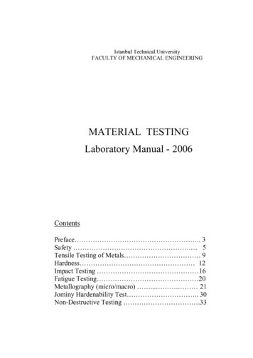
It is important to come prepared to lab. This includes the class text, the lab exercise for that day, classnotebook, calculator, and hand tools. The tools include an electronic breadboard, test leads, wirestrippers,and needle nose pliers or hemostats. A small pencil soldering iron may also be useful. A basic DMM(digital multimeter) rounds out the list.A typical breadboard or protoboard is shown below:This particular unit features two main wiring sections with a common strip section down the center.Boards can be larger or smaller than this and may or may not have the mounting plate as shown. Theconnections are spaced 0.1 inch apart which is the standard spacing for many semiconductor chips. Theseare clustered in groups of five common terminals to allow multiple connections. The exception is thecommon strip which may have dozens of connection points. These are called buses and are designed forpower and ground connections. Interconnections are normally made using small diameter solid hookupwire, usually AWG 22 or 24. Larger gauges may damage the board while smaller gauges do not alwaysmake good connections and are easy to break.In the picture below, the color highlighted sections indicate common connection points. Note the longblue section which is a bus. This unit has four discrete buses available. When building circuits on abreadboard, it is important to keep the interconnecting wires short and the layout as neat as possible. Thiswill aid both circuit functioning and ease of troubleshooting.Laboratory Manual for Semiconductor Devices: Theory and Application9
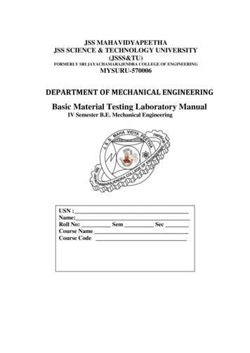
Component IdentificationIn this lab, many different electronic components are used including passive devices such as resistors andcapacitors as well as semiconductors such as diodes and transistors, and finally, integrated circuits. Thesedevices are available in many different case styles. Two broad classifications are through-hole and surfacemount. As circuits will be built on protoboards, through-hole components are of particular interest here.Surface mount devices are generally smaller and use thin flat tabs or stubs in place of ordinary wire leads.In production they are soldered directly to the surface of the printed circuit board without the use of holes.Resistors and PotentiometersResistors are perhaps the single most common component. They are classified as passive devices (versusactive devices AKA semiconductors). Resistors have two leads and are not directional so they cannot beinserted backwards. Leads are usually axial (i.e., emanating from opposite ends). The physical size of aresistor indicates its power handling capacity, not its resistance. The general purpose lab resistor isusually a carbon film type, ¼ watt dissipation. Resistance values are shown via a color coded series ofbands for most types, although high precision resistors may have the value printed directly on the body.Potentiometers may be either rotary or linear travel (slider), with rotary being the most common. Mostrotary pots are ¾ turn, although precision trim pots may be 20 turns or more. Typically, the center of thethree connections is the wiper arm. Rotary pots may be designed for panel mount (for example, a volumecontrol on a stereo) or board mount (such as a calibration control). The taper of a pot indicates howresistance and position are related. Pots may have a linear taper or a specialized audio taper (log taper). Alinear taper means that a specific degree of rotation will produce the same resistance change. Rotating the10Laboratory Manual for Semiconductor Devices: Theory and Application
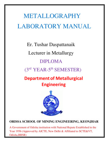
shaft half way, for example, results in a 50/50 split of the resistance. In contrast, an audio taper pot wouldshow a 10/90 split. Pots are also available in multi-gang, that is, several pots controlled by one commonshaft.Figure 1, Resistors and PotentiometersCapacitorsCapacitors are also classified as passives and can be though of as very short term energy storage devices.Capacitors are dual lead but may have either axial or radial (radiating from one end) leads. Unlikeresistors, the physical size of a capacitor offers a clue as to its capacitance and voltage rating. All otherfactors being equal the greater the capacitance or voltage rating, the larger the capacitor. Most smallercapacitors (below 1 µF) are not polarized and can be inserted into a circuit either way. The more populardielectrics for this range include the ceramics (usually disk or coin shaped) and poly film types (polyester,polypropylene, etc.) which are usually block shaped. Teardrop shaped tantalum capacitors are usedcommonly for power supply bypass. They are polarized and must be inserted in the circuit in the specifieddirection. Larger capacitance values (over 1 µF) are often realized via aluminum electrolytics. These areLaboratory Manual for Semiconductor Devices: Theory and Application11
also polarized. Failure to insert these in the proper direction may result in unpredictable results, includingthe capacitor exploding. While they do not perform as well as film types in terms of leakage, accuracy,etc., they are offer high volumetric efficiency (i.e., small physical size given the capacitance). Very largecaps may have screw terminals in place of wire leads. In years past, color coding was common but thishas generally been replaced with values printed directly on the body of the capacitor. Sometimes anumeric code is used such as “102”. This is read as 10 followed by 2 zeroes, with the result in picofarads,or 1000 pF (1 nF) in this case. Finally, because capacitors are charge storage devices, they may present ashock hazard from stored charge after they are removed from a circuit. This charge may be bled off with alow value resistance placed across the leads.Figure 2, Capacitors12Laboratory Manual for Semiconductor Devices: Theory and Application
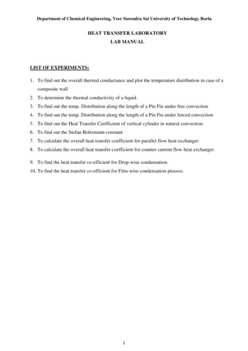
InductorsThe third and final passive device is the inductor. Also non-polarized, they normally have axial leads.Smaller values may be completely encapsulated and appear not much different from a carboncomposition resistor. Others may use some form of jacket or coating while still others show bare wire (thewire only appears bare, it is in fact covered by a thin clear insulating coating). These vary from the size ofsmall resistors to what appear to be large spools of wire.Figure 3, InductorsLaboratory Manual for Semiconductor Devices: Theory and Application13
DiodesDiodes are a two lead semiconductor. They are polarized and typically have axial leads. The two leads arereferred to as the anode and cathode. Signal diodes are around the size of ¼ watt resistors and sometimesuse a glass body. The cathode is marked by a band or stripe on the body of the diode. The cathode of anLED is usually marked by a flat spot on the plastic housing or by the shorter of the two leads. High powerdiodes are much more robust and might appear at first glance to be a short bolt or stud with leads attachedto it. Component numbers are usually stamped on the body of the device.Figure 4, Diodes14Laboratory Manual for Semiconductor Devices: Theory and Application
TransistorsThere are many types of transistors. Generally, they are three lead devices. Component model numberswill be stamped directly onto the case. Small power dissipation ( 500 mW) units will usually be seen inplastic TO-92 cases, round metal TO-5 cans or variations on the theme. Mid power devices typically useTO-220, TO-202 or the like “power tab” cases. For higher powers the oval TO-3 cases are employed. Asimilarly shaped but slightly smaller variant is the TO-66. Power devices will need to use a heat sink tokeep them cool. TO-92 cases use a flattened front face so that the three pins may be distinguished fromeach other without confusion. The round TO-5 can uses a small tab to indicate pin 1.Figure 5, TransistorsLaboratory Manual for Semiconductor Devices: Theory and Application15
Integrated CircuitsThere are a very wide variety of integrated circuits. Multi-lead versions of the TO-5 can are sometimesused but the most common through-hole package is the Dual In-Line Package, denoted as DIP or DIL. Asingle in-line package is also available for some functions. High power devices often use multi-leadversions of the popular TO-220 and TO-3 case styles. Like other semiconductors, component modelnumbers are printed directly on the package. A notch or dimple will denote which lead is pin 1 on theDIP/DIL cases.Figure 6, Integrated Circuits16Laboratory Manual for Semiconductor Devices: Theory and Application
TransformersTransformers can vary from tiny audio devices to room size devices used in power generation anddistribution. No matter the size, their job is a simple one: to isolate the source and load, to match twodifferent impedance devices or to change the voltage level. A very common application is stepping downa 120 VAC line voltage to a more modest level so that it can be rectified, filtered, and turned into a stableDC source to drive electronic circuits. Besides the voltage turns ratio, the most important characteristic isthe VA or volt-amps rating of the device. All other factors being equal, the higher the VA rating, the largerthe transformer. Transformers applicable for consumer electronics may be either chassis mount with leadsor PCB mount with through-hole pins. Transformers only operate with AC voltages.Figure 7, TransformersLaboratory Manual for Semiconductor Devices: Theory and Application17
Heat SinksHeat sinks are not a device, per se, but they are essential tools of semiconductor heat management. Theirjob is to effectively move heat from the semiconductor’s case to the surrounding air, keeping thesemiconductor cool. They range in size from small clip-ons to large extruded aluminum finned plates.Some cases, such as the body of the TO-3 or the tab of the TO-220 are electrically live. To preventpossible shorts and a live chassis, non-conductive isolating tabs and grommets are used to attach thesemiconductors to the heat sink.Figure 8, Heat Sinks18Laboratory Manual for Semiconductor Devices: Theory and Application
Laboratory Manual for Semiconductor Devices: Theory and Application19
2Resistive SensorsObjectiveThe objective of this exercise is to investigate devices that can be used to sense environmental factorssuch as light and temperature. These are important if circuitry is to react to surrounding conditions, forexample, controlling fan speed that is proportional to temperature or turning lights on or off depending onexisting light levels. Two such devices are the light dependent resistor or LDR, and the thermistor ortemperature dependent resistor. They can be thought of as resistors whose values depend on either thesurrounding light levels or the temperature.Theory OverviewOne typical LDR is the CdS (Cadmium Sulfide) cell. The resistance of the CdS cell is inverselyproportional to light levels. In darkness, it may exhibit a resistance of tens or even hundreds of kilo ohms.Under high brightness, the resistance may be as little as a few hundred ohms. Thermistors come in twotypes: PTC or Positive Temperature Coefficient whose resistive value increases with temperature, andNTC or Negative Temperature Coefficient whose resistance decreases with increasing temperature. Incontrast, ordinary resistors are designed to be immune to temperature change as much as possible.One way of using these devices is by placing them in a voltage divider. The resulting voltage will reflectthe light levels or temperature. Depending on the position of the device, the voltage can be made to eitherincrease or decrease as the environmental factor increases. For example, the voltage could rise astemperature rises but it could also be designed to have the voltage decrease as temperature rises. Bothfunctions have their uses. Finally, it is worth noting that these devices do not necessarily respondimmediately to environmental changes. For example, a thermistor might be used to sense air temperature.If the air temperature were to suddenly rise, there would be some time lag in the response of thethermistor. This is due to the fact that the thermistor itself has mass and requires some time to either heatup or cool down.Equipment(1) Adjustable DC power supplymodel: srn:(1) DMMmodel: srn:(1) Non-diffuse light source (pen light)(1) Heat source (diffused light duty heat gun or blow dryer)(1) Nominal 1 k Ω – 10 k Ω CdS cell (GL5528)(1) 10 k Ω @ 25 C NTC thermistor (Vishay NTCLE100E3)(1) 10 k Ω resistor ¼ wattactual:20Laboratory Manual for Semiconductor Devices: Theory and Application
CdS cell datasheet: aging/SEN-09088.pdfThermistor datasheet: aticsFigure 1Figure 2ProcedureLDR1. Use the DMM to measure the resistance of the LDR. Do this away from any windows and do notblock ambient room lighting from hitting the device. Record the resistance value in Table 1 under“Normal”.2. Place a finger over the LDR to block all light, making sure that the leads are not also touched. Recordthe resulting resistance value under “Dark”.3. Shine the pen light directly onto the LDR at a distance of about 25 centimeters. Record the resultunder “Bright”.4. Construct the circuit of Figure 1 using E 10 volts and R 10 k Ω. Using the voltage divider rule,determine the expected value for the voltage across R under normal lighting and then measure thevoltage. Record these values in Table 2.Laboratory Manual for Semiconductor Devices: Theory and Application21
5. Repeat step 4 for the Dark and Bright conditions.6. Finally, slowly move the pen light toward and away from the LDR. Note what happens to the voltage,recording the maximum and minimum voltages obtained in Table 3.Thermistor7. Use the DMM to measure the resistance of the LDR at room temperature and record the result in Table4. Do not handle the device excessively as body heat may affect it.8. Build the circuit of Figure 2 using E 10 volts and R 10 kΩ. Measure the voltage across thethermistor and record it in Table 5 under “Room Temp”.9. Monitor the thermistor voltage while applying heat. Caution: If you are using a standard heat gun,place it on a low setting, use a diffuser or keep the gun at least a half meter away to avoid possiblydamaging connecting wires or the protoboard. After 30 to 60 seconds, record the thermistor voltage inTable 5. Turn off the heat source and note how long it takes the thermistor circuit to recover back tothe original reading.Data TablesVariationResistanceNormalDarkBrightTable 1VariationVR TheoryVR Experiment% DeviationNormalDarkBrightTable 222Laboratory Manual for Semiconductor Devices: Theory and Application
VariationVRMaximumMinimumTable 3R at roomtemperatureTable 4VariationVthermistorRoom TempHotTable 5Questions1. If the LDR and resistor positions had been swapped, how would the values of Table 2 change?2. Would the voltages measured in Table 2 change appreciably if R had been 1 kΩ instead of 10 kΩ?3. If the positions of the thermistor and resistor in Figure 2 had been swapped, how would the Table 5values change?4. If 20 volt power sources had been used, how would the values of Tables 2 and 5 change, if at all?Laboratory Manual for Semiconductor Devices: Theory and Application23
3Diode CurvesObjectiveThe objective of this exercise is to examine the operation of the basic switching diode and to plot itscharacteristic curve. Basic DC circuit operation will also be examined.Theory OverviewThe basic diode is an asymmetric non-linear device. That is, its current-voltage characteristic is not astraight line and it is sensitive to the polarity of an applied voltage or current. When placed in forwardbias (i.e. positive polarity from anode to cathode), the diode will behave much like a shorted switch andallow current flow. When reversed biased the diode will behave much like an open switch, allowing littlecurrent flow. Unlike a switch, a silicon diode will exhibit an approximate 0.7 volt drop when forwardbiased. The precise voltage value will depend on the semiconductor material used. This volt drop issometimes referred to as the knee voltage as the resulting I-V curve looks something like a bent knee.The effective instantaneous resistance of the diode above the turn-on threshold is very small, perhaps afew ohms or less, and is often ignored. Analysis of diode circuits typically proceeds by determining if thediode is forward or reversed biased, substituting the appropriate approximation for the device, and thensolving for desired circuit parameters using typical analysis techniques. For example, when forwardbiased, a silicon diode can be thought of as a fixed 0.7 volt drop, and then KVL and KCL can be applied asneeded. The polarity of the device is typically denoted by a band placed closest to the cathode.Equipment(1) Adjustable DC power supply(1) DMM(2) Signal diodes (1N4148, 1N914)(1) 1 k Ω resistor ¼ watt(1) 10 k Ω resistor ¼ watt(1) 4.7 k Ω resistor ¼ wattmodel: srn:model: srn:actual:actual:actual:1N4148/1N914 Datasheet: 4Laboratory Manual for Semiconductor Devices: Theory and Application
SchematicsFigure 1Figure 2Figure 3ProcedureForward Curve1. Consider the circuit of Figure 1 using R 1 kΩ. For any positive value of E, the diode should beforward biased. Once E exceeds the knee voltage, all of E (minus approximately 0.7 volts) dropsacross R. Thus, as E increases, so does the diode current.2. Build the circuit of Figure 1 using R 1 kΩ. Set E to 0 volts and measure both the diode's voltageand current and record the results in Table 1. Remember, voltage is measured across a device(parallel) while current is measured through it (series). Repeat this process for the remaining sourcevoltages listed.3. From the data collected in Table 1, plot the current versus voltage characteristic of the forward biaseddiode. Make sure VD is the horizontal axis with ID on the vertical.Reverse Curve4. Consider the circuit of Figure 2 using R 1 kΩ. For any positive value of E, the diode should bereversed biased. In this case, the diode should always behave like an open switch and thus no currentshould flow. If no current flows, the voltage across R should be zero, and thus the diode voltageshould be equal to the applied source voltage. Note that the diode's voltage polarity is negative withrespect to that of Figure 1.Laboratory Manual for Semiconductor Devices: Theory and Application25
5. Build the circuit of Figure 2 using R 1 kΩ. Set E to 0 volts and measure both the diode's voltageand current and record the results in Table 2. Repeat this process for the remaining source voltageslisted.6. From the data collected in Table 2, plot the current versus voltage characteristic of the reverse biaseddiode. Make sure VD is the horizontal axis with ID on the vertical.Practical Analysis7. Consider the circuit of Figure 3 using E 12 volts, R1 10 kΩ and R2 4.7 kΩ. Analyze the circuitusing the ideal 0.7 volt forward drop approximation and determine the voltages across the tworesistors. Record the results in the first two columns of the first row (Variation 1) of Table 3.8. Build the circuit of Figure 3 using E 12 volts, R1 10 kΩ and R2 4.7 kΩ. Measure the voltagesacross the two resistors. Record the results in columns three and four of the first row (Variation 1) ofTable 3. Also compute and record the percent deviations in columns four and five.9. Reverse the direction of D1 and repeat steps 7 and 8 as Variation 2 in Table 3.10. Return D1 to the original orientation and reverse the direction of D2. Repeat steps 7 and 8 asVariation 3 in Table 3.11. Reverse the direction of both D1 and D2, and repeat steps 7 and 8 as Variation 4 in Table 3.Computer Simulation12. Repeat steps 7 through 11 using a simulator, recording the results in Table 4.26Laboratory Manual for Semiconductor Devices: Theory and Application
Data TablesE (volts)VDID000.51246810Table 1E (volts)VDID01251015Table 2VariationVR1 TheoryVR2 TheoryVR1 ExpVR2 Exp% Dev VR1% Dev VR21234Table 3Laboratory Manual for Semiconductor Devices: Theory and Application27
VariationVR1 SimVR2 Sim1234Table 4Questions1. Is 0.7 volts a reasonable approximation for a forward bias potential? Is an open circuit a reasonableapproximation for a reverse biased diode? Support your arguments with experimental data.2. The “average” resistance of a forward biased diode can be computed by simply dividing the diode'svoltage by its current. Using Table 1, determine the smallest average diode resistance (show work).3. The instantaneous resistance (also known as AC resistance) of a diode may be approximated by takingthe differences between adjacent current-voltage readings. That is, r diode ΔVdio
Programming with Python and Multisim , Operational Amplifiers & Linear Integrated Circuits, Embedded Controllers Using C and Arduino, and Science of Sound. OER texts for DC and AC Electrical Circuit Analysis, Embedded Controllers, and Operational Amplifiers &