Transcription
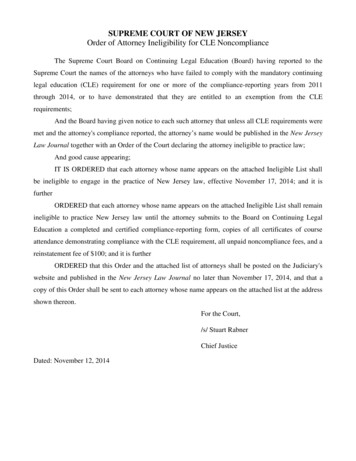
MOTOROLA Freescale Semiconductor, Inc.Order this document by:DSP56001A/D, Rev. 1SEMICONDUCTOR TECHNICAL DATADSP56001AProduct PreviewFreescale Semiconductor, Inc.24-BIT DIGITAL SIGNAL PROCESSORThe DSP56001A is an MPU-style general purpose Digital Signal Processor (DSP) composed of anefficient 24-bit DSP core, program and data memories, various peripherals, and supportcircuitry. The DSP56000 core is fed by on-chip Program RAM, two independent data RAMs, andtwo data ROMs containing sine, A-law, and µ-law tables. The DSP56001A contains a SerialCommunication Interface (SCI), a Synchronous Serial Interface (SSI), and a parallel Host Interface(HI). This combination of features, illustrated in Figure 1, makes the DSP56001A a cost-effective,high-performance solution for high-precision general purpose digital signal processing. TheDSP56001A is intended as a replacement for the DSP56001. The DSP56002 should be considered fornew designs.6315Sync.Serial(SSI)or I/OSerialComm.(SCI)or I/OHostInterface(HI)or I/O24-bit56000 DSPCore16-bit Bus24-bit BusProgramMemory512 24 RAM64 24 ROMX DataMemory256 24 RAM256 24 ROMY DataMemory256 24 RAM256 24 orData ALU24 24 56 56-bit MACTwo 56-bit ontrol7Program Control Unit2AA0884IRQFigure 1 DSP56001A Block Diagram 1997 MOTOROLA, INC.For More Information On This Product,Go to: www.freescale.com
Freescale Semiconductor, Inc.Freescale Semiconductor, Inc.TABLE OF CONTENTSSECTION 1SIGNAL/PIN DESCRIPTIONS . . . . . . . . . . . . . . . . . . . . . . . . . . . 1-1SECTION 2SPECIFICATIONS . . . . . . . . . . . . . . . . . . . . . . . . . . . . . . . . . . . . 2-1SECTION 3PACKAGING . . . . . . . . . . . . . . . . . . . . . . . . . . . . . . . . . . . . . . . . 3-1SECTION 4DESIGN CONSIDERATIONS (INCLUDES NOTESFOR DSP56001 TO DSP56001A DESIGN CONVERSION) . . . . 4-1SECTION 5ORDERING INFORMATION . . . . . . . . . . . . . . . . . . . . . . . . . . . . 5-1SECTION AROM TABLE LISTINGS . . . . . . . . . . . . . . . . . . . . . . . . . . . . . . . . A-1FOR TECHNICAL ASSISTANCE:Telephone:1 (800) ://www.motorola-dsp.comData Sheet ConventionsThis data sheet uses the following conventions:OVERBARUsed to indicate a signal that is active when pulled low; for example, the RESETpin is active when low“asserted”Means that a high true (active high) signal is high or that a low true (active low)signal is low“deasserted”Means that a high true (active high) signal is low or that a low true (active low)signal is highExamples:Note:iiSignal/SymbolLogic StateSignal IL/VOLValues for VIL, VOL, VIH, and VOH are defined by individual product specifications.DSP56001A/D, Rev. 1For More Information On This Product,Go to: www.freescale.comMOTOROLA
Freescale Semiconductor, Inc.DSP56001ADSP56001A FeaturesDSP56001A FEATURESFreescale Semiconductor, Inc.Digital Signal Processing Core Efficient, object code compatible, 24-bit 56000 family DSP engine Up to 16.5 Million Instructions Per Second (MIPS)—60.6 ns instruction cycle at 33 MHz Up to 99 Million Operations Per Second (MOPS) at 33 MHz Executes a 1024-point complex Fast Fourier Transform (FFT) in 59,898 clocks Highly parallel instruction set with unique DSP addressing modes Two 56-bit accumulators including extension byte Parallel 24 24-bit multiply-accumulate in 1 instruction cycle (2 clock cycles) Double precision 48 48-bit multiply with 96-bit result in 6 instruction cycles 56-bit addition/subtraction in 1 instruction cycle Fractional arithmetic with support for multiprecision arithmetic Hardware support for block-floating point FFT Hardware nested DO loops Zero-overhead fast interrupts (2 instruction cycles) Four 24-bit internal data buses and three 16-bit internal address buses for maximuminformation transfer on-chipMemory On-chip modified Harvard architecture permitting simultaneous accesses to programand two data memories 512 24-bit on-chip Program RAM and 64 24-bit bootstrap ROM Two 256 24-bit on-chip data RAMs Two 256 24-bit on-chip data ROMs containing sine, A-law and µ-law tables External memory expansion with 16-bit address and 24-bit data buses Bootstrap loading from external data bus or Host InterfaceMOTOROLADSP56001A/D, Rev. 1For More Information On This Product,Go to: www.freescale.comiii
Freescale Semiconductor, Inc.DSP56001AProduct DocumentationFreescale Semiconductor, Inc.Peripheral and Support Circuits Byte-wide Host Interface (HI) with Direct Memory Access (DMA) support Synchronous Serial Interface (SSI) to communicate with codecs and synchronous serialdevices–8-, 12-, 16-, and 24-bit word sizes–Up to 32 software-selectable time slots in Network mode Serial Communication Interface (SCI) for full-duplex asynchronous communications On-chip peripheral registers memory mapped in data memory space Double-buffered peripherals Up to twenty-four General Purpose I/O (GPIO) pins Two external interrupt request pinsMiscellaneous Features Power-saving Wait and Stop modes Fully static, HCMOS design for operating frequencies from 33 MHz down to 4 MHz 88-pin Ceramic Pin Grid Array (PGA) package; 13 13 array 132-pin Plastic Quad Flat Pack (PQFP) surface-mount package; 24 24 4 mm 132-pin Ceramic Quad Flat Pack (CQFP) surface-mount package; 22 22 4 mm 5 V power supplyPRODUCT DOCUMENTATIONThe three documents listed in Table 1 are required for a complete description of the DSP56001Aand are necessary to design properly with the part. Documentation is available from one of thefollowing locations (see back cover for detailed information):iv A local Motorola distributor A Motorola semiconductor sales office A Motorola Literature Distribution Center The World Wide Web (WWW)DSP56001A/D, Rev. 1For More Information On This Product,Go to: www.freescale.comMOTOROLA
Freescale Semiconductor, Inc.DSP56001AProduct DocumentationTable 1 DSP56001A DocumentationFreescale Semiconductor, Inc.TopicDescriptionOrder NumberDSP56001User’s ManualDetailed description of the 56001 architecture, 24-bitDSP, memory, peripherals, and instruction setDSP56001UM/ADDSP56001AData SheetPin and package descriptions, and electrical and timingspecificationsDSP56001A/DRelated DocumentationTable 2 lists additional documentation relevant to the DSP56001A.Table 2 DSP56001A Related DocumentationDocument NameDescriptionOrder NumberDigital Sine-Wave SynthesisApplication Report; uses the DSP56001look-up tableAPR1/DDigital Stereo 10-band GraphicEqualizerApplication Report; includes code andcircuitry; features the DSP56001APR2/DFractional and Integer ArithmeticApplication Report; includes codeAPR3/DImplementation of Fast FourierTransformsApplication Report; comprehensive FFTalgorithms and code for DSP56001,DSP56156, and DSP96002APR4/DImplementation of PID ControllersApplication Report; PWM using the SCItimer and three phase output usingmodulo addressingAPR5/DConvolutional Encoding andViterbi Decoding with a V.32Modem Trellis ExampleApplication Report; theory and code;features the DSP56001APR6/DImplementing IIR/FIR FiltersApplication Report; comprehensiveexample using the DSP56001APR7/DPrinciples of Sigma-DeltaModulation for A-to-D ConvertersApplication Report; features theDSP56ADC16; improving resolution withhalf-band filtersAPR8/DFull-Duplex 32-kbit/s CCITTADPCM Speech CodingApplication Report; features the DSP56001APR9/DDSP56001 Interface Techniquesand ExamplesApplication Report; interfaces for pseudoStatic RAM, Dynamic RAM, ISA bus, HostInterfaceAPR11/DMOTOROLADSP56001A/D, Rev. 1For More Information On This Product,Go to: www.freescale.comv
Freescale Semiconductor, Inc.DSP56001AProduct DocumentationFreescale Semiconductor, Inc.Table 2 DSP56001A Related Documentation (Continued)Document NameDescriptionTwin CODEC Expansion Board forthe DSP56000 ADSApplication Report; circuit, code, FIR filterdesign for two voice band codecsconnecting to the SSIAPR12/DConference Bridging in the DigitalTelecommunications EnvironmentApplication Report; theory and code;features the DSP56001/002APR14/DImplementation of AdaptiveControllersApplication Report; adaptive controlusing reference models; generalizedpredictive control; includes codeAPR15/DCalculating Timing Requirementsof External SRAMApplication Report; determination ofSRAM speed for optimum performanceAPR16/DLow Cost Controller for DSP56001Application Report; circuit and code toconnect two DSP56001s to an MC68008APR402/DG.722 Audio ProcessingApplication Report; theory and code usingSB-ADPCMAPR404/DMinimal Logic DRAM InterfaceApplication Report; 1M x 480 ns DRAM, 1PAL, codeAPR405/DLogarithmic/Linear ConversionRoutinesApplication Report; µ-law and A-lawcompanding routines for PCM monocircuitsANE408/DThird Party CompendiumBrochures from companies sellinghardware and software that supportsMotorola DSPsDSP3RDPTYPAK/DUniversity Support ProgramFlyer; Motorola’s program supportingUniversities in DSP research andeducationBR382/DTechnical Training ScheduleTechnical Training ScheduleBR348AD/DAudio Course InformationAudio Course InformationBR928/DReal Time Signal ProcessingApplications with Motorola’sDSP56000 FamilyTextbook by Mohamed El-Sharkawy;398 pages. (This is a charge item.)Prentice-Hall,1990; ISBN 0-13767138-5viDSP56001A/D, Rev. 1For More Information On This Product,Go to: www.freescale.comOrder NumberMOTOROLA
Freescale Semiconductor, Inc.SECTION1SIGNAL/PIN DESCRIPTIONSFreescale Semiconductor, Inc.INTRODUCTIONDSP56001A signals are organized into twelve functional groups as summarized in Table 1-1.Table 1-1 Signal Functional Group AllocationsNumberofSignalsDetailedDescriptionPower (VCCX)5Table 1-2Ground (GNDX)7Table 1-3Clock2Table 1-4Address Bus16Table 1-524Table 1-6Bus Control7Table 1-7Interrupt and Mode Control3Table 1-815Table 1-93Table 1-106Table 1-11Functional GroupPort A1Data BusPort B2Host Interface (HI) PortSerial Communications Interface (SCI) PortPort C3Synchronous Serial Interface (SSI) PortNote:1.2.3.Port A signals define the External Memory Interface port.Port B signals are GPIO signals multiplexed on the external pins also used with the HI signals.Port C signals are GPIO signals multiplexed on the external pins also used by the SCI and SSI ports.Figure 1-1 is a diagram of DSP56001A signals by functional group.MOTOROLADSP56001A/D, Rev. 1For More Information On This Product,Go to: www.freescale.com1-1
Freescale Semiconductor, Inc.DSP56001AIntroductionDSP56001AFreescale Semiconductor, X/YBR/WTBG/BSRDWRNote:1.2.3.Power Inputs:Clock OutputInternal LogicAddress BusData BusBus ControlHISSI/SCIGrounds:ClockInternal LogicAddress BusData BusBus ControlHISSI/SCI24HostInterface(HI) ��HA2HR/WHENHREQHACKPort BGPIOPB0–PB7PB8–PB10PB11PB12PB13PB14SCI PortPort CGPIOPC0PC1PC2RXDTXDRCLKSSI PortExternalAddress BusExternalData Bus83SerialCommunicationsInterface AMODBRESETSynchronousSerial Interface(SSI) Port23SC0–SC2SCKSRDSTDPort CGPIOPC3–PC5PC6PC7PC8ExternalBusControlThe Host Interface port signals are multiplexed with the Port B GPIO signals (PB0–PB15).The SCI and SSI signals are multiplexed with the Port C GPIO signals (PC0–PC8).Power and ground lines are indicated for the 144-pin TQFP package.AA0885Figure 1-1 Signals Identified by Functional Group1-2DSP56001A/D, Rev. 1For More Information On This Product,Go to: www.freescale.comMOTOROLA
Freescale Semiconductor, Inc.DSP56001APowerPOWERTable 1-2 Power ConnectionsFreescale Semiconductor, Inc.Power NamesDescriptionVCCQ (2)Internal Logic Power—These lines supply a quiet power source to the oscillatorcircuits and the mode control and interrupt lines. Ensure that the input voltage tothis line is well-regulated and uses an extremely low impedance path to tie to theVCC power rail. Use a 0.1 µF bypass capacitor located as close as possible to the chippackage to connect between the VCCQ lines and the GNDQ lines.VCCA (3)Address Bus Power—These lines supply power to the address bus.VCCD (3)Data Bus Power—These lines supply power to the data bus.VCCCBus Control Power—This line supplies power to the bus control logic.VCCH (2)Host Interface Power—These lines supply power to the Host Interface logic.VCCSSerial Interface Power—This line supplies power to the serial interface logic (SCIand SSI).GROUNDTable 1-3 Ground ConnectionsGround NamesDescriptionGNDQ (2)Internal Logic Ground—These lines supply a quiet ground connection for theoscillator circuits and the mode control and interrupt lines. Ensure that this lineconnects through an extremely low impedance path to ground. Use a 0.1 µF bypasscapacitor located as close as possible to the chip package to connect between theVCCQ line and the GNDQ line.GNDA (2)Address Bus Ground—These lines connect system ground to the address bus.GNDD (2)Data Bus Ground—These lines connect system ground to the data bus.GNDΗ (1)Host Interface Ground—These lines supply ground connections for the HostInterface logic.MOTOROLADSP56001A/D, Rev. 1For More Information On This Product,Go to: www.freescale.com1-3
Freescale Semiconductor, Inc.DSP56001AClockCLOCKTable 1-4 Clock SignalsSignalNameEXTALFreescale Semiconductor, al Clock/Crystal Input—This input should be connected to anexternal crystal or to an external oscillator.OutputChipdrivenCrystal Output—This output connects the internal crystal oscillatoroutput to an external crystal. If an external oscillator is used, XTALshould be left unconnected.Signal DescriptionADDRESS BUSTable 1-5 Address
MOTOROLA SEMICONDUCTOR TECHNICAL DATA Order this document by: DSP56001A/D, Rev. 1 1997 MOTOROLA, INC. DSP56001A Product Preview 24-BIT DIGITAL SIGNAL PROCESSOR The DSP56001A is an MPU-style general purpose Digital Signal Processor (DSP) composed of an efficient 24-bit DSP core, program and data memories, various peripherals, and support circuitry. The