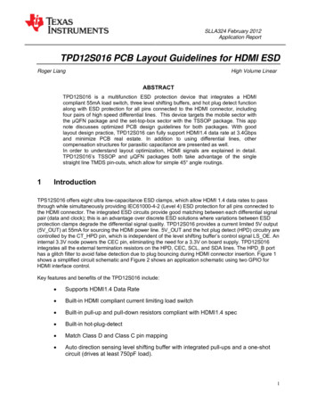
Transcription
PPCBWAY.COMPCBTECHNOLOGY
1CONTENTSWHAT IS PCB2PCB CLASSFICATION3PCBWAY.COMPCB MANUFACTURINGPROCESS
01WHAT IS PCBPCBWAY.COM
01 WHAT IS PCBA printed circuit board (PCB)mechanically supports and electricallyconnects electronic components usingconductive tracks, pads and otherfeatures etched from copper sheetslaminated onto a non-conductivesubstrate. Components are generallysoldered on the PCB.--------wikiPCBWAY.COM
02PCB CLASSFICATIONPCBWAY.COM
02 PCB CLASSFICATIONPCBWAY.COM01BY MATERIAL02BY LAYER03BY VIAS04BY SURFACE FINISH05BY HARDNEDD
02 PCB CLASSFICATION01Organic materialInorganic materialPhenolic resin, glassAluminum, Copper-fiber/epoxy,invar-copper,Polyimide, BT/Epoxy,ceramic, etc.etc.PCBWAY.COMPCBWay technologyBY MATERIAL
02 PCB CLASSFICATIONSingle layer pcb02Two layer pcbPhenolic resin, glassAluminum, Copper-fiber/epoxy,invar-copper,Polyimide, BT/Epoxy,ceramic, etc.etc.PCBWAY.COMMulti layer pcbPCBWay technologyBY LAYER
02 PCB CLASSFICATION03a. Buried via holeboardb. Blind via hole boardc. Plated through holeboardPCBWAY.COMPCBWay technologyBY VIAS
02 PCB CLASSFICATION041Hot Air Levelling5Entek/OSP2Gold finger board6Immersion gold3Carbon oil board7Immersion Tin4Gold plating board8Immersion SilverPCBWay technologyBY SURFACE FINISH
02 PCB CLASSFICATIONRigid pcb05Phenolic resin, glassAluminum, Copper-fiber/epoxy,invar-copper,Polyimide, BT/Epoxy,ceramic, etc.etc.PCBWAY.COMRigid-Flex pcbFlexible pcbPCBWay technologyBY HARDNEDD
03PCBMANUFACTURINGPROCESSPCBWAY.COM
03 PCB manufacturing processDouble sided PCB manufacturing processPCBWAY.COMPCBWAY.COM
03 PCB manufacturing processMultilayer PCB manufacturing processPCBWAY.COM
03 PCB manufacturing processPCBWAY.COM
03 PCB manufacturing processDry film/ image transferDry film is a kind of polymercompound, which can producepolymerization after irradiation ofultraviolet rays. Then will form astable substance attached to theboard surface, so as to achievethe function of blocking platingand etching.PCBWAY.COM
03 PCB manufacturing processEtching is using chemical way to removeEtchingunwanted copper from pcb. Then the circuit isappeared, usually acid is used to etch . �进行更改 �、颜色、行距等进行修改Brown OxideMaking chemical oxidation of copper surfacesto generate oxides on the surface to increaseroughness. It will improve adhesion.PCBWAY.COM
03 PCB manufacturing processAOIAutomated optical inspection (AOI) is an automated visualinspection of printed circuit board manufacture where a cameraautonomously scans the device under test for both catastrophicfailure (such as missing component) and quality defects.It is commonly used in the manufacturing process because it is anon-contact test method. This guarantees the high reliability ofMulti-CB multilayer circuit boards.PCBWAY.COM
03 PCB manufacturing processElectronic test/probe testCombine Automatic optical alignment system and the traditional flyingneedle machine together , with the help of image-processing softwareand flying-pin-only cameras, flying probe test is easier and moreaccurate.The layout is analysed according to the pcb file for short circuits andinterruptions. This is important because only the E-test detectsincorrect and broken conductors. And the detected defective circuitboard will be marked.Check https://www.youtube.com/watch?v 3wtkQx66mxkPCBWAY.COM
03 PCB manufacturing processNote:This flow is based on the most commonpcb manufacturing process . Sometimes themanufacturing process will be adjustedaccordingly to your pcb design requirement .PCBWAY.COM
PCB prototype easy wayPCBWAY.COM
inspection of printed circuit board manufacture where a camera autonomously scans the device under test for both catastrophic failure (such as missing component) and quality defects. It is commonly used in the manufacturing process because it is a non-contact test method. This guarantees the high reliabilit
