Transcription
Artix‐7 FPGAs Data Sheet:DC and AC Switching CharacteristicsDS181 (v1.27) February 10, 2022Product SpecificationIntroductionArtix -7 FPGAs are available in -3, -2, -1, -1LI, and -2Lspeed grades, with -3 having the highest performance. TheArtix-7 FPGAs predominantly operate at a 1.0V core voltage.The -1LI and -2L devices are screened for lower maximumstatic power and can operate at lower core voltages forlower dynamic power than the -1 and -2 devices,respectively. The -1LI devices operate only atVCCINT VCCBRAM 0.95V and have the same speedspecifications as the -1 speed grade. The -2L devices canoperate at either of two VCCINT voltages, 0.9V and 1.0V andare screened for lower maximum static power. Whenoperated at VCCINT 1.0V, the speed specification of a -2Ldevice is the same as the -2 speed grade. When operated atVCCINT 0.9V, the -2L static and dynamic power is reduced.Artix-7 FPGA DC and AC characteristics are specified incommercial, extended, industrial, expanded (-1Q), andmilitary (-1M) temperature ranges. Except the operatingtemperature range or unless otherwise noted, all the DCand AC electrical parameters are the same for a particularspeed grade (that is, the timing characteristics of a -1Mspeed grade military device are the same as for a -1C speedgrade commercial device). However, only selected speedgrades and/or devices are available in each temperaturerange. For example, -1M is only available in thedefense-grade Artix-7Q family and -1Q is only available inXA Artix-7 FPGAs.All supply voltage and junction temperature specificationsare representative of worst-case conditions. The parametersincluded are common to popular designs and typicalapplications.Available device and package combinations can be found in: 7 Series FPGAs Overview (DS180) Defense-Grade 7 Series FPGAs Overview (DS185) XA Artix-7 FPGAs Overview (DS197)This Artix-7 FPGA data sheet, part of an overall set ofdocumentation on the 7 series FPGAs, is available on theXilinx website at www.xilinx.com/documentation.DC CharacteristicsTable 1: Absolute Maximum Ratings(1)SymbolDescriptionMinMaxUnitsFPGA LogicVCCINTInternal supply voltage–0.51.1VVCCAUXAuxiliary supply voltage–0.52.0VVCCBRAMSupply voltage for the block RAM memories–0.51.1VVCCOOutput drivers supply voltage for HR I/O banks–0.53.6VVREFInput reference voltage–0.52.0VI/O input voltage–0.4VCCO 0.55VVIN(2)(3)(4)I/O input voltage (when VCCO 3.3V) for VREF and differential I/O standardsexcept TMDS 33(5)–0.42.625VVCCBATTKey memory battery backup supply–0.52.0VVMGTAVCCAnalog supply voltage for the GTP transmitter and receiver circuits–0.51.1VVMGTAVTTAnalog supply voltage for the GTP transmitter and receiver termination circuits–0.51.32VVMGTREFCLKReference clock absolute input voltage–0.51.32VGTP TransceiverXilinx is creating an environment where employees, customers, and partners feel welcome and included. To that end, we’reremoving noninclusive language from our products and related collateral. We’ve launched an internal initiative to removelanguage that could exclude people or reinforce historical biases, including terms embedded in our software and IPs. You may stillfind examples of non-inclusive language in our older products as we work to make these changes and align with evolving industrystandards. Follow this link for more information.DS181 (v1.27) February 10, 2022Product Specificationwww.xilinx.comSend Feedback1
Artix-7 FPGAs Data Sheet: DC and AC Switching CharacteristicsTable 1: Absolute Maximum Ratings(1) INReceiver (RXP/RXN) and Transmitter (TXP/TXN) absolute input voltageIDCIN-FLOATDC input current for receiver input pins DC coupled RX termination floating–14mAIDCIN-MGTAVTTDC input current for receiver input pins DC coupled RX termination VMGTAVTT–12mAIDCIN-GNDDC input current for receiver input pins DC coupled RX termination GND–6.5mAIDCOUT-FLOATDC output current for transmitter pins DC coupled RX termination floating–14mAIDCOUT-MGTAVTTDC output current for transmitter pins DC coupled RX termination VMGTAVTT–12mAXADCVCCADCXADC supply relative to GNDADC–0.52.0VVREFPXADC reference input relative to GNDADC–0.52.0V–65150 C– 220 C– 260 C– 125 CTemperatureStorage temperature (ambient)TSTGMaximum soldering temperature for Pb/Sn componentTSOLbodies(6)Maximum soldering temperature for Pb-free componentbodies(6)Maximum junction temperature(6)TjNotes:1.2.3.4.5.6.Stresses beyond those listed under Absolute Maximum Ratings might cause permanent damage to the device. These are stress ratings only,and functional operation of the device at these or any other conditions beyond those listed under Operating Conditions is not implied.Exposure to Absolute Maximum Ratings conditions for extended periods of time might affect device reliability.The lower absolute voltage specification always applies.For I/O operation, refer to 7 Series FPGAs SelectIO Resources User Guide (UG471).The maximum limit applies to DC signals. For maximum undershoot and overshoot AC specifications, see Table 4.See Table 9 for TMDS 33 specifications.For soldering guidelines and thermal considerations, see 7 Series FPGA Packaging and Pinout Specification (UG475).Table 2: Recommended Operating Conditions(1)(2)SymbolDescriptionMinTypMaxUnitsFor -3, -2, -2LE (1.0V), -1, -1Q, -1M devices: internal supply voltage0.951.001.05VFor -1LI (0.95V) devices: internal supply voltage0.920.950.98VFor -2LE (0.9V) devices: internal supply voltage0.870.900.93VAuxiliary supply voltage1.711.801.89VFor -3, -2, -2LE (1.0V), -2LE (0.9V), -1, -1Q, -1M devices: block RAM supplyvoltage0.951.001.05VFor -1LI (0.95V) devices: block RAM supply voltage0.920.950.98VSupply voltage for HR I/O banks1.14–3.465VFPGA LogicVCCINT(3)VCCAUXVCCBRAM(3)VCCO(4)(5)I/O input voltage–0.20–VCCO 0.20VVIN(6)I/O input voltage (when VCCO 3.3V) for VREF and differential I/O standardsexcept TMDS 33(7)–0.20–2.625VIIN(8)Maximum current through any pin in a powered or unpowered bank whenforward biasing the clamp diode.––10mAVCCBATT(9)Battery voltage1.0–1.89VGTP TransceiverVMGTAVCC(10)Analog supply voltage for the GTP transmitter and receiver circuits0.971.01.03VVMGTAVTT(10)Analog supply voltage for the GTP transmitter and receiver termination circuits1.171.21.23VXADCDS181 (v1.27) February 10, 2022Product Specificationwww.xilinx.comSend Feedback2
Artix-7 FPGAs Data Sheet: DC and AC Switching CharacteristicsTable 2: Recommended Operating Conditions(1)(2) C supply relative to GNDADC1.711.801.89VVREFPExternally supplied reference voltage1.201.251.30VJunction temperature operating range for commercial (C) temperature devices0–85 CJunction temperature operating range for extended (E) temperature devices0–100 CJunction temperature operating range for industrial (I) temperature devices–40–100 CJunction temperature operating range for expanded (Q) temperature devices–40–125 CJunction temperature operating range for military (M) temperature devices–55–125 CTemperatureTjNotes:1.2.3.4.5.6.7.8.9.10.All voltages are relative to ground.For the design of the power distribution system consult 7 Series FPGAs PCB Design and Pin Planning Guide (UG483).If VCCINT and VCCBRAM are operating at the same voltage, VCCINT and VCCBRAM should be connected to the same supply.Configuration data is retained even if VCCO drops to 0V.Includes VCCO of 1.2V, 1.35V, 1.5V, 1.8V, 2.5V, and 3.3V at 5%.The lower absolute voltage specification always applies.See Table 9 for TMDS 33 specifications.A total of 200 mA per bank should not be exceeded.VCCBATT is required only when using bitstream encryption. If battery is not used, connect VCCBATT to either ground or VCCAUX.Each voltage listed requires the filter circuit described in 7 Series FPGAs GTP Transceiver User Guide (UG482).Table 3: DC Characteristics Over Recommended Operating Data retention VCCINT voltage (below which configuration data might be lost)0.75––VVDRIData retention VCCAUX voltage (below which configuration data might be lost)1.5––VIREFVREF leakage current per pin––15µAILInput or output leakage current per pin (sample-tested)––15µACIN(2)Die input capacitance at the pad––8pFPad pull-up (when selected) @ VIN 0V, VCCO 3.3V90–330µAPad pull-up (when selected) @ VIN 0V, VCCO 2.5V68–250µAPad pull-up (when selected) @ VIN 0V, VCCO 1.8V34–220µAPad pull-up (when selected) @ VIN 0V, VCCO 1.5V23–150µAPad pull-up (when selected) @ VIN 0V, VCCO 1.2V12–120µAIRPDPad pull-down (when selected) @ VIN 3.3V68–330µAICCADCAnalog supply current, analog circuits in powered up state––25mAIBATT(3)Battery supply current––150nAThevenin equivalent resistance of programmable input termination to VCCO/2(UNTUNED SPLIT 40)284055 Thevenin equivalent resistance of programmable input termination to VCCO/2(UNTUNED SPLIT 50)355065 Thevenin equivalent resistance of programmable input termination to VCCO/2(UNTUNED SPLIT 60)446083 IRPURIN TERM(4)DS181 (v1.27) February 10, 2022Product Specificationwww.xilinx.comSend Feedback3
Artix-7 FPGAs Data Sheet: DC and AC Switching CharacteristicsTable 3: DC Characteristics Over Recommended Operating Conditions rature diode ideality factor–1.010––rTemperature diode series resistance–2– Notes:1.2.3.4.Typical values are specified at nominal voltage, 25 C.This measurement represents the die capacitance at the pad, not including the package.Maximum value specified for worst case process at 25 C.Termination resistance to a VCCO/2 level.Table 4: VIN Maximum Allowed AC Voltage Overshoot and Undershoot for HR I/O Banks(1)(2)AC Voltage OvershootVCCO 0.55% of UI @–55 C to 125 CAC Voltage Undershoot% of UI @–55 C to 125 O 0.6046.6–0.604.77VCCO 0.6521.2–0.652.10VCCO 0.709.75–0.700.94VCCO 0.754.55–0.750.43VCCO 0.802.15–0.800.20VCCO 0.851.02–0.850.09VCCO 0.900.49–0.900.04VCCO 0.950.24–0.950.02Notes:1.2.A total of 200 mA per bank should not be exceeded.The peak voltage of the overshoot or undershoot, and the duration above VCCO 0.20V or below GND – 0.20V, must not exceed the valuesin this table.DS181 (v1.27) February 10, 2022Product Specificationwww.xilinx.comSend Feedback4
Artix-7 FPGAs Data Sheet: DC and AC Switching CharacteristicsTable 5: Typical Quiescent Supply CurrentSpeed GradeSymbolICCINTQICCOQDescriptionQuiescent VCCINT supply currentQuiescent VCCO supply currentDS181 (v1.27) February 10, 2022Product ww.xilinx.comSend Feedback5
Artix-7 FPGAs Data Sheet: DC and AC Switching CharacteristicsTable 5: Typical Quiescent Supply Current (Cont’d)Speed GradeSymbolICCAUXQDescriptionQuiescent VCCAUX supply currentDS181 (v1.27) February 10, 2022Product XQ7A200TN/A73N/A7365N/AmAwww.xilinx.comSend Feedback6
Artix-7 FPGAs Data Sheet: DC and AC Switching CharacteristicsTable 5: Typical Quiescent Supply Current (Cont’d)Speed GradeSymbolDescriptionICCBRAMQ Quiescent VCCBRAM supply N/AmANotes:1.2.3.Typical values are specified at nominal voltage, 85 C junction temperature (Tj) with single-ended SelectIO resources.Typical values are for blank configured devices with no output current loads, no active input pull-up resistors, all I/O pins are 3-state andfloating.Use the Xilinx Power Estimator (XPE) spreadsheet tool (download at http://www.xilinx.com/power) to estimate static power consumption forconditions other than those specified.DS181 (v1.27) February 10, 2022Product Specificationwww.xilinx.comSend Feedback7
Artix-7 FPGAs Data Sheet: DC and AC Switching CharacteristicsPower‐On/Off Power Supply SequencingThe recommended power-on sequence is VCCINT, VCCBRAM, VCCAUX, and VCCO to achieve minimum current draw and ensurethat the I/Os are 3-stated at power-on. The recommended power-off sequence is the reverse of the power-on sequence. IfVCCINT and VCCBRAM have the same recommended voltage levels then both can be powered by the same supply and rampedsimultaneously. If VCCAUX and VCCO have the same recommended voltage levels then both can be powered by the samesupply and ramped simultaneously.For VCCO voltages of 3.3V in HR I/O banks and configuration bank 0: The voltage difference between VCCO and VCCAUX must not exceed 2.625V for longer than TVCCO2VCCAUX for eachpower-on/off cycle to maintain device reliability levels. The TVCCO2VCCAUX time can be allocated in any percentage between the power-on and power-off ramps.The recommended power-on sequence to achieve minimum current draw for the GTP transceivers is VCCINT, VMGTAVCC,VMGTAVTT OR VMGTAVCC, VCCINT, VMGTAVTT. Both VMGTAVCC and VCCINT can be ramped simultaneously. The recommendedpower-off sequence is the reverse of the power-on sequence to achieve minimum current draw.If these recommended sequences are not met, current drawn from VMGTAVTT can be higher than specifications during powerup and power-down. When VMGTAVTT is powered before VMGTAVCC and VMGTAVTT – VMGTAVCC 150 mV and VMGTAVCC 0.7V, the VMGTAVTTcurrent draw can increase by 460 mA per transceiver during VMGTAVCC ramp up. The duration of the current draw can beup to 0.3 x TMGTAVCC (ramp time from GND to 90% of VMGTAVCC). The reverse is true for power-down. When VMGTAVTT is powered before VCCINT and VMGTAVTT – VCCINT 150 mV and VCCINT 0.7V, the VMGTAVTT currentdraw can increase by 50 mA per transceiver during VCCINT ramp up. The duration of the current draw can be up to0.3 x TVCCINT (ramp time from GND to 90% of VCCINT). The reverse is true for power-down.There is no recommended sequence for supplies not shown.Table 6 shows the minimum current, in addition to ICCQ, that is required by Artix-7 devices for proper power-on andconfiguration. If the current minimums shown in Table 5 and Table 6 are met, the device powers on after all four supplieshave passed through their power-on reset threshold voltages. The FPGA must not be configured until after VCCINT is applied.Once initialized and configured, use the Xilinx Power Estimator (XPE) tools to estimate current drain on these supplies.Table 6: Power-On Current for Artix-7 itsXC7A12TICCINTQ 120ICCAUXQ 40ICCOQ 40 mA per bankICCBRAMQ 60mAXC7A15TICCINTQ 120ICCAUXQ 40ICCOQ 40 mA per bankICCBRAMQ 60mAXC7A25TICCINTQ 120ICCAUXQ 40ICCOQ 40 mA per bankICCBRAMQ 60mAXC7A35TICCINTQ 120ICCAUXQ 40ICCOQ 40 mA per bankICCBRAMQ 60mAXC7A50TICCINTQ 120ICCAUXQ 40ICCOQ 40 mA per bankICCBRAMQ 60mAXC7A75TICCINTQ 170ICCAUXQ 40ICCOQ 40 mA per bankICCBRAMQ 60mAXC7A100TICCINTQ 170ICCAUXQ 40ICCOQ 40 mA per bankICCBRAMQ 60mAXC7A200TICCINTQ 340ICCAUXQ 50ICCOQ 40 mA per bankICCBRAMQ 80mAXA7A12TICCINTQ 120ICCAUXQ 40ICCOQ 40 mA per bankICCBRAMQ 60mAXA7A15TICCINTQ 120ICCAUXQ 40ICCOQ 40 mA per bankICCBRAMQ 60mAXA7A25TICCINTQ 120ICCAUXQ 40ICCOQ 40 mA per bankICCBRAMQ 60mAXA7A35TICCINTQ 120ICCAUXQ 40ICCOQ 40 mA per bankICCBRAMQ 60mAXA7A50TICCINTQ 120ICCAUXQ 40ICCOQ 40 mA per bankICCBRAMQ 60mAXA7A75TICCINTQ 170ICCAUXQ 40ICCOQ 40 mA per bankICCBRAMQ 60mAXA7A100TICCINTQ 170ICCAUXQ 40ICCOQ 40 mA per bankICCBRAMQ 60mAXQ7A50TICCINTQ 120ICCAUXQ 40ICCOQ 40 mA per bankICCBRAMQ 60mADS181 (v1.27) February 10, 2022Product Specificationwww.xilinx.comSend Feedback8
Artix-7 FPGAs Data Sheet: DC and AC Switching CharacteristicsTable 6: Power-On Current for Artix-7 Devices NUnitsXQ7A100TICCINTQ 170ICCAUXQ 40ICCOQ 40 mA per bankICCBRAMQ 60mAXQ7A200TICCINTQ 340ICCAUXQ 50ICCOQ 40 mA per bankICCBRAMQ 80mATable 7: Power Supply Ramp amp time from GND to 90% of VCCINT0.250msTVCCORamp time from GND to 90% of VCCO0.250msTVCCAUXRamp time from GND to 90% of VCCAUX0.250msTVCCBRAMRamp time from GND to 90% of VCCBRAM0.250msTJ 125 C(1)–300TJ 100 C(1)–500TJ 85 C(1)–800TVCCO2VCCAUXAllowed time per power cycle for VCCO – VCCAUX 2.625VmsTMGTAVCCRamp time from GND to 90% of VMGTAVCC0.250msTMGTAVTTRamp time from GND to 90% of VMGTAVTT0.250msNotes:1.Based on 240,000 power cycles with nominal VCCO of 3.3V or 36,500 power cycles with worst case VCCO of 3.465V.DC Input and Output LevelsValues for VIL and VIH are recommended input voltages. Values for IOL and IOH are guaranteed over the recommendedoperating conditions at the VOL and VOH test points. Only selected standards are tested. These are chosen to ensure that allstandards meet their specifications. The selected standards are tested at a minimum VCCO with the respective VOL and VOHvoltage levels shown. Other standards are sample tested.Table 8: SelectIO DC Input and Output Levels(1)(2)I/O StandardVILVIHVOLVOHIOLIOHV, MinV, MaxV, MinV, MaxV, MaxV, MinHSTL I–0.300VREF – 0.100VREF 0.100VCCO 0.3000.400VCCO – 0.4008.00–8.00HSTL I 18–0.300VREF – 0.100VREF 0.100VCCO 0.3000.400VCCO – 0.4008.00–8.00HSTL II–0.300VREF – 0.100VREF 0.100VCCO 0.3000.400VCCO – 0.40016.00–16.00HSTL II 18–0.300VREF – 0.100VREF 0.100VCCO 0.3000.400VCCO – 0.40016.00–16.00HSUL 12–0.300VREF – 0.130VREF 0.130VCCO 0.30020% VCCO80% VCCO0.10–0.10LVCMOS12–0.30035% VCCO65% VCCOVCCO 0.3000.400VCCO – 0.400Note 3Note 3LVCMOS15–0.30035% VCCO65% VCCOVCCO 0.30025% VCCO75% VCCONote 4Note 4LVCMOS18–0.30035% VCCO65% VCCOVCCO 0.3000.450VCCO – 0.450Note 5Note 5LVCMOS25–0.3000.71.700VCCO 0.3000.400VCCO – 0.400Note 4Note 4LVCMOS33–0.3000.82.0003.4500.400VCCO – 0.400Note 4Note 4LVTTL–0.3000.82.0003.4500.4002.400Note 5Note 5MOBILE DDR–0.30020% VCCO80% VCCOVCCO 0.30010% VCCO90% VCCO0.10–0.10PCI33 3–0.40030% VCCO50% VCCOVCCO 0.50010% VCCO90% VCCO1.50–0.50SSTL135–0.300VREF – 0.090VREF 0.090VCCO 0.300 VCCO/2 – 0.150 VCCO/2 0.15013.00–13.00SSTL135 R–0.300VREF – 0.090VREF 0.090VCCO 0.300 VCCO/2 – 0.150 VCCO/2 0.1508.90–8.90SSTL15–0.300VREF – 0.100VREF 0.100VCCO 0.300 VCCO/2 – 0.175 VCCO/2 0.17513.00–13.00DS181 (v1.27) February 10, 2022Product Specificationwww.xilinx.commA, Max mA, MinSend Feedback9
Artix-7 FPGAs Data Sheet: DC and AC Switching CharacteristicsTable 8: SelectIO DC Input and Output Levels(1)(2) (Cont’d)VILI/O StandardVIHV, MaxVOLVOHIOLV, MaxV, MinIOHV, MinV, MaxV, MinmA, Max mA, MinSSTL15 R–0.300VREF – 0.100VREF 0.100VCCO 0.300 VCCO/2 – 0.175 VCCO/2 0.1758.90–8.90SSTL18 I–0.300VREF – 0.125VREF 0.125VCCO 0.300 VCCO/2 – 0.470 VCCO/2 0.4708.00–8.00SSTL18 II–0.300VREF – 0.125VREF 0.125VCCO 0.300 VCCO/2 – 0.600 VCCO/2 0.60013.40–13.40Notes:1.2.3.4.5.6.Tested according to relevant specifications.3.3V and 2.5V standards are only supported in HR I/O banks.Supported drive strengths of 4, 8, or 12 mA in HR I/O banks.Supported drive strengths of 4, 8, 12, or 16 mA in HR I/O banks.Supported drive strengths of 4, 8, 12, 16, or 24 mA in HR I/O banks.For detailed interface specific DC voltage levels, see 7 Series FPGAs SelectIO Resources User Guide (UG471).Table 9: Differential SelectIO DC Input and Output LevelsI/O StandardBLVDS 25VICM(1)V, Min V, TypVID(2)V, MaxVOCM(3)V, Min V, Typ V, MaxVOD(4)V, MinV, TypV, MaxV, Min V, Typ V, MaxNote 50.3001.2001.4250.100–––1.250–MINI LVDS 25 00.4500.600PPDS 1000.2500.400RSDS 000.3500.600TMDS 332.7002.9653.2300.1500.6751.200 VCCO–0.405 VCCO–0.300 VCCO–0.190 0.4000.6000.800Notes:1.2.3.4.5.VICM is the input common mode voltage.VID is the input differential voltage (Q – Q).VOCM is the output common mode voltage.VOD is the output differential voltage (Q – Q).VOD for BLVDS will vary significantly depending on topology and loading.Table 10: Complementary Differential SelectIO DC Input and Output LevelsI/O StandardVICM(1)VID(2)V, Min V,Typ V, Max V,Min V, MaxVOL(3)VOH(4)IOLIOHV, MaxV, MinmA, MaxmA, MinDIFF HSTL 00DIFF HSTL I .00DIFF HSTL 16.00DIFF HSTL II 16.00DIFF HSUL 120.3000.6000.8500.100–20% VCCO80% VCCO0.100–0.100DIFF MOBILE DDR 0.3000.9001.4250.100–10% VCCO90% VCCO0.100–0.100DIFF SSTL1350.3000.6751.0000.100–(VCCO/2) – 0.150(VCCO/2) 0.15013.0–13.0DIFF SSTL135 R0.3000.6751.0000.100–(VCCO/2) – 0.150(VCCO/2) 0.1508.9–8.9DIFF SSTL150.3000.7501.1250.100–(VCCO/2) – 0.175(VCCO/2) 0.17513.0–13.0DIFF SSTL15 R0.3000.7501.1250.100–(VCCO/2) – 0.175(VCCO/2) 0.1758.9–8.9DIFF SSTL18 I0.3000.9001.4250.100–(VCCO/2) – 0.470(VCCO/2) 0.4708.00–8.00DS181 (v1.27) February 10, 2022Product Specificationwww.xilinx.comSend Feedback10
Artix-7 FPGAs Data Sheet: DC and AC Switching CharacteristicsTable 10: Complementary Differential SelectIO DC Input and Output Levels (Cont’d)I/O StandardDIFF SSTL18 IIVICM(1)VID(2)V, Min V,Typ V, Max V,Min V, Max0.3000.9001.4250.100–VOL(3)VOH(4)IOLIOHV, MaxV, MinmA, MaxmA, Min(VCCO/2) – 0.600(VCCO/2) 0.60013.4–13.4Notes:1.2.3.4.VICM is the input common mode voltage.VID is the input differential voltage (Q – Q).VOL is the single-ended low-output voltage.VOH is the single-ended high-output voltage.LVDS DC Specifications (LVDS 25)Table 11: LVDS 25 DC Specifications(1)SymbolDC CCOSupply VoltageVOHOutput High Voltage for Q and QRT 100 across Q and Q signals––1.675VVOLOutput Low Voltage for Q and QRT 100 across Q and Q signals0.700––VVODIFFDifferential Output Voltage:(Q – Q), Q High(Q – Q), Q HighRT 100 across Q and Q signals247350600mVVOCMOutput Common-Mode VoltageRT 100 across Q and Q signals1.0001.2501.425VVIDIFFDifferential Input Voltage:(Q – Q), Q High(Q – Q), Q High100350600mVVICMInput Common-Mode Voltage0.3001.2001.500VNotes:1.Differential inputs for LVDS 25 can be placed in banks with VCCO levels that are different from the required level for outputs. Consult the7 Series FPGAs SelectIO Resources User Guide (UG471) for more information.DS181 (v1.27) February 10, 2022Product Specificationwww.xilinx.comSend Feedback11
Artix-7 FPGAs Data Sheet: DC and AC Switching CharacteristicsAC Switching CharacteristicsAll values represented in this data sheet are based on the speed specifications from the ISE Design Suite andVivado Design Suite as outlined in Table 12.Table 12: Artix-7 FPGA Speed Specification Version By DeviceVersion In:Typical VCCINTDeviceISE 14.7Vivado 2018.2(Table 2)N/A1.221.0VXC7A12T, XC7A15T, XC7A25T, XC7A35T, XC7A50T, XC7A75TN/A1.220.95VXC7A12T, XC7A15T, XC7A25T, XC7A35T, XC7A50T, XC7A75T, XC7A100T,XC7A200TN/A1.140.9VXC7A12T, XC7A15T, XC7A25T, XC7A35T, XC7A50T, XC7A75T1.101.221.0VXC7A100T, XC7A200T1.071.140.9VXC7A100T, XC7A200TN/A1.151.0VXA7A12T, XA7A15T, XA725T, XA7A35T, XA7A50T, XA7A75T1.071.151.0VXA7A100T1.061.111.0VXQ7A100T, XQ7A200TN/A1.111.0VXQ7A50TSwitching characteristics are specified on a per-speed-grade basis and can be designated as Advance, Preliminary, orProduction. Each designation is defined as follows:Advance Product SpecificationThese specifications are based on simulations only and are typically available soon after device design specifications arefrozen. Although speed grades with this designation are considered relatively stable and conservative, some under-reportingmight still occur.Preliminary Product SpecificationThese specifications are based on complete ES (engineering sample) silicon characterization. Devices and speed grades withthis designation are intended to give a better indication of the expected performance of production silicon. The probabilityof under-reporting delays is greatly reduced as compared to Advance data.Production Product SpecificationThese specifications are released once enough production silicon of a particular device family member has beencharacterized to provide full correlation between specifications and devices over numerous production lots. There is nounder-reporting of delays, and customers receive formal notification of any subsequent changes. Typically, the slowestspeed grades transition to Production before faster speed grades.Testing of AC Switching CharacteristicsInternal timing parameters are derived from measuring internal test patterns. All AC switching characteristics arerepresentative of worst-case supply voltage and junction temperature conditions.For more specific, more precise, and worst-case guaranteed data, use the values reported by the static timing analyzer andback-annotate to the simulation net list. Unless otherwise noted, values apply to all Artix-7 FPGAs.DS181 (v1.27) February 10, 2022Product Specificationwww.xilinx.comSend Feedback12
Artix-7 FPGAs Data Sheet: DC and AC Switching CharacteristicsSpeed Grade DesignationsSince individual family members are produced at different times, the migration from one category to another dependscompletely on the status of the fabrication process for each device. Table 13 correlates the current status of each Artix-7device on a per speed grade basis.Table 13: Artix-7 Device Speed Grade DesignationsSpeed Grade 12T-3, -2, -2LE (1.0V), -1, -1LI (0.95V), and -2LE (0.9V)XC7A15T-3, -2, -2LE (1.0V), -1, -1LI (0.95V), and -2LE (0.9V)XC7A25T-3, -2, -2LE (1.0V), -1, -1LI (0.95V), and -2LE (0.9V)XC7A35T-3, -2, -2LE (1.0V), -1, -1LI (0.95V), and -2LE (0.9V)XC7A50T-3, -2, -2LE (1.0V), -1, -1LI (0.95V), and -2LE (0.9V)XC7A75T-3, -2, -2LE (1.0V), -1, -1LI (0.95V), and -2LE (0.9V)XC7A100T-3, -2, -2LE (1.0V), -1, -1LI (0.95V), and -2LE (0.9V)XC7A200T-3, -2, -2LE (1.0V), -1, -1LI (0.95V), and -2LE (0.9V)XA7A12T-2I, -1I, and -1QXA7A15T-2I, -1I, and -1QXA7A25T-2I, -1I, and -1QXA7A35T-2I, -1I, and -1QXA7A50T-2I, -1I, and -1QXA7A75T-2I, -1I, and -1QXA7A100T-2I, -1I, and -1QXQ7A50T-2I, -1I, -1LI (0.95V), and -1MXQ7A100T-2I, -1I, -1LI (0.95V), and -1MXQ7A200T-2I, -1I, -1LI (0.95V), and -1MProduction Silicon and Software StatusIn some cases, a particular family member (and speed grade) is released to production before a speed specification isreleased with the correct label (Advance, Preliminary, Production). Any labeling discrepancies are corrected in subsequentspeed specification releases.Table 14 lists the production released Artix-7 device, speed grade, and the minimum corresponding supported speedspecification version and software revisions. The software and speed specifications listed are the minimum releases requiredfor production. All subsequent releases of software and speed specifications are valid.Table 14: Artix-7 Device Production Software and Speed Specification ReleaseSpeed GradeDevice1.0V-3XC7A12TVivado tools2018.2 do tools 2017.4 v1.20N/AN/AVivado tools2017.4 v1.20Vivado tools2018.1 v1.14N/AN/AVivado tools2014.4 v1.14Vivado tools2014.4 v1.10N/AN/AVivado tools2017.4 v1.20Vivado tools2018.1 v1.14N/AN/AVivado tools2014.4 v1.14Vivado tools2013.4 v1.08Vivado tools 2017.4 v1.20Vivado tools 2013.4 v1.11DS181 (v1.27) February 10, 2022Product Specification0.9V-1Vivado tools 2014.4 v1.14Vivado tools2018.2 v1.220.95Vwww.xilinx.comSend Feedback13
Artix-7 FPGAs Data Sheet: DC and AC Switching CharacteristicsTable 14: Artix-7 Device Production Software and Speed Specification Release (Cont’d)Speed 7A50TVivado tools 2013.4 v1.11N/AN/AVivado tools2014.4 v1.14Vivado tools2013.4 v1.08XC7A75TVivado tools 2013.3 v1.10N/AN/AVivado tools2014.4 v1.14Vivado tools2013.3 v1.07XC7A100TISE tools 14.4 or Vivado tools 2012.4 with the14.4/2012.4 device pack v1.07N/AN/AVivado tools2014.4 v1.14XC7A200TISE tools 14.4 or Vivado tools 2012.4 with the14.4/2012.4 device pack v1.07N/AN/AVivado tools2014.4 v1.14ISE tools 14.5or Vivadotools 2013.1v1.05XA7A12TN/AVivado tools2018.1 v1.15N/AVivado tools 2018.1 v1.15N/AN/AN/AXA7A15TN/AVivado tools2014.4 v1.14N/AVivado tools 2014.4 v1.14N/AN/AN/AXA7A25TN/AVivado tools2018.1 v1.15N/AVivado tools 2018.1 v1.15N/AN/AN/AXA7A35TN/AVivado tools2014.1 v1.09N/AVivado tools 2014.1 v1.09N/AN/AN/AXA7A50TN/AVivado tools2014.1 v1.09N/AVivado tools 2014.1 v1.09N/AN/AN/AXA7A75TN/AVivado tools2014.1 v1.09N/AVivado tools 2014.1 v1.09N/AN/AN/AXA7A100
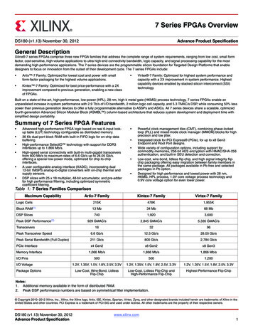
Artix -7 FPGAs are available in -3, -2, -1, -1LI, and -2L speed grades, with -3 having the highest performance. The Artix-7 FPGAs predominantly oper ate at a 1.0V core voltage. The -1LI and -2L devices are screened for lower maximum static power and can operate at lower core voltages for lower dynamic power than the -1 and -2 devices .