Transcription
2015 IEEE *Enabling FPGAs in Hyperscale Data CentersJagath Weerasinghe, Francois Abel, Christoph HagleitnerAndreas HerkersdorfIBM Research - ZurichSäumerstrasse 48803 Rüschlikon, SwitzerlandEmail: {wee,fab,hle}@zurich.ibm.comInstitute for Integrated SystemsTechnical University of Munich,Munich, GermanyEmail: herkersdorf@tum.deAbstract—FPGAs (Field Programmable Gate Arrays) are making their way into data centers (DCs) and are used to offloadand accelerate specific services, but they are not yet availableto cloud users. This puts the cloud deployment of computeintensive workloads at a disadvantage compared to on-siteinfrastructure installations, where the performance and energyefficiency of FPGAs are increasingly exploited for applicationspecific accelerators and heterogeneous computing.The cloud is housed in DCs and DCs are based on evershrinking servers. Today, we observe the emergence of hyperscaledata centers, which are based on densely packaged servers.The shrinking form factors pose serious deployment challengesfor the traditional PCIe-bus attached FPGAs. Therefore, aparadigm change is required for the CPU-FPGA and FPGAFPGA interfaces. We propose an architecture that presents theFPGA as a standalone resource connected to the DC network.This allows cloud vendors to offer an FPGA to users in asimilar way as a standard server. Since existing infrastructureas-a-service (IaaS) mechanisms are not suitable, we propose anew OpenStack (open source cloud computing software) serviceto integrate FPGAs in the cloud. This proposal is complementedby a framework that enables cloud users to combine multipleFPGAs into a programmable fabric. The proposed architectureand framework address the scalability problem that makes itdifficult to provision large numbers of FPGAs. Together, theyoffer a new solution to process large and heterogeneous data setsin the cloud.Keywords—FPGA; hyperscale data centers; cloud computing.I. I NTRODUCTIONThe use of FPGAs in application-specific processing andheterogeneous computing domains has been popular for 20years or so. However, FPGAs have only just started to beused in cloud DCs for offloading and accelerating specificapplication workloads [1]. Even though FPGAs are not yetaccessible to cloud users, they will make significant inroadsinto the cloud with more and more workloads being deployedin the cloud.Enabling FPGAs on a large scale opens new opportunities for both cloud customers and cloud vendors. From thecustomers’ perspective, FPGAs can be rented, used and released, similar to cloud infrastructure resources such as virtualmachines (VMs) and storage. For example, IaaS users canrent FPGAs for education (e.g., university classes), research(e.g., building HPC systems) and testing (e.g., evaluationprior to deployment in real environments) purposes. From thePlatform as a Service (PaaS) vendors’ perspective, FPGAs canbe used to offer acceleration as a service to the applicationdevelopers on cloud platforms. For example, PaaS vendorscan provide FPGA-accelerated application interfaces to PaaSusers. A Software as a Service (SaaS) vendor can use FPGAsto provide acceleration as a service as well as to improve userexperience. Acceleration of Bing web search service is suchan example [1].From the FPGA vendors’ perspective, the cloud expandsthe FPGA user base and also opens new paths for them tomarket their own products. For example, new products can beplaced on the cloud for users to try them out before actuallypurchasing them. In summary, the deployment of FPGAs inDCs will benefit both the users and the various cloud serviceproviders and operators.Meanwhile, the servers, which make up a cloud DC arecontinuously shrinking in terms of the form factor. This leadsto the emergence of a new class of hyperscale data centers(HSDC) based on small and dense server packaging. The smallform factor or dense packaging will enable to deploy a largenumber of FPGAs, exceeding by far the scaling capacity ofthe traditional PCIe-bus attachment.To enable large-scale deployment of FPGAs in future HSDCs, we advocate for a change of paradigm in the CPU-FPGAand FPGA-FPGA interfaces. We propose an architecture thatsets the FPGA free from the CPU and its PCIe-bus by connecting the FPGA directly to the DC network as a standaloneresource.Cloud vendors can then provision these FPGA resourcesin a similar manner to servers. However, as existing serverprovisioning mechanisms are not suitable for this purpose, wepropose a new resource provisioning service in OpenStack forintegrating such standalone FPGAs in the cloud. Once suchnetwork-attached FPGAs become available on a large scale inDCs, they can be rented by cloud users. We further proposea framework for users to interconnect multiple FPGAs into aprogrammable fabric, and for the cloud vendor to deploy sucha fabric in their infrastructure.The proposed architecture and framework enable the provisioning of a large number of FPGAs for the cloud users.Users will be able to implement customized fabrics in a costeffective, scalable and flexible manner in the cloud. Theseproposals offer new technical perspectives and solutions forprocessing large and heterogeneous data sets in the cloud.*Personal use of this material is permitted. Permission from IEEE must be obtained for all other uses, in any current or future media, includingreprinting/republishing this material for advertising or promotional purposes, creating new collective works, for resale or redistribution to servers orlists, or reuse of any copyrighted component of this work in other works. This is the accepted version of the article published by IEEE: 10.1109/UICATC-ScalCom-CBDCom-IoP.2015.199
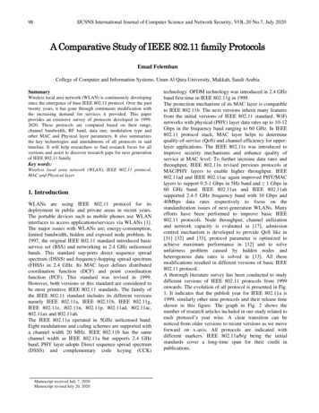
Fig. 1. Hyperscale Data Center: (a) Compute module with 24 GB DRAM(on the back). (b) 2U Rack chassis with 128 compute modules. (c) Four rackswith 8K compute modulesII. H YPERSCALE DATA C ENTERSThe scaling of modern DCs has been fuelled by the continuous shrinking of the server node infrastructure. After thetower-, rack- and blade-server form factors, a new class ofhyperscale servers (HSS) is emerging. In an HSS, the formfactor is almost exclusively optimized for the performanceper-cost metric. This is achieved by increasing the density ofCPUs per real estate and by sharing the cost of resourcessuch as networking, storage, power supply, management andcooling.At the time of writing, there are several HSSs on the market[2] [3] [4] and at the research stage [5] [6]. Among these, theHSS of DOME [5] has the objective of building the world’shighest density and most energy efficient rack unit. In thispaper, we refer to that specific type of HSS for supportingour discussion on hyperscale data centers (HSDC). Figure 1shows the packaging concept of the HSS rack chassis (19” by2U) proposed in [5]. In essence, this HSS is disaggregated intomultiple node boards, each the size of a double-height dual inline memory module (DIMM - 133mm x 55mm), which aredensely plugged into a carrier base board. A node board witha CPU and its DRAM is called a compute module (Figure 1(a)). Similarly, a node board with solid-state disks (SSD) iscalled a storage module, and a node board with a Ethernetswitch is referred to as a networking module. The use of ahomogeneous form factor is a significant contributor to theoverall cost minimization of an HSS.The base board is a passive board that provides systemmanagement, 10 GbE networking between the node boardsand multiple 40 GbE uplinks. This ultra-dense packaging iscombined with an innovative cooling system that enables theintegration of as many as 128 compute modules into a 2Uchassis (Figure 1-(b)). For a 19” rack with 16 such chassis,this amounts to 2K compute modules and 50 TB of DRAM.III. P RIOR A RTThere are a few previous attempts to enable FPGAs inthe cloud. Chen et al. [7] and Byma et al. [8] proposedframeworks to integrate virtualized FPGAs into the cloudusing the OpenStack infrastructure manager. In both cases,FPGAs are virtualized by partitioning them to multiple slots,where each slot or virtual FPGA is a partially reconfigurableregion in a physical FPGA which is attached over a PCIe-bus.In [7], a virtual FPGA model is present in each virtual machine (VM) and acts as the communication channel betweenthe applications running in the VM and the virtual FPGA. Thecommands and data communicated by the virtual FPGA modelare transferred to the virtual FPGA by the hypervisor. Thereare a few drawbacks in this framework particularly from theperspective of a cloud-based framework. First, users can notdeploy their own designs in the FPGAs, instead a limited setof applications offered by the cloud vendor has to be used.Second, if a user needs to deploy an application using severalvirtual FPGAs connected together, the data have to be copiedback and forth through the VM and hypervisor stack to feedthe next FPGA. Third, VM migration disrupts the use of thevirtual FPGA because the physical FPGA is tightly coupledto the hypervisor.In contrast to [7], the framework proposed by [8] allowsusers to deploy their own application in the FPGAs andallows those applications to be accessed over the Ethernetnetwork. In addition to that, [8] has shown that the OpenStackGlance image service can be used for managing FPGA bitstreams, which is an important factor when integrating FPGAsinto OpenStack. However, from the perspective of a clouddeployment, also this framework has a few drawbacks. First,as network, a plain Ethernet connection is offered to the virtualFPGAs which limits the flexibility of the applications that canrun on FPGAs. Second, even though multiple virtual FPGAsare enabled in a single physical FPGA, an isolation method,such as VLAN or overlay virtual network (OVN) for multitenant deployments is not supported, which is indispensablein deploying applications in the cloud.Catapult [1] is a highly customized, application-specificFPGA-based reconfigurable fabric designed to accelerate pageranking algorithms in the Bing web search engine. It is a goodexample to show the potential of FPGAs on a large scale incloud DCs. Authors claim that compared with a software-onlyapproach, Catapult can achieve 95% improvement in rankingthroughput for a fixed latency. Even though it has shown goodresults, as a system deployed in a DC it has a few drawbacks.In Catapult, similarly to the above-mentioned systems, FPGAs are PCIe-attached. But for scaling, these PCIe-attachedFPGAs are connected by a dedicated serial network, whichbreaks the homogeneity of the DC network and increases themanagement overhead. Even though maintaining a dedicatednetwork is a significant management overhead, it can be tradedoff for the good performance achieved by Catapult. However,in the case of general-purpose cloud DCs, maintaining such acustomized infrastructure is not acceptable because the FPGAsare used in diverse kinds of applications at different scalessimilarly to other DC resources such as servers and storage.All these systems deploy FPGAs tightly coupled to a severover the PCIe bus. In [1] and [7], FPGAs are accessed throughthe PCIe bus, whereas [8] uses a plain Ethernet connection.
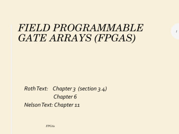
Fig. 2.Options for Attaching an FPGA to a CPUIn [1], FPGAs are chained in a dedicated network for scaling.In contrast to those systems, the focus of our proposal is toconsider the FPGA as a DC network-connected standaloneresource with compute, memory and networking capabilities.In the context of an HSDC, the FPGA resource is thereforeconsidered as a hyperscale server-class computer.IV. FPGA ATTACHMENT O PTIONSThe miniaturization of the DC servers is a game-changingrequirement that will transform the traditional way of instantiating and operating an FPGA in a DC infrastructure. Weconsider three approaches for setting up a large number ofFPGAs into an HSDC.One option is to incorporate the FPGA onto the same boardas the CPU when a tight or coherent memory coupling betweenthe two devices is desired (Figure 2-(a)). We do not expectsuch a close coupling to be generalized outside the scopeof very specific applications, such as web searching or textanalytics processing [9]. First, it breaks the homogeneity of thecompute module in an environment where server homogeneityis sought to reduce the management overhead and provideflexibility across compatible hardware platforms. Second, inlarge DCs, failed resources can be kept in place for monthsand years without being repaired or replaced, in what is oftenreferred to as a fail-in-place strategy. Therefore, an FPGA willbecome unusable and its resources wasted if its host CPUfails. Third, the footprint of the FPGA takes a significant realestate away from the compute module –the layout of a largeFPGA on a printed circuit board is somehow equivalent to thefootprint of a DDR3 memory channel, i.e. 8-16GB–, whichmay require the size of the module to be increased (e.g., bydoubling the height of the standard node board from 2U to4U). Finally, the power consumption and power dissipation ofsuch a duo may exceed the design capacity of a standard nodeboard.The second and by far the most popular option in usetoday is to implement the FPGA on a daughter-card andcommunicate with the CPU over a high-speed point-to-pointinterconnect such as the PCIe-bus (Figure 2-(b)). This pathprovides a better balance of power and physical space andis already put to use by FPGAs [1] as well as graphicsprocessing units (GPU) in current DCs. However, this typeof interface comes with the following two drawbacks whenused in a DC. First, the use of the FPGA(s) is tightly bondedto the workload of the CPU, and the fewer the PCIe-busesper CPU, the higher is the chance of under-provisioning theFPGA(s), and vice-versa. Catapult [1] uses one PCIe-attachedFPGA per CPU and solves this inelastic issue by deployinga secondary inter-FPGA network at the price of additionalcost, increased cabling and management complexity. Second,server applications are often migrated within DCs. The PCIeattached FPGA(s) affected must then be detached from thebus before being migrated to a destination where an identicalnumber and type of FPGAs must exist, thus hindering theentire migration process. Finally, despite the wide use of thisattachment model in high-performance computing, we do notbelieve that is a way forward for the deployment of FPGAsin the cloud because it confines this type of programmabletechnology to the role of coarse accelerator in the service ofa traditional CPU-centric platform.The third and preferred method for deploying FPGAs inan HSDC is to set the FPGA free from the traditional CPUFPGA attachment by hooking up the FPGA directly to theHSDC network (Figure 2-(c)). The main implication of thisscheme is that the FPGA must be turned into a standaloneappliance capable of communicating with a host CPU over thenetwork of the DC. From a practical point of view, and withrespect to the HSDC concept of section II, this is an FPGAmodule equipped with an FPGA, some optional local memoryand a network controller interface (NIC). Joining a NIC toan FPGA enables that FPGA to communicate with other DCresources, such as servers, disks, I/O and other FPGA modules.Multiple such FPGA modules can then be deployed in theHSDC independently of the number of CPUs, thus overcomingthe limitations of the two previous options.The networking layer of such an FPGA module can beimplemented with a discrete or an integrated NIC. A discreteNIC (e.g., dual 10 GbE NIC) is a sizable application-specificintegrated circuit (ASIC) typically featuring 500 pins, 400 mm2 of packaging, and 5 to 15 W of power consumption.The footprint and power consumption of such an ASIC donot favour a shared-board implementation with the FPGA (seeabove discussion on sharing board space between an FPGAand a CPU). Inserting a discrete component also adds a pointof failure in the system. Integrating the NIC into the reconfigurable fabric of the FPGA alleviates these issues. Furthermore,it provides the agility to implement a specific protocol stack ondemand, such as Virtual Extensible LAN (VxLAN), InternetProtocol version 4 (IPV4), version 6 (IPv6), TransmissionControl Protocol (TCP), User Datagram Protocol (UDP) orRemote Direct Memory Access (RDMA) over ConvergedEthernet (RoCE). Finally, the configurable implementationcan also adapt to emerging new protocols, such as GenericNetwork Virtualization Encapsulation (Geneve) and NetworkVirtualization Overlays (NVO3).In summary, we advocate a direct attachment of the FPGAto the DC network by means of an integrated NIC, and referto such a standalone FPGA as a network-attached FPGA. Thecombination of such network-attached FPGAs with emergingsoftware-defined networking (SDN) technologies brings newtechnical perspectives and market value propositions such asbuilding large and programmable fabrics of FPGAs on the
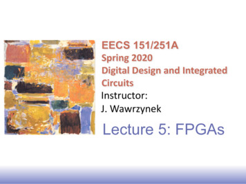
Fig. 3.High-level Architecture of the Network-attached FPGA ModuleFig. 4.Low-level Architecture of the Network-attached FPGA Modulecloud.V. S YSTEM A RCHITECTUREIn this section, we propose and describe A) the architectureof such a network-attached FPGA, B) the way it is integratedinto a cloud environment, and C) how it can be deployed andused on a large scale.A. Network-attached FPGA ArchitectureThe high-level architecture of the proposed networkattached FPGA concept is shown in Figure 3. It contains anFPGA and an optional off-chip memory. The FPGA is splitinto three main parts: i) a user logic part used for implementingcustomized applications, ii) a network service layer (NSL),which connects with the DC network, and iii) a managementlayer (ML) to run resource-management tasks.In the context of an HSDC, the FPGA concept of Figure 3is matched to the double-height DIMM form factor definedin section II and is therefore referred to as an FPGA module.The architecture of such a network-attached FPGA module isnow explained in detail with reference to Figure 4.1) User Logic (vFPGA): Multiple user applications canbe hosted on a single physical FPGA (pFPGA), somehowsimilar to multiple VMs running on the same hypervisor. Eachuser gets a partition of the entire user logic and uses it toimplement its applications. This partitioning is achieved bya feature called partial reconfiguration, a technology used todynamically reconfigure a region of the FPGA while otherregions are running untouched1 . We refer to such a partitionof user logic as a virtual FPGA (vFPGA), and it is depicted inFigure 4 as vFPGA1 and vFPGA22 . For the sake of simplicity,in this discussion we assume there is only one vFPGA in theuser logic. A vFPGA is assigned an ID (vFPGAID), an IPaddress, a MAC address and a tenant ID. The vFPGA connectsto the DC network through the NSL, and can thereforecommunicate with other vFPGAs. A vFPGA can also haveoff-chip local memory assigned to it.2) Network Service Layer (NSL): The NSL is a HW implementation of the physical, data link, network and transportlayers (L1-L4) used in a typical protocol layered architecture.These layers are mapped into the following three components:i) an Ethernet media access (MAC) controller, ii) a networkand transport stack, and iii) an application interface.a) Ethernet MAC: The Ethernet MAC implements thedata link layer of the Ethernet standard. The MAC performsfunctions such as frame delineation, cyclic redundancy check(CRC), virtual LAN extraction and collection of statistics.Normally, a MAC connects to an external physical layerdevice (PHY) whose task is to physically move the bitsover the media by means of encoding/decoding and serialization/deserialization techniques. However, because of the densepacking of an HSDC, the modules plugged on the same chassisbase board are all located within a short reach and do notrequire such a PHY to communicate with each other.Therefore, the MAC implements the networking interfaceof the FPGA module by connecting directly to the high-speedtransceivers provided in every mid- and high-end FPGA. Theseintegrated transceivers operate at line rates up to 16 Gb/s andthey commonly support the Ethernet standards 10 GBASE-KR(10 Gb/s) and 40 GBASE-KR4 (40 Gb/s) which we seek forinterconnecting our modules over a distance up to 1 meter ofcopper printed circuit board and two connectors. This PHYremoval is a key contributor in the overall power, latency, costand area savings.b) Network and Transport Stack: The network andtransport stack provides a HW implementation of L3-L4 protocols. Applications running on a cloud HW infrastructure areinherently diverse. These applications impose different communication requirements on the infrastructure. For example,one system may require a reliable, stream-based connectionsuch as TCP for inter-application communication, whereasanother system may need an unreliable, message-orientedcommunication, such as UDP. For the applications where la1 This partial reconfiguration feature is not further discussed as it exceedsthe scope of this paper2 Note that in the figure, vFPGA1 and vFPGA2 are not proportional in sizeto the NSL and the ML
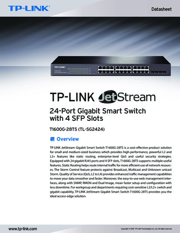
tency is critical, RoCE might be preferred. Having this networkand transport stack implemented in HW within the FPGAprovides low-latency and enables to instantiate these protocolson demand. Again, we leverage partial reconfiguration featureof the FPGA to achieve such a flexibility.Usually, a network protocol stack contains a control planeand a data plane. The control plane learns how to forwardpackets, whereas the data plane performs the actual packetforwarding based on the rules learnt by the control plane.Usually, these two planes sit close to each other in a networkstack, with the control plane distributed over the network.With the emergence of SDN, we observe that these planesare getting separated from each other. In the FPGA, it isimportant to use as few resources as possible for the NSLin order to leave more space for the user logic. To minimizethe complexity of the stack, inspired by the SDN concepts,we decouple the control plane from the HW implementationof the data plane and place it in software.The vFPGAs must be securely isolated in multi-tenantenvironments. For this isolation, it is important to use widelyused techniques such as VLANs or OVNs in order to coexistwith other infrastructure resources. Therefore, we implement atunnel endpoint (TEP) of an OVN in the network and transportstack. The TEP implemented in FPGA hardware also providesan acceleration, as software-based TEPs degrade both thenetwork and CPU performance significantly [10].The forwarding data base (FDB) sitting in the networkand transport stack contains the information on establishedconnections belonging to connection-oriented protocols andthe information on allowed packets from connection-less protocols. This information includes mac addresses, IP addresses,OVN IDs and port numbers belonging to source and destination vFPGAs. The control plane running in a centralizednetwork management software feeds this information to theFDB through the ML.c) Application Interface: The application interface comprises FIFO-based connection interfaces resembling socketbuffers in a TCP or UDP connection. The vFPGA reads fromand writes to these FIFOs to communicate with other vFPGAs.One or more FIFO interfaces can be assigned to a singlevFPGA.3) Management Layer (ML): The management layer contains a memory manager and a management stack. The memory manager enables access to memory assigned to vFPGAsand the management stack enables the vFPGAs to be remotelymanaged by a centralized management software.a) Memory Manager: The memory manager contains amemory controller and a virtualization layer. The memory controller provides the interface for accessing memory from thevFPGAs. The virtualization layer allows the physical memoryto be partitioned and shared between different vFPGAs in thesame device. This layer is configured through the managementstack according to the vFPGA memory requirements. It usesthe vFPGAID to calculate the offset when accessing thephysical memory that belongs to a particular vFPGA.b) Management Stack: The management stack runs aset of agents to enable the centralized resource-managementsoftware to manage the FPGA remotely. The agents includefunctions such as device registration, network and memoryconfiguration, FPGA reconfiguration, and a service to makethe FPGA nodes discoverable. The management stack may runon an embedded operating system in a soft core processor orpreferably in a hard core processor, like the processing systemin a Xilinx FPGA Zynq device. The network connection of theembedded OS is then shared with the HW network stack of theNSL to reduce the number of physical network connections tothe FPGA module.B. Cloud integrationCloud integration is the process of making the abovementioned vFPGAs available in the cloud so that users can rentthem. In this section, we present a framework for integratingFPGAs in the cloud that consists of a new accelerator servicefor OpenStack, a way to integrate FPGAs into OpenStack, away to provision FPGAs on the cloud, and a way for the userto rent an FPGA on the cloud.1) Accelerator Service for OpenStack: We propose a newservice for OpenStack to enable network-attached FPGAs. Inprevious research, FPGAs [8] [7] and GPUs [11] have beenintegrated into the cloud by using the Nova compute servicein OpenStack. In those cases, heterogeneous devices are PCIeattached and are usually requested as an option with virtualmachines or as a single appliance, which requires a few simpleoperations to make the device ready for use.In our deployment, in contrast, standalone FPGAs arerequested independent of a host because we want to considerthem as a new class of compute resource. Therefore, similarto Nova, Cinder and Neutron in OpenStack, which translatehigh-level service API calls into device-specific commands forcompute, storage and network resources, we propose the accelerator service shown in Figure 5, to integrate and provisionFPGAs in the cloud. In the figure, the parts in red show thenew extensions we propose for OpenStack. To setup networkconnections with the standalone FPGAs we need to carry outmanagement tasks. For that, we use an SDN stack connectedto the Neutron network service, and we call it the networkmanager. Here we explain the high-level functionality of theaccelerator-service and the network-manager components.Accelerator Service: The accelerator service comprises anAPI front end, a scheduler, a queue, a data base of FPGAresources (DB), and a worker. The API front end receives theaccelerator service calls from the users through the OpenStackdashboard or through a command line interface, and dispatchesthem to the relevant components in the accelerator service.The DB contains the information on pFPGA resources. Thescheduler matches the user-requested vFPGA to the user logicof a pFPGA by searching the information in the DB, andforwards the result to the worker. The worker executes fourmain tasks: i) registration of FPGA nodes in the DB; ii)retrieving vFPGA bit streams from the Swift object store; iii)forwarding service calls to FPGA plug-ins, and iv) forwarding
Fig. 5.OpenStack Architecture with Network-attached FPGAsnetwork management tasks to the network manager throughthe Neutron service. The queue is just there to pass servicecalls between the API front end, the scheduler and the worker.The FPGA plug-in translates the generic service calls receivedfrom the worker into device-specific commands and forwardsthem to the relevant FPGA devices. We foresee the need forone specific plug-in per FPGA vendor to be hooked to theworker. Other heterogeneous devices like GPUs and DSPs willbe hooked to the worker in a similar manner.Network Manager: The network manager is connected tothe OpenStack Neutron service through a plug-in. The networkmanager has an API front end, a set of applications, a networktopology discovery service, a virtualization layer, and an SDNcontroller. The API front end receives network service callsfrom the accelerator-worker through the Neutron and exposesapplications running in the network manager. These applications include connection management, security and servicelevel agreements (shown in red in the network manager inFigure 5). The virtualization layer provides a simplified viewof the overall DC network, including FPGA devices, to theabove applications. The SDN controller configures both theFPGAs and network switches according to the commandsreceived by the applications through the virtualization layer.2) Integrating FPGAs into OpenStack: In this sub section,the process of integrating FPGAs into OpenStack is outlined.The IaaS vendor executes this process as explained below.When the IaaS vendor powers up an FPGA module, theML of the FPGA starts up with a pre-configured IP address.This IP address is called the management IP. The acceleratorservice and the network manager use this management IP tocommunicate with the ML for executing management tasks.Second, the network-attached FPGA module is registered inthe accelerator-DB in the OpenStack accelerator service. Thisis achieved by triggering the registration process after enteringthe management IP into the accelerator service. Then theaccelerator service acquires the FPGA module informationautomatically from the ML over the network and stores themin the FPGA resource pool in the accelerator-DB. Third, afew special files 3 needed for vFPGA bitstream generation areuploaded to the OpenStack Swift object store.3) Provisioning an FPGA on the Cloud: From the IaaSvendors’ perspective, let’s now look at the process of provisioning a single vFPGA. When a request for renting avFPGA arrives, the accelerator-scheduler searches the FPGApool to find a user logic resource that matches the vFPGArequest. Once matched, the tenant ID and an IP address areconfigured for the vFPGA in the associated pFPGA. After that,the vFPGA is offered to the user with a few special files whichare used to generate a bitstream for user applicatio
Enabling FPGAs on a large scale opens new opportuni-ties for both cloud customers and cloud vendors. From the customers' perspective, FPGAs can be rented, used and re-leased, similar to cloud infrastructure resources such as virtual machines (VMs) and storage. For example, IaaS users can rent FPGAs for education (e.g., university classes .