Transcription
FPGAs 1CMPE691/491: Advanced FPGADesign
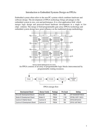
FPGAs Large array of configurable logic blocks (CLB)connected via programmable interconnects
Features and Specifications of FPGAs
Basic Programmable Devices
Features and Specifications of FPGAs
Features and Specifications of FPGAs
Features and Specifications of FPGAs
Generic Xilinx FPGA Architecture
Features and Specifications of FPGAs
Virtex FPGA family name
FPGA vs ASIC
Standard cell based ICvs. Custom design IC Standard cell based IC: Design using standard cellsStandard cells come from library providerMany different choices for cell size, delay,leakage powerMany EDA tools to automate this flowShorter design timeCustom design IC: Design all by yourselfHigher performance
Standard cell based VLSIdesign flow Front end System specification and architectureHDL coding & behavioral simulationSynthesis & gate level simulationBack end Placement and routingDRC (Design Rule Check), LVS (Layout vsSchematic)dynamic simulation and static analysis
Simple diagram of the front-enddesign flowSystemSpecificationRTLCodingEx: c !a & babSynthesisGate level codeINV (.in (a),.out (a inv));AND (.in1 (a inv), .in2 (b), .out (c));C
Simple diagram of the back-enddesign flowDRC Design rulecheckFinal layoutgate level Verilogfrom synthesisPlace&Route(go for fabrication)Gate level VerilogLVSTiming informationGate level dynamic and/or static analysisLayout vs.schematic
Flow of placement and routing Floorplan (place macros, do power planning)Placement and in-place optimizationClock tree generationRouting
Import needed files Gate level verilog (.v) Geometry information (.lef) Timing information (.lib)INV (.in (a), .out (a inv));AND (.in1 (a inv), .in2 (b), .out (c));INV: 1um width AND: 2 um widthINV: 1ns delay; AND: 2 ns delaybCaINVANDDelay (a- c): 1ns 2ns 3ns
Floorplan Size of chipLocation of PinsLocation of main blocksPower supply: give enough power for each gatePower supply (1.8V)Gate 11.75vcurrent1.7v(need another power)1.65vVDD (Metal)Gate 2Gate 3Gate 4VSSVoltage drop equation: V2 V1 – I * R
Floorplan of a single taMemOutput
Placement &in-placement optimization Placement: place the gates In-placement optimization– Why: timing information difference betweensynthesis and layout (wire delay)– How: change gate size, insert buffers– Should not change the circuit function!!
Placement of a single processor
Clock tree Main parameters: skew, delay, transition timeClock Delay xSRSETClock Skew x -yQSET SETCLRSQSQ QR RQ QCLR CLROriginal ClockSRSETQSET SETCLRSQSQ QR RQ QCLR CLRSRClock Delay ySETQSET SETCLRSQSQ QR RQ QCLR CLR
Clock tree of single processor
Routing Connect the gates using wires Two steps– Connect the global signals (power)– Connect other signals
RoutingMetal Layer Topology
Layout of a single processorArea:0.8mm x 0.8mmEstimated speed:450 MHz
Clock Tree in FPGAs Everything is preplaced and routed (there is nospace for improvement) There is no gate sizing to enhance performance
FPGA vs ASIC summary Front-end design flow is almost the same forboth Back-end design flow optimization is different– ASIC design: freedom in routing, gate sizing,power gating and clock tree optimization.– FPGA design: everything is preplaced, clock tree ispre-routed, no power gating– Designs implemented in FPGAs are slower andconsume more power than ASIC
FPGA vs DSP
DSP:FPGA vs DSP– Easy to program (usually standard C)– Very efficient for complex sequential math-intensive tasks– Fixed datapath-width. Ex: 24-bit adder, is not efficient for 5bit addition– Limited resources FPGA–––––Requires HDL language programmingEfficient for highly parallel applicationsEfficient for bit-level operationsLarge number of gates and resourcesDoes not support floating point, must construct your own.
Programming flexibility High performance– Throughput– Latency High energy efficiency Suitable for futurefabrication technologiesPerformance &Energy efficiencyCurrent trendASICManyFPGA -coreProg.DSPProgramming flexibility
Target Many-core Architecture High performance Exploit task-level parallelism indigital signal processing andmultimedia– Large number of processors perchip to support multipleapplications High energy efficiency– Voltage and frequency scalingcapability per processor34High F, VLow F, VHalt
167-processor Multi-voltage Computational Chip 164 programmable procs. Three dedicated-purpose procs. Per processor Dynamic Voltage andFrequency Scaling (DVFS)– Selects between two voltages(VDD High and VDD Low)– Programmable local oscillatorMotionEstimation16 KB SharedMemoriesFFTViterbiDecoderD. Truong, W. Cheng, T. Mohsenin, Z. Yu, A. Jacobson, G. Landge, M. Meeuwsen,C. Watnik, A. Tran, Z. Xiao, E. Work,35J. Webb, P. Mejia, B. Baas, VLSI Symp. 2008, JSSC 2009
Summary of the 167 Many-core ChipSingle TileArea0.17 mm2CMOS Tech.65 nm STMicroelectronicslow-leakageMax.frequency1.19 GHz @1.3 VPower(100%active)59 mW @1.19 GHz, 1.3 V47 mW @1.06 GHz, 1.2 V608 μW @66 MHz, 0.675 VApp. power(802.11a rx)410 μm410 μm325,0005.939 mmTransistors55 million transistors, 39.4 mm216 mW @590 MHz, 1.3 VMot.Est.MemMemMem Vit5.516 mmFFT
Design Flow
Design Flow
Features and Specifications of FPGAs
Features and Specifications of FPGAs
Features and Specifications of FPGAs
Features and Specifications of FPGAs
Features and Specifications of FPGAs
Features and Specifications of FPGAs
Features and Specifications of FPGAs
Backup
-Designs implemented in FPGAs are slower and consume more power than ASIC. FPGA vs DSP. FPGA vs DSP DSP: -Easy to program (usually standard C) -Very efficient for complex sequential math-intensive tasks -Fixed datapath-width. Ex: 24-bit adder, is not efficient for 5-bit addition