Transcription
FPGAs!? Now What?Learning FPGA Designwith the XuLA BoardDave Vandenbout, Ph.D.XESS CorporationTUT001 (V1.1) Jun 19, 2014
2011–2014 XESS, Inc. XESS, the XESS logo, and other designated brands included herein are trademarks of XESS Corporation. Allother trademarks are the property of their respective owners.This document is licensed under the Attribution-ShareAlike 3.0 Unported license, available UT001 (V1.1) Jun 19, 2014www.xess.comFPGAs!? Now What?
FPGAs!? Now What?TUT001 (V1.1) June 19, 2014The following table shows the revision history for this document.DateVersionRevision06/24/20111.0Initial release of Chapters 1-4.07/10/20111.0Added Chapter 5.08/29/20111.0Added Chapter 6.03/01/20121.0Added Chapter 7.09/04/20121.0Changed “chose” to “choose” on page 29.12/30/20121.0Changed link to XSTOOLs setup file.12/30/20121.0Added note to use 32-bit Python and avoid the 64-bit version.01/24/20131.0Revised Python scripts to use the new XsTools package.02/22/20131.0Added Chapter 8.06/19/20141.1Revised to account for XuLA2 board.TUT001 (V1.1) Jun 19, 2014www.xess.comFPGAs!? Now What?
Table of ContentsTable of ContentsPreface. 3Writing Tutorials Sucks Donkeys!.3Here I Go Again.4What This Is and Is Not.5Really Important Stuff!.6C.1 “I know nothing about FPGAs. Now what?”.7What Is Programmable Logic?.7C.2 “I have no compiler. Now what?”.12The Compilation Process: From Schematic to Bitstream.12Getting and Installing Xilinx ISE WebPACK.14C.3 “I have a synthesizer. Now what?”.27The “Hello, World” of FPGAs: the LED Blinker.27Starting a Design in WebPACK.28The Actual Blinker Design (in VHDL!).33Synthesizing the Blinker (or Not).39Testing the Logic.42C.4 “I have a netlist. Now what?”.52Physical Hardware – the XuLA Board.52Assigning I/O Signals to FPGA Pins.55Doing the Implementation.58Preparing the Bitstream.60Installing the XSTOOLs Utilities.62Connecting the XuLA Board.63Downloading the Blinker Bitstream.67C.5 “Only 12 MHz! Now what?”.69Speed Envy. 69The Digital Clock Manager.69Adding a DFS to the Blinker.70Does It Work?.73But Does It Really Work?.74C.6 “No LEDs! No buttons! Now what?”.75Blinky Envy. 75Monitoring the LED Blinker from the Host PC.77Modifying the LED Blinker Project.77Changing the XuLA Firmware.84PC Software for Talking with the LED Blinker.84Putting It All Together.85Testing a Subtractor.87Two at Once!.90So What?. 94C.7 “RAMs! Now What!?”.95Inferring RAM.95Inferring Distributed RAM.95Inferring Block RAM.103Integrating RAM into the FSM.107Inferring Multi-Port RAM.108Generating RAM.112Instantiating RAM.122TUT001 (V1.1) Jun 19, 2014www.xess.comFPGAs!? Now What?
Table of ContentsC.8 “Verilog! Now What!?”.134Simulating SDRAM.134TUT001 (V1.1) Jun 19, 2014www.xess.comFPGAs!? Now What?
PrefacePrefaceThere are numerous requests in Internet forums that go something like this:"I am new to using FPGAs. What are they? How do I start? Is there a tutorialand some cheap/free tools I can use to learn more?"The short answer is “Yes”.The long answer is this book. It will briefly describe FPGAs and then show you how toapply them to your problems using a low-cost board and some free software. Mydiscussion will be oriented towards using Xilinx FPGAs, but most of what I'll say isapplicable to other brands of FPGAs.But first, a little history.Writing Tutorials Sucks Donkeys!Yeah, I mean it and I have the experience to back it up.I've written a lot of documentation over the past twenty years. It's in the nature of mybusiness. I need to write manuals and application notes for my FPGA board customers. Ineed to generate content for my web pages. I need to write documentation for myselfjust so I can remember what I've done and where I left off.But the documentation I hate writing most of all is tutorials. With a tutorial, you can'tassume your reader knows much of anything. You have to build from the ground up. Thatrequires a lot of text, figures, pictures, design examples, etc. And you have to polish andproofread it more thoroughly to make sure its meaning is clear because, if it isn't,someone is going to read it the wrong way and give you a bunch of static about it.Allow me to take you on a trip down Memory Lane and recount some of the tutorials I'vewritten:FPGA Workout - 236 pages: I wrote this book back in 1994. It showed how to buildelectronics using the Intel FLEXlogic FPGAs. (You didn't know Intel built FPGAs? Seemsthat nobody else did either - they exited the FPGA business around 1995.) I selfpublished this and had 2000 of them printed. I sold 1500, gave 300 away (one toevery EE department in the USA), and watched the last 200 get ground under abulldozer's tracks in the Wake County landfill (I just couldn't stand having them aroundanymore).The Practical Xilinx Designer Lab Book - 300 pages: I wrote this for Prentice Hall backin 1997. They were publishing a student package in cooperation with Xilinx thatincluded this book along with the Foundation FPGA design software. It was a goodproduct at the time. My book covered how to build electronics using Xilinx FPGAs. ItFPGAs!? Now What?TUT001 (V1.1) Jun 19, 2014www.xess.com3
Prefacewas a real bear working with Prentice Hall after self-publishing my first book. I createdand proofread all the text and figures, then Prentice Hall re-entered all that materialusing Framemaker and I had to proofread it all again to catch any transcription errors.(To their credit, there weren't very many. Then again, I wasn't looking that hard.)myCSoC - 213 pages: I wrote this e-book back in 2000. It discussed how to constructelectronic systems around the Triscend TE505 chip. (The TE505 combined an 8051microcontroller with an FPGA on a single chip.) I distributed this book as PDFs from mywebsite and used it as a sales tool for the myCSoC Kit . That came to an end whenTriscend went out of business around 2003 and Xilinx gobbled up their dessicatedremains. (I still have five-hundred unused TE505 chips from that venture. Anybodywant them? Anybody?)The Practical Xilinx Designer Lab Book Version 1.5 - 450 pages: It wasn't enough to dothis once; I went ahead and did a revision! And I added an extra 150 pages of materialon - can you guess? - designing electronics using FPGAs. I tried to make a deal withPrentice Hall wherein I would write the print revision for free, and they would grant methe electronic rights to distribute it on the web. This was 1999 and they just couldn'tget their heads around this, but they knew they wanted no part of it. Instead, they justpaid me 15,000 for the re-write and told me to drop all the crazy talk. After the bookwas written, they packaged it with some CDROMs which - instead of containing theXilinx software - contained test data for an anesthesiology text book! Yeesh, thecustomer support calls I got! Looking back on it, I realized that all the whipped creamin the world would never make this turd taste any better.Pragmatic Logic Design With Xilinx Foundation 2.1i - 394 pages: This was what Ioriginally wanted to do for Prentice Hall. An online book with a separate PDF for eachchapter. Plenty of room to add as much text and as many figures as were neededbecause it didn't have to fit into a fixed amount of paper. Easily edited and changed tocorrect any errors that were found. I got five chapters of this text finished. Then Xilinxreleased a version of their free WebPACK tools that targeted FPGAs (instead of justCPLDs) and the market for the not-free Foundation software vanished. So did anyincentive I had to finish this book.Introduction to WebPACK X.Y - from 78 pages up to 130 pages: I wrote this tutorial toshow how to use the free Xilinx ISE WebPACK software, which had a markedly differentuser interface than the Foundation software. I wrote a version of the tutorial forWebPACK 1.5 and then 3.1 (these only supported Xilinx CPLDs), then two re-writes for4.1 (one for CPLDs and another for FPGAs), another re-write for 5.2 (FPGAs only, thistime), two re-writes for 6.1 (one targeting the XSA-100 board, and another for theXSB-300E board), one more minor re-write for 6.3 (because of the introduction of thenew XSA-3S1000 board), another re-write for 8.1, and a final re-write for ISEWebPACK 10. Xilinx is up to ISE 13 now and, thankfully, it still operates pretty muchthe same as version 10 because I haven't had the energy to re-write the tutorial. Itstill serves as a pretty good introduction to the Xilinx software.All told, that's over two-thousand pages of tutorials. That's a lot, regardless of whetherit's mostly roses or shit. What I hated most about doing the tutorials was the boringsameness of it. Each looks like a rehash of the previous one. So I cringe when I thinkabout writing another (hence my three year hiatus from re-doing the WebPACK tutorial).Here I Go AgainBut it looks like I am writing another one. The XuLA board needs a tutorial; it's just toodifferent from any of my other boards and the people who might use it probably have noexperience with FPGAs. So they need something to help them get started. But, in order toget me started, I'm going to write this tutorial a bit differently so it won't be so boring.Here are the guidelines I set for myself:FPGAs!? Now What?TUT001 (V1.1) Jun 19, 2014www.xess.com4
PrefaceI won't re-invent the wheel. There's no reason to re-write everything about digital logicdesign just so I can introduce you to FPGAs – the web is full of good information. I'll addlinks to good stuff I find to cut my workload and to produce a better text in less time.I won't fence it in. What I really mean is: steal this book!. I'm placing the source directoryfor it on Github. You can copy it, modify it, sell it - I don't care. I want you to do this!Please take it, add your own stuff and make it better. All I ask is that you respect theterms of the Creative Commons license I applied to this work. Basically, that means don'tremove the names/affiliations of anyone else who worked on this, and provide others withthe same rights to it that you got. (But check the actual license to get the fine points.)I won't let others fence it in. I'm using FOSS like LibreOffice and Inkscape to write thisbook. That removes some barriers for anyone who wants to work on it because theywon't have to pay for the tools. And it keeps the source files in non-proprietary formats.I won't be a prisoner of perfection. I've often held onto things too long before releasingthem, trying to remove every error I can find. That's not the case with this book – you'llfind spelling and grammar errors, subject/verb disagreements, inconsistent formatting,hand-drawn figures and lots of other stuff. But this won't matter to someone who reallyneeds the material. (For those who do care about the finer points, you can tell me whaterrors you find and I'll get around to fixing them, or you can get the source and fix themfor me.)I'll use the right medium for the right message. Text and figures are great for a tutorial soyou can read along while you actually do it. Screencasts and videos are almost alwaysmore difficult to follow, especially all the diddling-about with typing text and clicking iconsthat goes on with FPGA design tools. But there is a place for these, particularly whendemonstrating the actual operation of some circuitry.What This Is and Is NotThis book discusses how to use the Xilinx ISE WebPACK software to build FPGA designsfor the XuLA FPGA board. Along the way, you'll see: How to start an FPGA project. How to target a design to a particular type of FPGA. How to describe a logic circuit using VHDL and/or schematics. How to detect and fix VHDL syntactical errors. How to synthesize a netlist from a circuit description. How to simulate a circuit. How to implement the netlist for an FPGA. How to check device utilization and timing for an FPGA. How to generate a bitstream for an FPGA. How to download a bitstream into an FPGA. How to test the programmed FPGA. How to detect and fix errors.I'll also delve into things like: How to build hierarchical designs. How to build state machines. How to build mixed-mode designs using VHDL, Verilog and schematics.FPGAs!? Now What?TUT001 (V1.1) Jun 19, 2014www.xess.com5
Preface How to use Digital Clock Managers. How to use block RAMs. How to use multipliers. How to use IP and soft cores. How to use external components like SDRAM, VGA, audio, ADC, DAC.That said, here are some of the things this book will not teach you (I may be wrong here;this book isn't even written yet, plus who knows what others may add): It will not teach you how to use VHDL. There are plenty of good VHDL textbooksalready. It will not teach you how to choose the best type of FPGA for your particulardesign. I'm oriented toward using the FPGA on the XuLA board. It will not show you every feature of the ISE software and discuss how to setevery option and property. This software already has a good help system andextensive manuals, so those should suffice.In short, this book will get you started using the XILINX ISE software for doing FPGAdesigns with the XuLA board. After you finish, you should be able to move on to moreadvanced topics.Really Important Stuff! Everything for this book is on Github! That includes all the FPGA design examples.https://github.com/xesscorp/FpgasNowWhat if you need anything related to thisbook. In a change of heart from my previous stance, I'm also making an archiveof just the design examples available there which you can get without having todownload the entire repository. All the examples discussed in this book are targeted to the XuLA-200 board.Here's what to do if you're using one of our other XuLA board models:FPGAs!? Now What?TUT001 (V1.1) Jun 19, 2014 For the XuLA-50 board, change the target FPGA in the XuLA-200 projectfrom xc3s200a-4vq100 to xc3s50a-4vq100. For the XuLA2-LX25 board, there is a copy of the corresponding XuLA200 project with the settings changed to accommodate xc6slx252ftg256 FPGA. For the XuLA2-LX9 board, change the target FPGA in the XuLA2-LX25project from xc6slx25-2ftg256 to xc6slx9-2ft256.www.xess.com6
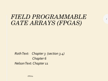
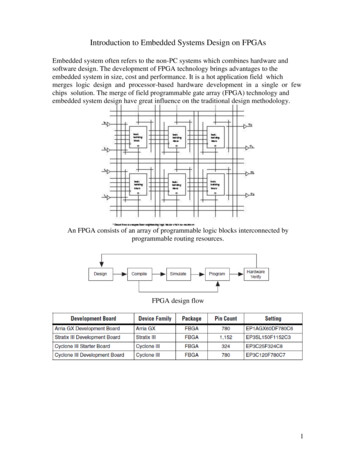
C.1 “I know nothing aboutFPGAs. Now what?”What Is Programmable Logic?In the beginning (OK, actually in the 60's) there were discrete logic chips. Systems werebuilt from lots of individual ANDs, ORs, flip-flops, etc. with a spaghetti-like maze of wiringbetween them. It was difficult to modify such a system after you built it. Jeez, after aweek or two it was difficult to remember what each of the chips was for!Spaghetti wiring (courtesy ofwww.franksworkshop.com.au).FPGAs!? Now What?TUT001 (V1.1) Jun 19, 2014www.xess.com7
“I know nothing aboutFPGAs. Now what?”Manufacturing a system like this took a lot of time because each design change requiredthat the wiring be redone which usually meant building a new printed circuit board. Thechip makers addressed this problem by placing an unconnected array of AND-OR gates ina single chip called a programmable logic device (PLD). The PLD contained an array offuses that could be blown open or left closed to connect various inputs to each AND gate.You could program a PLD with a set of Boolean sum-of-product equations to perform thelogic functions needed in your system. You could change the function of a design byremoving the PLDs, blowing a new fuse pattern into them, and then placing them backinto the circuit board. This reduced the need to change the actual wiring of the printedcircuit boards which held them.Simple PLDs could only handle up to 10–20 logic equations, so you couldn't fit a verylarge logic design into just one of them. You had to figure out how to break your largerdesigns apart and fit them into a set of PLDs. This was time-consuming and meant youhad to interconnect the PLDs with wires. The wires were a big no-no because eventuallyyou would make some design change that couldn't be handled just by reprogramming thePLDs and then you would have to build a new circuit board. The chip makers came to therescue again by building much larger programmable chips called complex programmablelogic devices (CPLDs) and field-programmable gate arrays (FPGAs). With these, you couldessentially get a complete system onto a single chip.FPGAs!? Now What?TUT001 (V1.1) Jun 19, 2014www.xess.com8
“I know nothing aboutFPGAs. Now what?”A CPLD contains a bunch of PLD blocks like the one shown above, but their inputs andoutputs are connected together by a global interconnection matrix. So a CPLD has twolevels of programmability: each PLD block can be programmed, and then theinterconnections between the PLDs can be programmed.An FPGA takes a different approach. It has a bunch of simple, configurable logic blocks(CLBs) interspersed within a switching matrix that can rearrange the interconnectionsbetween the them. Each logic block is individually programmed to perform a logic function(such as AND, OR, XOR, etc.) and then the switches are programmed to connect theblocks so that the complete logic functions are implemented.CPLD and FPGA manufacturers use a variety of methods to make the connectionsbetween logic blocks. Some make chips with fuses or anti-fuses that are programmed byFPGAs!? Now What?TUT001 (V1.1) Jun 19, 2014www.xess.com9
“I know nothing aboutFPGAs. Now what?”passing a large current through them. These types of CPLDs and FPGAs are one-timeprogrammable (OTP) because you can't rewire them internally once the fuses are blown.Other manufacturers make the connections using pass transistors that are opened orclosed by storing a charge on their gate electrodes using a high-voltage pulse. This typeof programmable device resembles an EPROM or EEPROM: you can erase it and thenplace it in a special programmer socket and reprogram it. That's fine unless you have theCPLD or FPGA soldered into a circuit board.Finally, some manufacturers use static RAM or Flash bits to control the pass transistors foreach interconnection. By loading each bit with a 1 or a 0, you can control whether theswitch is closed or opened and, therefore, whether two logic elements are connected ornot. CPLDs and FPGAs built using RAM/Flash switches can be reprogrammed withoutremoving them from the circuit board. They are often said to be in-circuitreconfigurable or in-circuit programmable. They are different, however: a Flash-basedFPGA always has its programming intact whether it is powered or not, but a RAM-basedFPGA will be erased and stop functioning if it ever loses power. Even with this drawback,most FPGAs are RAM-based because the RAMs can be built on the chip using the samemanufacturing process as for the CLBs and switches (that makes the chips cheaper toproduce). The manufacturers also provide a separate, Flash-based chip that stores theprogramming switch settings externally and loads it into the FPGA whenever power isapplied.For the rest of this book, we'll concentrate on using RAM-based FPGAs from Xilinx. I'llintroduce a little terminology because it will be important later on.Within the CLBs of an FPGA are look-up tables (LUTs) that perform the actual logicoperations. These are usually built as small RAMs that are loaded with a truth table. Forexample, an eight-bit RAM can perform a three-input AND operation if it is loaded asfollows:If the inputs for the AND gate are applied to the address pins of the RAM, then the outputof the RAM will only be 1 when location 7 111 is selected. This is exactly how a threeinput AND gate would operate. By setting the contents of the RAM in the right way, youcan perform any logic function of three binary inputs. (Modern FPGAs use LUTs with fourto six inputs.)The output of a LUT can be used directly as an input to another LUT to make morecomplicated logic functions. Or it can be stored in a flip-flop for later use (there's usuallyat least one register for each LUT).The switching matrix routes all the signals between the LUTs and registers and also to theI/O blocks (IOBs) around the perimeter of the FPGA chip. The IOBs connect selectedinternal signals of the FPGA to the outside world and contain special analog circuitry toFPGAs!? Now What?TUT001 (V1.1) Jun 19, 2014www.xess.com10
“I know nothing aboutFPGAs. Now what?”adjust the input and output voltage levels, insert small delays, and handle single-endedor differential signaling.Over time, other types of more specialized circuit blocks have found their way into FPGAs:blocks of RAM, multipliers and DSP blocks, delay-locked and phase-locked loops, gigabitserial transceivers, and even complete microprocessors. But, at least when you're startingoff, your main concern will be the LUTs and registers. These are the equivalent of theprogram and data memories in a processor: the values in the LUTs and flip-flopsdetermine how your logic circuit functions, and your design must fit into the availablenumber of LUTs and flip-flops within your target FPGA.Also, like a microprocessor, you need a way to write programs for your FPGA. That's thesubject of the next chapter.FPGAs!? Now What?TUT001 (V1.1) Jun 19, 2014www.xess.com11
C.2 “I have no compiler.Now what?”The Compilation Process: From Schematic to BitstreamAs you can imagine, figuring out which bits to set in the LUTs and the switching matrix inorder to create a logic circuit is quite a chore. Not many people would want to delve intothe details of this (probably the same ones who like to program in assembly). That's whythe FPGA manufacturers provide development software that compiles a high-leveldescription of a logic design and outputs a bitstream which sets the FPGA configurationbits appropriately.The process the development software goes through to compile a design into a bitstreamis depicted in the figure on the next page. Here's what happens:1. You enter a description of your logic circuit using a hardware descriptionlanguage (HDL) such as VHDL or Verilog. Or you can also draw your design usinga schematic editor. Or you can use a combination of the two.2. A logic synthesizer transforms the HDL into a netlist. The netlist is just adescription of the various logic gates in your design and how they areinterconnected. (A schematic is already pretty close to a netlist, so it doesn't needas much work done on it as the HDL code.)3. The implementation phase employs three different tools. A translator mergestogether one or more netlists along with any design constraints (don't worryabout those now). This is fed to a mapper that combines gates in the netlist intogroups that will fit efficiently into the LUTs of the FPGA. The gate groupings aresent to the place & route tool that assigns them to LUTs at various locations in theFPGA and then determines how to connect them together using the routingresources (wires) in the switching matrix. This part takes the most time as findinga placement that can be routed efficiently requires a lot of computation.4. A bitstream generator takes the output of the implementation phase, combines itwith a few other configuration settings, and outputs a binary bitstream. Thisbitstream (which, depending upon the size of the FPGA, can be many megabits inlength) contains the truth-tables that will be loaded into the RAM of every LUTand the connection settings for the wiring matrix that will connect them.5. At this point, a bitstream is just a bunch of 1s and 0s in a file on the computer.The downloader will transfer this file into a physical FPGA chip. In most cases, thischip is already mounted on a circuit board where it waits for the bitstream thatwill make it perform its intended function.FPGAs!? Now What?TUT001 (V1.1) Jun 19, 2014www.xess.com12
“I have no compiler. Now what?”FPGAs!? Now What?TUT001 (V1.1) Jun 19, 2014www.xess.com13
“I have no compiler. Now what?”After downloading, you can apply patterns of input signals (or test vectors) to the I/Opins of the FPGA to check the operation of your design. This is often an effective way todo testing, but sometimes it's difficult to set up a particular combination of signals andlook deeply into the internals of your design to see why it may not be performing as youintended.If that's the case, you can use a simulator to try out test examples and see how yourcircuit reacts before you actually load it into an FPGA. There are several places in thedesign flow where you can perform a simulation. If you capture the netlist before it entersthe implementation tools, you can run a logic simulation that only tests the logicaloperations of the gates in your circuit. Such simulations are good for debugging the basicfunctions of your design.As you tap the design flow at points further downstream, the netlist is augmented withmore and more information about how your design will be placed into the FPGA. Thisallows you to perform a more realistic timing simulatio
4.1 (one for CPLDs and another for FPGAs), another re-write for 5.2 (FPGAs only, this time), two re-writes for 6.1 (one targeting the XSA-100 board, and another for the XSB-300E board), one more minor re-write for 6.3 (because of the introduction of the new XSA-3S1000 board), another re-write for 8.1, and a final re-write for ISE WebPACK 10.