Transcription
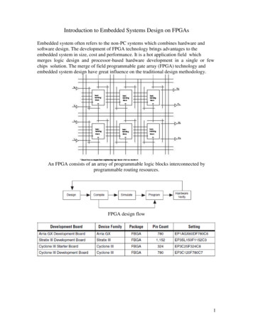
Introduction to Embedded Systems Design on FPGAsEmbedded system often refers to the non-PC systems which combines hardware andsoftware design. The development of FPGA technology brings advantages to theembedded system in size, cost and performance. It is a hot application field whichmerges logic design and processor-based hardware development in a single or fewchips solution. The merge of field programmable gate array (FPGA) technology andembedded system design have great influence on the traditional design methodology.An FPGA consists of an array of programmable logic blocks interconnected byprogrammable routing resources.FPGA design flow1
Hands-on: FPGA design and run it on a FPGA development boardImplement a simple Boolean Equation X AB CD, and illustrate the steps involved todesign, simulate, and program a FPGA using Altera’s Quartus’ II software.A. Create a new project:1) Create a new project:2) Fill a name and top-level entity for the project.Select path C:\My Documents\workshop, name your project “IntroFPGA”3) Press Next2
4)Select Cyclone II family, and choose EP2C35F672C6 which is the FPGA used onAltera’s DE2 board5) Press Next and click FinishB. Block Design File (bdf format)1) Choose New from File menu3
2) Highlight a new Block Diagram File3) Choose Save As4) Enter the file name of IntroFPGA and press Save4
5) Right click the mouse in the empty workspace6) Insert - Symbol of and2 (2 input AND logic gate)7) Assign the name “LogicGate1” to and2 gate5
7) Repeat steps of 5) and 6) and insert a symbol and2Assign the name “LogicGate2” to and28) Insert - Symbol or2 (LogicGate3) and assign the name6
9) Make wire connection and insert input/output pin to implement X AB CD. The bdfworkspace now has gates of AND and OR, and 4 input pins and 1 output pin. Thenmake circuit connections.7
10) Change input and output terminal name to A, B, C, D, and X, respectively.C. Compiling the project1) Choose Processing - Start Compilation2) Message indicated no error8
D. Create a Vector Waveform File (vwf) to simulate the design1) Choose File - New - Other Files - Vector Waveform File - OK2) Save the vector waveform file (wvf) as IntroFPGA. Check the box of Add file tocurrent project9
3) Build the simulation file (vwf) with ending time of 20µs and grid size of 1 µs10
4) View - Fit in Window11
6) Add inputs and outputs to the waveform (vwf)Right click and select Insert Node or Bus7) Click Node Finder12
6) Choose Filter: Design Entry (All Name)7) Select inputs/outputs names from Node Finder screen to the right side and click OK8) Highlight the input A, choose Edit Value Clock. Enter a period of 2µs, press Ok13
9) Highlight the input B, choose Edit Value Clock. Enter a period of 4µs, press OK10) Highlight the input C, choose Edit Value Clock. Enter a period of 8µs, press Ok11) Highlight the input D, choose Edit Value Clock. Enter a period of 16µs,press Ok12) Choose File Save as IntroFPGA.vwf fileE. Perform a simulation of the X-output1) Choose Processing Start Simulation14
2) Show the results of the simulation for the Boolean equation X AB CDF. Programming the FPGA using the Altera DE2 Programmer Board (hardwareconfiguration)1) Connect SW0, SW1, SW2, SW3 and LEDG0 to the associated pin numberInput SwitchOutput LED Bank 1Switch NumberPin NumberLED NumberPin NumberSW0 (A)PIN N25LEDG0 (X)PIN AE22SW1 (B)PIN N26SW2 (C)PIN P25SW3 (D)PIN AE142) Assign specific pin numbers in the IntroFPGA for connecting to the DE2 boardChoose Assignment - Pins from the assignment Editor screen3) Choose File - Save Project.The bdf file showing the pin assignments15
4) Choose Processing - Compilation.After the compilation is successful, press OK5) JTAP Programing and Configuring the FPGA Device.The FPGA device must beprogrammed and configured to implement the designed circuit.i) Flip the RUN/PROG switch of DE2 development into the RUN position (default)ii) Choose Tools- Programmer.16
iii) Click Hardware Setup - Select Add Hardwareiv) Choose USB-Blaster (Hardware type) press Closev) Make sure Program/Configure check box6) Download the embedded system design to Altera EP2C35F672C6. Press Start forstarting the programming process until progress 100%17
G. Test the download design (X AB CD ) to the FPGA chip by combinations of inputlevels and observation of the output respondsTruth Table for Testing the FPGA program for X AB CDA (SW0)B (SW1)C (SW2)D (SW3)0 (DOWN)0 (DOWN)0 (DOWN)0 (DOWN)0 (DOWN)0 (DOWN)0 (DOWN)1 (DOWN)0 (DOWN)0 (DOWN)1 (UP)0 (DOWN)0 (DOWN)0 (DOWN)1 (UP)1 (UP)0 (DOWN)1 (UP)0 (DOWN)0 (DOWN)0 (DOWN)1 (UP)0 (DOWN)1 (UP)0 (DOWN)1 (UP)1 (UP)0 (DOWN)0 (DOWN)1 (UP)1 (UP)1 (UP)1 (UP)0 (DOWN)0 (DOWN)0 (DOWN)1(UP)0 (DOWN)0 (DOWN)1 (UP)1 (UP)0 (DOWN)1 (UP)0 (DOWN)1 (UP)0 (DOWN)1 (UP)1 (UP)1 (UP)1 (UP)0 (DOWN)0 (DOWN)1 (UP)1 (UP)0 (DOWN)1 (UP)1 (UP)1 (UP)1 (UP)0 (DOWN)1 (UP)1 (UP)1 (UP)1 (UP)X(LED)0 (Led off)0 (Led off)0 (Led off)1 (Led on)0 (Led off)0 (Led off)0 (Led off)1 (led on)0 (Led off)0 (Led off)0 (Led off)1 (Led on)1 (Led on)1 (Led on)1 (Led on)1 (Led on)H. Your turn – PracticeFollow the steps to update your design by adding four buffers. Design and test the logicto implement the circuit shown in the figure bellow.1) Work on the design entry IntroFPGA.bdf and insert buffers to your design18
2) Insert output pins and update the names of outputs: LEDR0, LEDR1, LEDR2, andLEDR33) Save your file and Compile your design and see if any error4) Update Pin Planner and configuration to make connection between logic pins toassociated FPGA pins.5) Compile your design with FPGA device hardware6) Download the design to FPGA IC. Observe the output LEDs and inputs Switches7) Explore different led lights by your own.19
20
Introduction to Embedded Systems Design on FPGAs Embedded system often refers to the non-PC systems which combines hardware and software design. The development of FPGA technology brings advantages to the embedded system in size,