Transcription
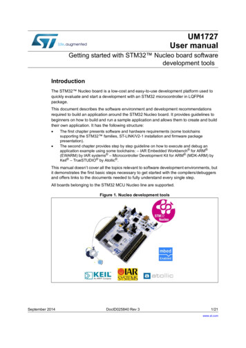
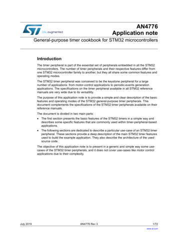
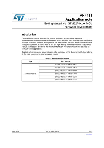
UM1956User manualSTM32 Nucleo-32 boards (MB1180)IntroductionThe STM32 Nucleo-32 boards based on the MB1180 reference board (NUCLEO-F031K6,NUCLEO-F042K6, NUCLEO-F301K8, NUCLEO-F303K8, NUCLEO-L011K4, NUCLEOL031K6, NUCLEO-L412KB, NUCLEO-L432KC) provide an affordable and flexible way forusers to try out new concepts and build prototypes with STM32 microcontrollers, choosingfrom the various combinations of performance, power consumption and features. TheArduino Nano connectivity support makes it easy to expand the functionality of theNucleo-32 open development platform with a wide choice of specialized shields. TheSTM32 Nucleo-32 boards do not require any separate probe as they integrate the STLINK/V2-1 debugger/programmer and come with the STM32 comprehensive software HALlibrary, together with various packaged software examples, as well as direct access to theArm Mbed online resources at http://mbed.org.Figure 1. STM32 Nucleo-32 boardPicture is not contractual.November 2018UM1956 Rev 51/37www.st.com1
ContentsUM1956Contents1Features . . . . . . . . . . . . . . . . . . . . . . . . . . . . . . . . . . . . . . . . . . . . . . . . . . . 62Product marking . . . . . . . . . . . . . . . . . . . . . . . . . . . . . . . . . . . . . . . . . . . . 73Ordering information . . . . . . . . . . . . . . . . . . . . . . . . . . . . . . . . . . . . . . . . 74Conventions . . . . . . . . . . . . . . . . . . . . . . . . . . . . . . . . . . . . . . . . . . . . . . . . 85Quick start . . . . . . . . . . . . . . . . . . . . . . . . . . . . . . . . . . . . . . . . . . . . . . . . . 965.1Getting started . . . . . . . . . . . . . . . . . . . . . . . . . . . . . . . . . . . . . . . . . . . . . . 95.2System requirements . . . . . . . . . . . . . . . . . . . . . . . . . . . . . . . . . . . . . . . . . 9Hardware layout and configuration . . . . . . . . . . . . . . . . . . . . . . . . . . . . 106.1STM32 Nucleo-32 board layout . . . . . . . . . . . . . . . . . . . . . . . . . . . . . . . . .116.2STM32 Nucleo-32 board mechanical drawing . . . . . . . . . . . . . . . . . . . . . 136.3Embedded ST-LINK/V2-1 . . . . . . . . . . . . . . . . . . . . . . . . . . . . . . . . . . . . . 146.46.3.1Drivers. . . . . . . . . . . . . . . . . . . . . . . . . . . . . . . . . . . . . . . . . . . . . . . . . 146.3.2ST-LINK/V2-1 firmware upgrade . . . . . . . . . . . . . . . . . . . . . . . . . . . . . . 15Power supply and power selection . . . . . . . . . . . . . . . . . . . . . . . . . . . . . . 166.4.1Power supply input from USB connector . . . . . . . . . . . . . . . . . . . . . . . . 166.4.2External power supply inputs . . . . . . . . . . . . . . . . . . . . . . . . . . . . . . . . . 17VIN or 5 V power supply. . . . . . . . . . . . . . . . . . . . . . . . . . . . . . . . . . . . . . . . . . .17 3V3 power supply . . . . . . . . . . . . . . . . . . . . . . . . . . . . . . . . . . . . . . . . . . . . . . . .186.4.372/37External power supply output . . . . . . . . . . . . . . . . . . . . . . . . . . . . . . . . 186.5LEDs . . . . . . . . . . . . . . . . . . . . . . . . . . . . . . . . . . . . . . . . . . . . . . . . . . . . 186.6Push-button . . . . . . . . . . . . . . . . . . . . . . . . . . . . . . . . . . . . . . . . . . . . . . . 186.7JP1 (IDD) . . . . . . . . . . . . . . . . . . . . . . . . . . . . . . . . . . . . . . . . . . . . . . . . . 196.8OSC clock . . . . . . . . . . . . . . . . . . . . . . . . . . . . . . . . . . . . . . . . . . . . . . . . 196.9USART virtual communication . . . . . . . . . . . . . . . . . . . . . . . . . . . . . . . . . 206.10Solder bridges . . . . . . . . . . . . . . . . . . . . . . . . . . . . . . . . . . . . . . . . . . . . . 206.11Arduino Nano connectors . . . . . . . . . . . . . . . . . . . . . . . . . . . . . . . . . . . . . 21Electrical schematics . . . . . . . . . . . . . . . . . . . . . . . . . . . . . . . . . . . . . . . 32UM1956 Rev 5
UM1956ContentsAppendix A Compliance statements. . . . . . . . . . . . . . . . . . . . . . . . . . . . . . . . . . . 35A.1Federal Communications Commission (FCC) and IndustryCanada (IC) Compliance Statements . . . . . . . . . . . . . . . . . . . . . . . . . . . . 35A.1.1FCC Compliance Statement . . . . . . . . . . . . . . . . . . . . . . . . . . . . . . . . . . 35Part 15.1936 . . . . . . . . . . . . . . . . . . . . . . . . . . . . . . . . . . . . . . . . . . . . . . . . . . . . .35Part 15.105 . . . . . . . . . . . . . . . . . . . . . . . . . . . . . . . . . . . . . . . . . . . . . . . . . . . . . .35Part 15.21 . . . . . . . . . . . . . . . . . . . . . . . . . . . . . . . . . . . . . . . . . . . . . . . . . . . . . . .35A.1.2IC Compliance Statement . . . . . . . . . . . . . . . . . . . . . . . . . . . . . . . . . . . . 35Compliance Statement . . . . . . . . . . . . . . . . . . . . . . . . . . . . . . . . . . . . . . . . . . . . .35Déclaration de conformité. . . . . . . . . . . . . . . . . . . . . . . . . . . . . . . . . . . . . . . . . . .35Revision history . . . . . . . . . . . . . . . . . . . . . . . . . . . . . . . . . . . . . . . . . . . . . . . . . . . . 36UM1956 Rev 53/373
List of tablesUM1956List of tablesTable 1.Table 2.Table 3.Table 4.Table 5.Table 6.Table 7.Table 8.Table 9.Table 10.Table 11.Table 12.Table 13.Table 14.Table 15.Table 16.Table 17.4/37Ordering information . . . . . . . . . . . . . . . . . . . . . . . . . . . . . . . . . . . . . . . . . . . . . . . . . . . . . . . 7Codification explanation . . . . . . . . . . . . . . . . . . . . . . . . . . . . . . . . . . . . . . . . . . . . . . . . . . . . 8ON/OFF conventions . . . . . . . . . . . . . . . . . . . . . . . . . . . . . . . . . . . . . . . . . . . . . . . . . . . . . . 8SB1 configuration . . . . . . . . . . . . . . . . . . . . . . . . . . . . . . . . . . . . . . . . . . . . . . . . . . . . . . . . 16External power sources . . . . . . . . . . . . . . . . . . . . . . . . . . . . . . . . . . . . . . . . . . . . . . . . . . . 17OSC clock configurations . . . . . . . . . . . . . . . . . . . . . . . . . . . . . . . . . . . . . . . . . . . . . . . . . . 19Virtual communication configuration . . . . . . . . . . . . . . . . . . . . . . . . . . . . . . . . . . . . . . . . . . 20Solder bridges. . . . . . . . . . . . . . . . . . . . . . . . . . . . . . . . . . . . . . . . . . . . . . . . . . . . . . . . . . . 20Arduino Nano connectors on NUCLEO-F031K6 . . . . . . . . . . . . . . . . . . . . . . . . . . . . . . . . 21Arduino Nano connectors on NUCLEO-F042K6 . . . . . . . . . . . . . . . . . . . . . . . . . . . . . . . . 23Arduino Nano connectors on NUCLEO-F301K8 . . . . . . . . . . . . . . . . . . . . . . . . . . . . . . . . 24Arduino Nano connectors on NUCLEO-F303K8 . . . . . . . . . . . . . . . . . . . . . . . . . . . . . . . . 25Arduino Nano connectors on NUCLEO-L011K4. . . . . . . . . . . . . . . . . . . . . . . . . . . . . . . . . 26Arduino Nano connectors on NUCLEO-L031K6. . . . . . . . . . . . . . . . . . . . . . . . . . . . . . . . . 27Arduino Nano connectors on NUCLEO-L412KB . . . . . . . . . . . . . . . . . . . . . . . . . . . . . . . . 28Arduino Nano connectors on NUCLEO-L432KC . . . . . . . . . . . . . . . . . . . . . . . . . . . . . . . . 29Document revision history . . . . . . . . . . . . . . . . . . . . . . . . . . . . . . . . . . . . . . . . . . . . . . . . . 36UM1956 Rev 5
UM1956List of figuresList of figuresFigure 1.Figure 2.Figure 3.Figure 4.Figure 5.Figure 6.Figure 7.Figure 8.Figure 9.Figure 10.Figure 11.STM32 Nucleo-32 board. . . . . . . . . . . . . . . . . . . . . . . . . . . . . . . . . . . . . . . . . . . . . . . . . . . . 1Hardware block diagram . . . . . . . . . . . . . . . . . . . . . . . . . . . . . . . . . . . . . . . . . . . . . . . . . . . 10STM32 Nucleo-32 board top layout . . . . . . . . . . . . . . . . . . . . . . . . . . . . . . . . . . . . . . . . . . 11STM32 Nucleo-32 board bottom layout . . . . . . . . . . . . . . . . . . . . . . . . . . . . . . . . . . . . . . . 12STM32 Nucleo-32 board mechanical drawing . . . . . . . . . . . . . . . . . . . . . . . . . . . . . . . . . . 13USB composite device . . . . . . . . . . . . . . . . . . . . . . . . . . . . . . . . . . . . . . . . . . . . . . . . . . . . 14NUCLEO-F031K6, NUCLEO-F042K6, NUCLEO-F303K8,and NUCLEO-F301K8 pin assignment . . . . . . . . . . . . . . . . . . . . . . . . . . . . . . . . . . . . . . . . 30NUCLEO-L011K4, NUCLEO-L031K6, NUCLEO-L412KBand NUCLEO-L432KC pin assignment . . . . . . . . . . . . . . . . . . . . . . . . . . . . . . . . . . . . . . . 31STM32 Nucleo-32 board (top view) . . . . . . . . . . . . . . . . . . . . . . . . . . . . . . . . . . . . . . . . . . 32MCU . . . . . . . . . . . . . . . . . . . . . . . . . . . . . . . . . . . . . . . . . . . . . . . . . . . . . . . . . . . . . . . . . . 33ST-LINK/V2-1 . . . . . . . . . . . . . . . . . . . . . . . . . . . . . . . . . . . . . . . . . . . . . . . . . . . . . . . . . . . 34UM1956 Rev 55/375
Features1UM1956Features STM32 microcontrollers in 32-pin packages Three LEDs:–USB communication LED (LD1)–Power LED (LD2)–User LED (LD3) Reset push-button Board expansion connector:–Arduino Nano Flexible board power supply options:–ST-LINK USB VBUS–External sources On-board ST-LINK/V2-1 debugger/programmer with USB re-enumeration capability:mass storage, Virtual COM port and debug port Support of a wide choice of Integrated Development Environments (IDEs) includingIAR EWARM(a), Keil MDK-ARM(a), GCC-based IDEs, Arm Mbed (b), (c) Arm Mbed Enabled compliant (only for some Nucleo part numbers)a. On Windows only.b. Arm and Mbed are registered trademarks or trademarks of Arm Limited (or its subsidiaries) in the US and orelsewhere.c.6/37Refer to the https://www.mbed.com website and to Table 1: Ordering information, to determine which Nucleoboard order codes are supported.UM1956 Rev 5
UM19562Product markingProduct markingEvaluation tools marked as "ES" or "E" are not yet qualified and therefore they are not readyto be used as reference design or in production. Any consequences arising from such usagewill not be at STMicroelectronics’ charge. In no event, will STMicroelectronics be liable forany customer usage of these engineering sample tools as reference design or in production."E" or "ES" marking examples of location: On the targeted STM32 that is soldered on the board (for illustration of STM32 marking,refer to the section Package information of the STM32 datasheet at www.st.com). Next to the evaluation tool ordering part number, that is stuck or silk-screen printed onthe board.Some boards feature a specific STM32 device version, which allows the operation of anybundled commercial stack/library available. This STM32 device shows a "U" marking optionat the end of the standard part number and is not available for sales.In order to use the same commercial stack in his application, a developer may need topurchase a part number specific to this stack/library. The price of those part numbersincludes the stack/library royalties.3Ordering informationTo order the STM32 Nucleo-32 board, refer to Table 1.Table 1. Ordering informationOrder codeReference boardTarget L412KBU6U(2)NUCLEO-L432KC(1)STM32L432KCU6U(2)1. Arm Mbed Enabled .2. Refer to Chapter 2: Product marking for details.UM1956 Rev 57/3736
ConventionsUM1956The meaning of the codification is explained in Table 2.Table 2. Codification explanationNUCLEO-TXXXKYDescriptionExample: NUCLEO-L412KBTXXXSTM32 product lineSTM32L412KSTM32 package pin count32 pinsYSTM32 Flash memory size:– 4 for 16 Kbytes– 6 for 32 Kbytes– 8 for 64 Kbytes– B for 128 Kbytes– C for 256 Kbytes128 KbytesThe order code is mentioned on a sticker, placed on the top side of the board.4ConventionsTable 3 provides the conventions used for the ON and OFF settings in the presentdocument.Table 3. ON/OFF conventionsConventionDefinitionJumper JPx ONJumper fittedJumper JPx OFFJumper not fittedSolder bridge SBx ONSBx connections closed by solder or 0 ohm resistorSolder bridge SBx OFFSBx connections left openIn this document the reference is “STM32 Nucleo-32 board” for all information that iscommon to all sale types.8/37UM1956 Rev 5
UM19565Quick startQuick startThe STM32 Nucleo-32 board is a low-cost and easy-to-use development kit used to quicklyevaluate and start a development with an STM32 microcontroller in LQFP32 or UFQFPN32package.Before installing and using the product, accept the Evaluation Product License Agreementthat can be found at www.st.com/epla.For more information on the STM32 Nucleo-32 board and to access the demonstrationsoftware, visit the www.st.com/stm32nucleo webpage.5.1Getting startedFollow the sequence below, to configure the STM32 Nucleo-32 board and launch thedemonstration software:5.2 Check solder bridge position on the board, SB1 OFF, SB14 ON (internal regulator), JP1ON (IDD) selected. For a correct identification of all device interfaces from the host PC and beforeconnecting the board, install the Nucleo USB driver, available at thewww.st.com/stm32nucleo webpage. To power the board connect the STM32 Nucleo-32 board to a PC through the USBconnector CN1 with a USB cable Type-A to Micro-B. The red LED LD2 (PWR) and LD1(COM) light up and green LED LD3 blinks. Remove the jumper placed between D2 (CN3 pin 5) and GND (CN3 pin 4). Observe how the blinking frequency of the green LED LD3 changes, when the jumperis in place or when it is removed. The demonstration software and several software examples on how to use the STM32Nucleo-32 board features, are available at the www.st.com/stm32nucleo webpage. Develop an application using the available examples.System requirements Windows OS (7, 8 and 10), Linux 64-bit or macOS (a) USB Type-A to Micro-B USB cablea. macOS is a trademark of Apple Inc. registered in the U.S. and other countries.UM1956 Rev 59/3736
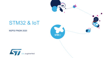
Hardware layout and configuration6UM1956Hardware layout and configurationThe STM32 Nucleo-32 board is based on a 32-pin STM32 microcontroller in LQFP orUFQFPN package.Figure 2 illustrates the connections between the STM32 and its peripherals (ST-LINK/V2-1,push-button, LED, and Arduino Nano connectors).Figure 3: STM32 Nucleo-32 board top layout and Figure 4: STM32 Nucleo-32 board bottomlayout show the location of these connections on the STM32 Nucleo-32 board.Figure 2. Hardware block diagram0LFUR86%670 0LFURFRQWUROOHU,2,25(6(7% 567 UGXLQR 1DQR FRQQHFWRU UGXLQR 1DQR FRQQHFWRU(PEHGGHG 67 /,1. 9 /('/' 06Y 9 10/37UM1956 Rev 5
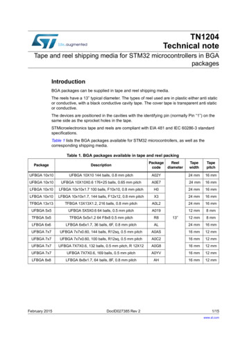
UM19566.1Hardware layout and configurationSTM32 Nucleo-32 board layoutFigure 3. STM32 Nucleo-32 board top layoutCN1ST-LINK Micro BUSB connectorLD1(Red/Green LED)COMCN2ST-LINK SWDconnector(reserved)SB2Connect VCP TX to ST-LINKSB1Power configurationSB3Connect VCP RX to ST-LINKSB8Connect PF1/PC15 to D7SB7Connect PF1/PC15 to X1SB5Connect PF0/PC14 to X1SB6Connect PF0/PC14 to D8U2STM32MicrocontrollerSB4Connect PF0/PC14 to MCOB1Reset ButtonLD3(Green LED)LD2(Red LED) PowerUM1956 Rev 511/3736
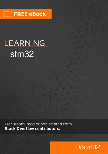
Hardware layout and configurationUM1956Figure 4. STM32 Nucleo-32 board bottom layoutSB9ST-LINK RESETCN4Arduino Nano connectorSB18Connect D4 to A4CN3Arduino Nano connectorSB16Connect D5 to A5SB12Connect BOOT0 to GNDSB11Connect 670 pin 16 toGNDSB13Connect GND to 670 pin32SB10Connect VDD to 670 pin 5SB17Connect MCO to PA0SB143.3V regulator outputJP1IDD measurementSB15Connect D13 to LD312/37UM1956 Rev 5
UM19566.2Hardware layout and configurationSTM32 Nucleo-32 board mechanical drawingFigure 5. STM32 Nucleo-32 board mechanical drawingUM1956 Rev 513/3736
Hardware layout and configuration6.3UM1956Embedded ST-LINK/V2-1The ST-LINK/V2-1 programming and debugging tool is integrated in the STM32 Nucleo-32board. The ST-LINK/V2-1 makes the STM32 Nucleo-32 board mbed enabled.The embedded ST-LINK/V2-1 supports only the SWD for STM32 devices. For informationabout debugging and programming features refer to: ST-LINK/V2 in-circuitdebugger/programmer for STM8 and STM32 User manual (UM1075), which describes indetail all the ST-LINK/V2 features.The new features supported by the ST-LINK/V2-1 comparing with ST-LINK/V2 are: USB software re-enumeration Virtual Com port interface on USB Mass storage interface on USB USB power management request for more than 100 mA power on USBThe features not supported on ST-LINK/V2-1 are: SWIM interface Minimum supported application voltage limited to 3 VKnown limitation: Activating the readout protection on the STM32 target, prevents the target applicationfrom running afterwards. The target readout protection must be kept disabled on STLINK/V2-1 boards.The embedded ST-LINK/V2-1 is directly connected to the SWD port of the target STM32.6.3.1DriversThe ST-LINK/V2-1 requires a dedicated USB driver, which, for Windows 7, 8 and 10, canbe found at www.st.com.In case the STM32 Nucleo-32 board is connected to the PC before the driver is installed,some Nucleo interfaces may be declared as “Unknown” in the PC device manager. In thiscase the user must install the driver files (refer to Figure 6) and from the device managerupdate the driver of the connected device.Note:Prefer using the “USB Composite Device” handle for a full recovery.Figure 6. USB composite device14/37UM1956 Rev 5
UM19566.3.2Hardware layout and configurationST-LINK/V2-1 firmware upgradeThe ST-LINK/V2-1 embeds a firmware upgrade mechanism for in-situ upgrade through theUSB port. As the firmware may evolve during the lifetime of the ST-LINK/V2-1 product (forexample new functionalities added, bug fixes, support for new microcontroller families), it isrecommended to visit www.st.com before starting to use the STM32 Nucleo-32 board andperiodically, to stay up-to-date with the latest firmware version.UM1956 Rev 515/3736
Hardware layout and configuration6.4UM1956Power supply and power selectionThe power supply is provided either by the host PC through the USB cable, or by anexternal source: VIN (7 V-12 V), 5 V (5 V) or 3V3 power supply pins on CN4. In case VIN, 5 V or 3V3 is used to power the STM32 Nucleo-32 board, this power source must complywith the standard EN-60950-1: 2006 A11/2009, and must be Safety Extra Low Voltage(SELV) with limited power capability.In case the power supply is 3V3, the ST-LINK is not powered and cannot be used.6.4.1Power supply input from USB connectorThe STM32 Nucleo-32 board and shield board can be powered from the ST-LINK USBconnector CN1. Note that only the ST-LINK part is power supplied before the USBenumeration phase, as the host PC only provides 100 mA to the boards at that time. Duringthe USB enumeration, the STM32 Nucleo-32 board requires 300 mA of current to the hostPC. If the host is able to provide the required power, the targeted STM32 microcontroller ispowered and the red LED LD2 is turned on, thus the STM32 Nucleo-32 board and its shieldconsume a maximum of 300 mA current and not more. If the host is not able to provide therequired current, the targeted STM32 microcontroller and the shield board are not powersupplied. As a consequence the red LED LD2 stays turned off. In such case it is mandatoryto use an external power supply as explained in the next Section 6.4.2: External powersupply inputs.SB1 is configured according to the maximum current consumption of the board. SB1 can beset to on to inform the host PC that the maximum current consumption does not exceed100 mA (even when Arduino Nano shield is plugged). In such condition USB enumerationwill always succeed since no more than 100 mA is requested to the host PC. Possibleconfigurations of SB1 are summarized in Table 4.Table 4. SB1 configurationSolder bridge stateSB1 OFF (default)SB1 ONSB1 (ON/OFF)Warning:Note:16/37Power supplyUSB power through CN1VIN, 3V3 or 5 V powerAllowed current300 mA max100 mA maxFor current limitation refer to Table 5If the maximum current consumption of the STM32 Nucleo-32board and its shield board exceed 300 mA, it is mandatory topower the STM32 Nucleo-32 board, using an external powersupply connected to VIN, 5 V or 3V3.In case the board is powered by a USB charger, there is no USB enumeration, so the LEDLD2 remains set to off permanently and the target STM32 is not powered. In this specificcase the SB1 must be set to on, to allow the target STM32 to be powered anyway.UM1956 Rev 5
UM19566.4.2Hardware layout and configurationExternal power supply inputsThe STM32 Nucleo-32 board and its shield boards can be powered in three different waysfrom an external power supply, depending on the voltage used. The three power sourcesare summarized in the Table 5.Table 5. External power sourcesInput powernameConnectorpinVoltagerangeMax currentLimitationVINCN4 pin 17 V to 12 V800 mAFrom 7 V to 12 V only and inputcurrent capability is linked to inputvoltage:800 mA input current when VIN 7 V450 mA input current when7 V VIN 9 V300 mA input current when10 V VIN 9 Vless than 300 mA input current whenVIN 10 V 5 VCN4 pin 44.75 V to5.25 V500 mAST-LINK not powered 3V3CN4 pin 143 V to 3.6 V-ST-LINK not powered and SB14 andSB9 must be off.VIN or 5 V power supplyWhen powered from VIN or 5 V, it is still possible to use ST-LINK for communication forprogramming or debugging only, but it is mandatory to power the board first, using VIN or 5 V, then to connect the USB cable to the PC. By this way the enumeration will succeedanyway, thanks to the external power source.The following power sequence procedure must be respected:1.Check that SB1 is off2.Connect the external power source to VIN or 5 V3.Power on the external power supply 7 V VIN 12 V to VIN, or 5 V for 5 V4.Check red LED LD2 is turned on5.Connect the PC to USB connector CN1If this order is not respected, the board may be powered by VBUS first, then by VIN or 5 V,and the following risks may be encountered:1.If more than 300 mA current is needed by the board, the PC may be damaged orcurrent supplied is limited by the PC. As a consequence the board is not poweredcorrectly.2.300 mA is requested at enumeration (since SB1 must be off) so there is the risk thatthe request is rejected and the enumeration does not succeed if the the PC cannotprovide such current. Consequently the board is not power supplied (LED LD2 remainsoff).UM1956 Rev 517/3736
Hardware layout and configurationUM1956 3V3 power supplyUsing the 3V3 (CN4 pin 14) directly as power input, can be interesting, for instance, incase the 3.3 V is provided by a shield board. In this case the ST-LINK is not powered, thusprogramming and debugging features are not available. When the board is powered by 3V3 (CN4 pin 14), the solder bridge SB14 and SB9 (NRST) must be off.6.4.3External power supply outputWhen powered by USB or VIN, the 5 V (CN4 pin 4) can be used as output power supplyfor an Arduino Nano shield. In this case, the maximum current of the power source specifiedin Table 5: External power sources must be respected.The 3.3 V (CN4 pin 14) can be used also as power supply output. The current is limited bythe maximum current capability of the regulator U3 (500 mA max).6.5LEDsThe tricolor LED (green, orange, red) LD1 (COM) provides information about ST-LINKcommunication status. LD1 default color is red. LD1 turns to green to indicate that thecommunication is in progress between the PC and the ST-LINK/V2-1, with the followingsetup: Slow blinking red/off: at power-on before USB initialization Fast blinking red/off: after the first correct communication between PC and STLINK/V2-1 (enumeration) Red on: when initialization between PC and ST-LINK/V2-1 is completed Green on: after a successful target communication initialization Blinking red/green: during communication with target Green on: communication finished and successful Orange on: communication failureUser LD3: the green LED is a user LED connected to Arduino Nano signal D13corresponding to the STM32 I/O PB3 (pin 26). Refer to Table 9, Table 10, Table 12,Table 13, Table 14, Table 15 and Table 16 for concerned STM32: When the I/O is HIGH value, the LED is on When the I/O is LOW, the LED is offPWR LD2: the red LED indicates that the STM32 part is powered and 5 V power isavailable.6.6Push-buttonB1 RESET: the push-button is connected to NRST, and it is used to reset the STM32.18/37UM1956 Rev 5
UM19566.7Hardware layout and configurationJP1 (IDD)JP1, labeled IDD, is used to measure the STM32 microcontroller consumption by removingthe jumper and connecting an ammeter: JP1 on: STM32 is powered (default) JP1 off: an ammeter must be connected to measure the STM32 currentIf there is no ammeter, STM32 is not powered.6.8OSC clockU2 pin 2 and pin 3 can be used as OSC clock input or as Arduino Nano D8 and D7 GPIO.There are four ways to configure the pins corresponding to different STM32 and clock usage(refer to Table 6).Table 6. OSC clock configurationsSolder bridgeSB4SB17SB6SB8SB5 andSB7ONOFFOFFONOFFSTM32STM32FxxxClock configurationMCO from ST-LINKconnected to OSCIN(PF0) (1)OFFOFFONONOFFHSI configuration(default configuration)OFFONOFFOFFOFFMCO from ST-LINKconnected to CKIN(PA0)(1)STM32LxxxOFFOFFOFFOFFON32K LSE mounted on X1(default configuration)OFFOFFONON/OFFOFFArduino Nano D7connected to PF0 / PC14AllOFFOFFON/OFFONOFFArduino Nano D8connected to PF1 / PC151. In applications where VCP is used for communication at a speed higher than 9600 bauds, it may beneeded to use this solder bridge configuration, to use 8 MHz clock (MCO from ST-LINK) and get a moreprecise frequency.Boards with STM32Lxxx are delivered with 32.768 KHz crystal (X1). Associated capacitorsand solder bridges (C12, C13 and SB4 to SB8) are configured to support LSE by default.Boards with STM32Fxxx are delivered without crystal (X1). Associated capacitors (C12,C13) are not populated and SB4 to SB8 are configured to support HSI by default.UM1956 Rev 519/3736
Hardware layout and configuration6.9UM1956USART virtual communicationThanks to SB2 and SB3, the USART interface of STM32 available on PA2 (TX) and PA15(RX), can be connected to ST-LINK/V2-1. When USART is not used it is possible to use PA2as Arduino Nano A7. Refer to Table 7.Table 7. Virtual communication configurationBridgeState(1)SB2SB3DescriptionOFFPA2 is connected to CN4 pin 5 as Arduino Nano analog input A7 anddisconnected from ST-LINK USART.ONPA2 is connected to ST-LINK as virtual Com TX (default).OFFPA15 is not connected.ONPA15 is connected to ST-LINK as virtual Com RX (default).1. The default configuration is reported in bold style.6.10Solder bridgesTable 8. Solder bridgesBridgeSB10 (VREF )SB15 (LD3-LED)State(1)ONVREF on STM32 is connected to VDD.OFFVREF on STM32 is not connected to VDD and it is provided bypin 13 of CN4.ONGreen user LED LD3 is connected to D13 of Arduino Nano signal.OFFGreen user LED LD3 is not connected.ONThe NRST signal of ST-LINK is connected to the NRST pin of theSTM32.OFFThe NRST signal of ST-LINK is not connected to the NRST pin ofthe STM32, when used external power ( 3V3, 5 V) as powersupply.ONPin 16 of STM32 (U2) is connected to VSS.OFFPin 16 of STM32 (U2) is not connected to VSS, and used as GPIOPB2 for STM32F031.ONPin 32 of STM32 (U2) is connected to VSS.OFFPin 32 of STM32 (U2) is not connected to VSS, and used as GPIOPB8 for STM32F031.ONPin 31 of STM32 (U2) is connected to GND via 10K pull-down andused as BOOT0.OFFPin 16 of STM32 (U2) is not connected and is GPIO PB8 forSTM32F042.ONSTM32 PB6 is connected to CN4 pin 7 for I2C SDA support onArduino Nano A5. In such case STM32 PB6 does not supportArduino Nano D5 and PA6 must be configured as input floating.SB9 (NRST)SB11 (PB2/VSS)SB13 (PB8/VSS)SB12 (PB8/BOOT0)SB1620/37DescriptionUM1956 Rev 5
UM1956Hardware layout and configurationTable 8. Solder bridges (continued)BridgeState(1)SB16OFFCN4 pin 7 is used as Arduino Nano analog input A5 without I2Csupport and CN3 pin 8 is available as Arduino Nano D5.ONSTM32 PB7 is connected to CN4 pin 8 for I2C SCL support onArduino Nano A4. In such case STM32 PB7 does not supportArduino Nano D4 and PA5 must be configured as input floating.OFFCN4 pin 8 is used as Arduino Nano analog input A4 without I2Csupport and CN3 pin 7 is available as Arduino Nano D4.SB18Description1. The default configuration is reported in bold style.6.11Arduino Nano connectorsCN3 and CN4 are male connectors compatible with Arduino Nano standard. Most shieldsdesigned for Arduino Nano can fit the STM32 Nucleo-32 board.Caution:The I/Os of STM32 are 3.3 V compatible instead of 5 V for Arduino Nano.Table 9, Table 10, Table 12, Table 13, Table 14, Table 15 and Table 16 show the pinassignments of each STM32 on Arduino Nano connectors.Figure 7 and Figure 8 show Arduino Nano connectors and pin assignments forNUCLEO-F031K6, NUCLEO-F042K6, NUCLEO-F303K8, NUCLEO-L011K4, NUCLEOL031K6 and NUCLEO-L432KC.Table 9. Arduino Nano connectors on NUCLEO-F031K6ConnectorPin numberPin nameSTM32 pinFunctionLeft connectorCN31D1PA9USART1 TX(1)2D0PA10USART1 RX(1)3RESETNRSTRESET4GND-Ground5D2PA12-6D3PB0TIM3 CH37D4(5)PB7-8D5(5)PB6TIM16 CH1N(2)9D6PB1TIM14 CH110D7(3)PF0-11D8(3)PF1-12D9PA8TIM1 CH113D10PA11SPI CS(4) TIM1 CH414D11PB5SPI1 MOSI TIM3 CH215D12PB4SPI1 MISOUM1956 Rev 521/3736
Hardware layout and configurationUM1956Table 9. Arduino Nano connectors on NUCLEO-F031K6 (continued)ConnectorPin numberPin nameSTM32 pinFunctionRight connectorCN4CN41VIN-Power input2GND-Ground3RESETNRSTRESET4 5V-5 V input/output5A7PA2ADC IN26A6PA7ADC IN77(5)A5PA6ADC IN6 I2C1 SCL8A4(5)PA5ADC IN5 I2C1 SDA9A3PA4ADC IN410A2PA3ADC IN311A1PA1ADC IN112A0PA0ADC IN013AREF-AVDD14 3V3-3.3 V input/output15D13PB3SPI1 SCK1. Only one USART is available and it is shared between Arduino Nano and VCP. The selection is done byremapping (no need to change the hardware configuration).2. D5 PWM on inverted channel Timer 16.3. D7/D8 shared with OSC IN/OSC OUT.4. SPI CS is made by GPIO.5. Limitations on A4 and A5, D4 and D5, related to I2C configuration, are explaine
User manual. STM32 Nucleo-32 boards (MB1180) Introduction. . Arduino Nano connectivity support makes it easy to expand the functionality of the . The STM32 Nucleo-32 board is a low-cost and easy-to-use development kit used to quickly evaluate and start a development with an STM32 microcontroller in LQFP32 or UFQFPN32