Transcription
AN4776Application noteGeneral-purpose timer cookbook for STM32 microcontrollersIntroductionThe timer peripheral is part of the essential set of peripherals embedded in all the STM32microcontrollers. The number of timer peripherals and their respective features differ fromone STM32 microcontroller family to another, but they all share some common features andoperating modes.The STM32 timer peripheral was conceived to be the keystone peripheral for a largenumber of applications: from motor-control applications to periodic-events generationapplications. The specifications on the timer peripheral available in all STM32 referencemanuals are very wide due to its versatility.The purpose of this application note is to provide a simple and clear description of the basicfeatures and operating modes of the STM32 general-purpose timer peripherals. Thisdocument complements the specifications of the STM32 timer peripherals available on theirreference manuals.The document is divided in two main parts: The first section presents the basic features of the STM32 timers in a simple way anddescribes some specific features that are commonly used within timer-peripheral-basedapplications. The following sections are dedicated to describe a particular use-case of an STM32 timerperipheral. These sections provide a deep description of the main STM32 timer featuresused to build the example application. They also describe the architecture of the usedsource code.The objective of this application note is to present in a generic and simple way some usecases of the STM32 timer peripherals, and it does not cover use-cases like motor controlapplications due to their complexity.July 2019AN4776 Rev 31/72www.st.com1
AN47761Basic operating modes of STM32 general-purpose timers . . . . . . . . . . 51.1Introduction . . . . . . . . . . . . . . . . . . . . . . . . . . . . . . . . . . . . . . . . . . . . . . . . 51.2STM32 timer peripheral tear-down . . . . . . . . . . . . . . . . . . . . . . . . . . . . . . . 51.31.42342/721.2.1The master/slave controller unit . . . . . . . . . . . . . . . . . . . . . . . . . . . . . . . . 71.2.2The time-base unit . . . . . . . . . . . . . . . . . . . . . . . . . . . . . . . . . . . . . . . . . . 71.2.3The timer-channels unit . . . . . . . . . . . . . . . . . . . . . . . . . . . . . . . . . . . . . . 81.2.4The Break feature unit . . . . . . . . . . . . . . . . . . . . . . . . . . . . . . . . . . . . . . 10STM32 timer peripheral basic operating modes . . . . . . . . . . . . . . . . . . . . 101.3.1Timer time-base configuration . . . . . . . . . . . . . . . . . . . . . . . . . . . . . . . . 101.3.2Timer channel-configuration in input mode . . . . . . . . . . . . . . . . . . . . . . 111.3.3Timer channel-configuration in output mode . . . . . . . . . . . . . . . . . . . . . 11STM32 timer peripheral advanced features . . . . . . . . . . . . . . . . . . . . . . . 121.4.1Filtering stage . . . . . . . . . . . . . . . . . . . . . . . . . . . . . . . . . . . . . . . . . . . . 121.4.2The preload feature of the timer registers . . . . . . . . . . . . . . . . . . . . . . . 13Timer clocking using external clock-source . . . . . . . . . . . . . . . . . . . . 162.1Overview . . . . . . . . . . . . . . . . . . . . . . . . . . . . . . . . . . . . . . . . . . . . . . . . . 162.2Synchronization block . . . . . . . . . . . . . . . . . . . . . . . . . . . . . . . . . . . . . . . 172.3The external clock-source mode 1 . . . . . . . . . . . . . . . . . . . . . . . . . . . . . . 182.4The external clock-source mode 2 . . . . . . . . . . . . . . . . . . . . . . . . . . . . . . 202.5External clock-source mode 1 versus mode 2 . . . . . . . . . . . . . . . . . . . . . 222.6Application: timer clocking using external clock-sourceon ETR timer input . . . . . . . . . . . . . . . . . . . . . . . . . . . . . . . . . . . . . . . . . 232.7Firmware overview. . . . . . . . . . . . . . . . . . . . . . . . . . . . . . . . . . . . . . . . . 31N-pulse waveform generation using one-pulse mode . . . . . . . . . . . . . 333.1Overview . . . . . . . . . . . . . . . . . . . . . . . . . . . . . . . . . . . . . . . . . . . . . . . . . 333.2Application: N-pulse waveform generation using one-pulse mode . . . . . 343.3Firmware overview . . . . . . . . . . . . . . . . . . . . . . . . . . . . . . . . . . . . . . . . . . 36Cycle-by-cycle regulation using break input . . . . . . . . . . . . . . . . . . . . 374.1Overview . . . . . . . . . . . . . . . . . . . . . . . . . . . . . . . . . . . . . . . . . . . . . . . . . 374.2Break input versus OCxRef-clear utilization . . . . . . . . . . . . . . . . . . . . . . . 374.3Application: cycle-by-cycle regulation using the Break feature . . . . . . . . 394.4Firmware overview . . . . . . . . . . . . . . . . . . . . . . . . . . . . . . . . . . . . . . . . . . 42AN4776 Rev 3
AN477656Arbitrary waveform generation using timer DMA-burst feature . . . . . 445.1STM32 DMA-burst feature overview . . . . . . . . . . . . . . . . . . . . . . . . . . . . 445.2Timer DMA-burst feature . . . . . . . . . . . . . . . . . . . . . . . . . . . . . . . . . . . . . 445.3Application example: arbitrary waveform generation usingtimer DMA-burst feature . . . . . . . . . . . . . . . . . . . . . . . . . . . . . . . . . . . . . 48N-pulse waveform generation using timer synchronization . . . . . . . . 566.1Timer synchronization overview . . . . . . . . . . . . . . . . . . . . . . . . . . . . . . . . 566.2N-pulse waveform generation application example - part 1 . . . . . . . . . . . 586.3N-pulse waveform generation application example - part2 . . . . . . . . . . . 636.3.17Clock configuration . . . . . . . . . . . . . . . . . . . . . . . . . . . . . . . . . . . . . . . . 66Revision history . . . . . . . . . . . . . . . . . . . . . . . . . . . . . . . . . . . . . . . . . . . 71AN4776 Rev 33/723
List of figuresAN4776List of figuresFigure 1.Figure 2.Figure 3.Figure 4.Figure 5.Figure 6.Figure 7.Figure 8.Figure 9.Figure 10.Figure 11.Figure 12.Figure 13.Figure 14.Figure 15.Figure 16.Figure 17.Figure 18.Figure 19.Figure 20.Figure 21.Figure 22.Figure 23.Figure 24.Figure 25.Figure 26.Figure 27.Figure 28.Figure 29.Figure 30.Figure 31.Figure 32.Figure 33.Figure 34.Figure 35.Figure 36.Figure 37.Figure 38.Figure 39.Figure 40.4/72TIM1 timer-peripheral block diagram . . . . . . . . . . . . . . . . . . . . . . . . . . . . . . . . . . . . . . . . . . 6Relevant bloc diagram for the timer channel when configured as output . . . . . . . . . . . . . . . 8Relevant bloc diagram for the timer channel when configured as input . . . . . . . . . . . . . . . 10Input signal filtering (ETF [3:0] 0100) : FSAMPLING FDTS/2, N 6. . . . . . . . . . . . . . . . 12Preload mechanism for timer channel register - disabled. . . . . . . . . . . . . . . . . . . . . . . . . . 14Preload mechanism for timer channel register - enabled . . . . . . . . . . . . . . . . . . . . . . . . . . 14Synchronizing an STM32 timer by an external clock-signal . . . . . . . . . . . . . . . . . . . . . . . . 16Clock path for external clock-source modes . . . . . . . . . . . . . . . . . . . . . . . . . . . . . . . . . . . . 17Synchronization block . . . . . . . . . . . . . . . . . . . . . . . . . . . . . . . . . . . . . . . . . . . . . . . . . . . . . 18Timer counter increment (external clock mode 1). . . . . . . . . . . . . . . . . . . . . . . . . . . . . . . . 20Timer counter increment (external clock mode 2) . . . . . . . . . . . . . . . . . . . . . . . . . . . . . . . 21Synoptic of a frequency meters . . . . . . . . . . . . . . . . . . . . . . . . . . . . . . . . . . . . . . . . . . . . . 24Frequency meter architecture clocked by the internal HSI oscillator . . . . . . . . . . . . . . . . . 26Frequency meter architecture clocked by the external clock-source mode 2 . . . . . . . . . . . 27Timing diagram of input capture . . . . . . . . . . . . . . . . . . . . . . . . . . . . . . . . . . . . . . . . . . . . . 28The PPM resulting of the internal source clock . . . . . . . . . . . . . . . . . . . . . . . . . . . . . . . . . 30The PPM resulting of the external source clock . . . . . . . . . . . . . . . . . . . . . . . . . . . . . . . . . 31Project organization . . . . . . . . . . . . . . . . . . . . . . . . . . . . . . . . . . . . . . . . . . . . . . . . . . . . . . 32Example of one-pulse mode . . . . . . . . . . . . . . . . . . . . . . . . . . . . . . . . . . . . . . . . . . . . . . . . 34Architecture example . . . . . . . . . . . . . . . . . . . . . . . . . . . . . . . . . . . . . . . . . . . . . . . . . . . . . 35Firmware source code organization . . . . . . . . . . . . . . . . . . . . . . . . . . . . . . . . . . . . . . . . . . 36Timing of clearing TIMx OCxREF . . . . . . . . . . . . . . . . . . . . . . . . . . . . . . . . . . . . . . . . . . . . 38Timing of Break function . . . . . . . . . . . . . . . . . . . . . . . . . . . . . . . . . . . . . . . . . . . . . . . . . . . 38Timing of cycle-by-cycle regulation. . . . . . . . . . . . . . . . . . . . . . . . . . . . . . . . . . . . . . . . . . . 39Cycle-by-cycle regulation architecture . . . . . . . . . . . . . . . . . . . . . . . . . . . . . . . . . . . . . . . . 40Oscilloscope screen-shot for the obtained waveform . . . . . . . . . . . . . . . . . . . . . . . . . . . . . 41Project organization . . . . . . . . . . . . . . . . . . . . . . . . . . . . . . . . . . . . . . . . . . . . . . . . . . . . . . 43Configuration for a timer DMA-burst transfer sequence . . . . . . . . . . . . . . . . . . . . . . . . . . . 46Synoptic schema of arbitrary waveform generation using DMA-burst . . . . . . . . . . . . . . . . 48Arbitrary waveform generator application: targeted waveform . . . . . . . . . . . . . . . . . . . . . . 49Waveform generation data pattern stored in microcontroller memory . . . . . . . . . . . . . . . . 51Block diagram of arbitrary waveform generation example . . . . . . . . . . . . . . . . . . . . . . . . . 52Arbitrary signal generation on channel1 of TIM1 timer . . . . . . . . . . . . . . . . . . . . . . . . . . . . 53Periodic N-pulses generation block diagram . . . . . . . . . . . . . . . . . . . . . . . . . . . . . . . . . . . 58Output waveform target of periodic N-pulses generation example . . . . . . . . . . . . . . . . . . . 59Periodic N-pulses generation synoptic schema . . . . . . . . . . . . . . . . . . . . . . . . . . . . . . . . . 59Timing diagram of periodic N-pulses generation example . . . . . . . . . . . . . . . . . . . . . . . . . 60Synoptic schema of two complementary N pulses waveform generation example . . . . . . 64Output of two N-pulses complimentary waveforms generation example . . . . . . . . . . . . . . 64Timing diagram of complimentary N-pulses waveforms generation with similar final state 67AN4776 Rev 3
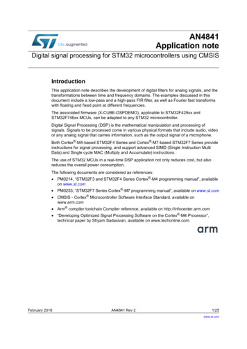
AN4776Basic operating modes of STM32 general-purpose timers1Basic operating modes of STM32 general-purposetimers1.1IntroductionAll of the STM32 microcontroller embeds at least one timer peripheral and some of themembed more than one type of timer peripherals. This document covers the general purposeones. The general purpose timers can be recognized from other types of STM32 timerperipherals by their name.Within the STM32 microcontrollers’ documentation, a general purpose timer peripheral isalways named “TIMx timer”, where “x” can be any number and it does not reflect the numberof timer peripherals embedded by a given microcontroller. For example, the STM32F100microcontrollers embed a timer peripheral named TIM17, but the total number of timerperipherals embedded by these microcontrollers is less than 17.In general, across the STM32 microcontrollers families, the timer peripherals that have thesame name also have the same features set, but there are a few exceptions. For example,the TIM1 timer peripheral is shared across the STM32F1 Series, STM32F2 Series andSTM32F4 Series, but for the specific case of STM32F30x microcontrollers family, the TIM1timer peripheral features a bit richer features set than the TIM1 present in the other families.The general purpose timers embedded by the STM32 microcontrollers share the samebackbone structure; they differ only on the level of features embedded by a given timerperipheral. The level of features integration for a given timer peripheral is decided based onthe applications field that it targets.The timer peripherals can be classified as: Advanced-configuration timers like TIM1 and TIM8 among others. General-purpose configuration timers like TIM2 and TIM3 among others Lite-configuration timers like TIM9, TIM10, TIM12 and TIM16 among others Basic-configuration timers like TIM6 and TIM7 among others.The application note STM32 cross-series timer overview (AN4013) presents a detailedoverview on the STM32 timer peripherals across the different STM32 microcontrollerfamilies.1.2STM32 timer peripheral tear-downAll the STM32 general-purpose timer peripherals share the same backbone structure. Thissection tears down the advanced configuration TIM1 timer peripheral, which is the timerperipheral with the most features.Figure 1 shows the block diagram for the TIM1 timer peripheral. The STM32 timerperipheral is made by the assembly of four units:1.The master/slave controller unit2.The time-base unit3.The timer channels unit4.The Break feature unit.AN4776 Rev 35/7271
Basic operating modes of STM32 general-purpose timersAN4776Figure 1. TIM1 timer-peripheral block diagramInternal clock (CK INT)CK TIM18 from RCCETRFETRTIMx ETRTriggercontrollerTRGOETRPPolarity selection & edgedetector & InputprescalerfilterITR0ITR1ITR2ITR3to other timersto DAC/ADCTGIITRTRCTRGISlavecontrollermodeReset, enable, up/down, countTI1F EDEncoderInterfaceTI1FP1TI2FP2REP registerUUIAuto-reload registerRepetitioncounterStop, clear or up/downCK PSCXORTI1TIMx CH1Input filter &edge detectorTI1FP1TI1FP2CK CNTPSCprescalerCC1I UIC1PrescalerTRCIC1PS /-CNT counterCC1ICapture/Compare 1 registerCC2ITI2Input filter &edge mpare 2 registerTIMx CH3Input filter &edge detectorTI3FP3TI3FP4IC3PrescalerTRCIC3PSTI4Input filter &edge detectorTI4FP3TI4FP4TRCOutputcontrolOC1TIMx CH1NOC1NTIMx CH2OC2REFDTGOutputcontrolOC2TIMx CH2NCC3ICapture/Compare 3 registerCC4IIC4PrescalerIC4PSTIMx CH3OC3REFDTGCC4IUTIMx CH4TIMx CH1DTGOC2NCC3I UTI3DTG registersOC1REFCC2IUTIMx CH2UOutputcontrolOC3TIMx CH3NOC3NCapture/Compare 4 registerOC4REFOutput OC4controlCapture/Compare 5 registerOC5REFOutput OC5controlCapture/Compare 6 registerOC6REFOutput OC6controlTIMx CH4Internal sourcesETRFTIMx BKINBreak and Break2 circuitry (1)TIMx BKIN2Notes:RegMaster/slave controllerRegTime-baseRegTimer channelsRegBreak featureMS34408V26/72AN4776 Rev 3
AN47761.2.1Basic operating modes of STM32 general-purpose timersThe master/slave controller unitThe master/slave unit provides the time-base unit with the counting clock signal (forexample the CK PSC signal), as well as the counting direction control signal. This unitmainly provides the control signals for the time-base unit.The master/slave controller decides the right counting configuration for the time-base unitbased on the timer master/slave configuration; it also decides the actual counting status.For example, if the timer is configured in one of the encoder modes by writing the right valueinto the SMS control bit-field within the TIMx SMCR timer register, then the counting clocksignal and the counting-direction control signal is computed based on the state of theTI1FP1 and TI2FP2 input signals.The master/slave controller unit handles the inter-timers synchronization. This unit can beconfigured to output a synchronization signal (TRGO signal) next to a certain timer internalevent. It can be configured as well to control the time-base counter in function of externalevents (like internal events of other timers or external signals).It is possible to configure one slave timer to increment its counter based on a master-timerevents such as the timer update event. In this example the master-timer event is signaled bythe master timer master/slave controller unit. This controlling unit uses the master timeroutput-TRGO signal. The master timer output-TRGO signal is connected to the slave timerTRGI-input signal. The master/slave controller unit of the slave timer is configured to use theTRGI-input signal as clock source to increment the slave timer counter.Not all the STM32 timer peripherals feature the same master/slave controller capabilities.The TIM1 timer peripheral taken as example, embeds the full master/slave capabilities;contrary to the TIM6 and TIM7 basic timers that embed the simplest master/slave controller.The master/slave controller within the TIM6 and TIM7 timer peripherals has no control bitfiled.For the TIM6 and TIM7 timer peripherals, the time-base counter is always up-counting withno means to reset its content next to external events. It is not possible either to clock themwith a different clock source nor with the timer peripheral internal clock.1.2.2The time-base unitThe time-base unit is made by the timer counter in addition to a prescaler stage and arepetition counter. The clock signal fed into the time-base unit passes first through aprescaling stage before reaching the time-base counter.Depending on the content of the TIMx PSC timer prescaler register, the counting signalfrequency may be scaled down before reaching the counter stage. The output signal of theprescaling stage is the clock counting signal for the timer counter stage.The timer counter is controlled by two timer registers: The TIMx CNT timer register is used to read and write the content of the timer counter. The TIMx ARR timer register contains the reload value of the timer counter.–If the timer counter is up-counting and it reaches the content of the timer autoreload register (TIMx ARR), then the timer counter resets itself and a newcounting cycle is restarted.–If the timer counter is down-counting and it reaches the zero value, then the timercounter value is set to the content of the timer auto-reload register (TIMx ARR)and a new counting cycle is restarted.AN4776 Rev 37/7271
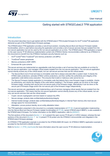
Basic operating modes of STM32 general-purpose timersAN4776Each time a new counting cycle is restarted, a timer “update event” is triggered as long asthe content of the repetition counter is null. If the content of the repetition counter is not null,then no “update event” is triggered, but a new counting cycle is restarted and the content ofthe repetition counter is decreased by one. Next to each “update event” the content of therepetition counter is set to the value stored by the TIMx RCR timer register.Not all the STM32 timer peripherals embed the repetition counter. If the repetition counter isnot embedded, then the timer peripheral would behave as if the repetition counter isembedded but its content is null.1.2.3The timer-channels unitThe timer channels are the working elements of the timer; they are the means by which atimer peripheral interacts with its external environment. In general, the timer channels aremapped to the STM32 microcontroller pins with few exceptions such as the timer channel 5and 6 for the TIM1 timer peripheral on the STM32F30x microcontrollers family. A timerchannel mapped to an STM32 microcontroller pin can be used either as an input or as anoutput.Timer channel configured as outputWhen configured as an output, the timer channel is used to generate a set of possiblewaveforms. As long as the channel is configured in output mode, the content of theTIMx CCRy channel register is compared to the content of the timer counter.Based on the results of this continuous logic comparison and based on the configuredoutput sub-mode (like PWM1 mode or Inactive mode), the timer channel internal outputOCyREF is either set or reset.The timer channel internal output OCyREF is then fed into the channel output stage. Thechannel output stage applies a set of conditioning operations on the OCyREF signal basedon a set of configured parameters (like channel polarity configuration or dead-timegeneration among others).The output signal of the channel output stage is mapped to the microcontroller pins asalternate function. Note that some output stages of timer channels, as the one representedin Figure 2, may output two complementary signals.The control bit-fields for such channel output stage provides the means to configure eachoutput signal separately (like enabled/disabled output signal or like polarity).Figure 2. Relevant bloc diagram for the timer channel when configured as outputCNT counterLogical comparisonCCyDTG[7:0] registersTIMx CHyOCyREFCapture/Compare y registerDTGBreak controlOutputcontrolOCyTIMx CHyNOCyNMSv41561V18/72AN4776 Rev 3
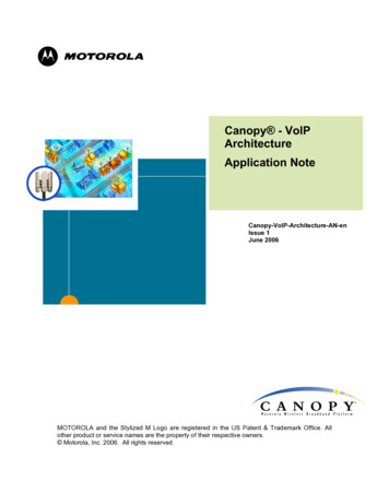
AN4776Basic operating modes of STM32 general-purpose timersTimer channel configured as an inputWhen configured as an input, the timer channel can be used to time-stamp the rising and/orthe falling edge of external signals. To handle this function, the channel input is mapped toone of the microcontroller pins.Some timer-channel inputs are mapped as well to some on-chip signals, for example theoscillator output for calibration purposes. The TIy timer channel input feeds the channelinput conditioning circuitry as shown in Figure 3. The conditioning circuitry includes afiltering stage and an edge detector. The filter stage rejects pulses with duration less thanthe configured one. The edge detector detects if an active edge occurred on the concernedtimer input after filtering.The active edge configuration is set by writing to the channel polarity control bit-fields withinthe TIMx CCER timer register. The conditioning circuitry outputs two signals: The TIyFPy: is the TIy timer input signal which was filtered and on which an activeedge is detected depending on the polarity of the timer channel “y”. The TIyFPz: is always the TIy timer input signal which was filtered but on which anactive edge is detected depending on the polarity of the timer channel “z”.The TIyFPz signal is redirected to the prescaler input of the channel “z” where the TIzFPysignal is redirected to the prescaler input of the channel “y” as shown in Figure 3. This crossswap of filtered input signals is very useful for time-stamping both the rising and the fallingedges of an input signal. It is very useful for implementing PWM (pulse width modulation)input applications.Each timer channel can be configured in one of three possible input modes. Each inputmode corresponds to one of the possible three inputs of the prescaler mux connected to thetimer channel prescaler. The CCyS control bit-field controls if the timer channel is configuredin output mode (like CCyS[1:0] ‘00’) or if it is configured in one of the input modes (likeCCyS[1:0] different from ‘00’).The same TIMx CCMRn timer registers (‘n’ can be any number, but generally is either 1 or2) are used to configure the timer channels either as input or as output. Some control bitfields of the TIMx CCMRn timer registers have different interpretation based on the channelconfiguration, input or output modes.The timer channel prescaler may be configured to scale down the frequency of the activeedges detected on the timer input TIy. The detection of an active edge on the output of thechannel prescaler triggers the transfer of the timer counter content to the “y” register of theTIMx CCRy timer channel.The content of the “y” register of the TIMx CCRy timer channel is the timestamp of the lastdetected active edge on the output of the channel “y” prescaler. It is the timestamp of thelast detected active edge on the TIy timer input if the channel “y” prescaler is configured tonot scale down the input signal (for example when the prescaler ratio 1, in other words,channel prescaler is bypassed).AN4776 Rev 39/7271
Basic operating modes of STM32 general-purpose timersAN4776Figure 3. Relevant bloc diagram for the timer channel when configured as inputTIYInput filter &edge detectorTIMx CHyCCyIUTIyFPyTIyFPzTRCTo adjacent channel ZICyPrescalerICyPS /-CNT counterCapture/Compare y RegisterFrom adjacent channel ZMS34408V51.2.4The Break feature unitThe Break feature unit is embedded only by timer peripherals that feature complementaryoutputs. In other words, only timer peripherals that have at least one channel with twocomplimentary outputs embed the Break feature.The Break feature acts on the output stage of timer channels configured in output mode. Assoon as an active edge is detected on the break input, the outputs of timer channelsconfigured in output mode are either turned off or forced to a predefined safe state.The Break feature is typically used for implementing safe shutdown functionality in electricalpower inverters next to anomalies.The application note Using STM32 device PWM shut-down features for motor control anddigital power conversion (AN4277) provides a detailed description of the Break featureacross the STM32 microcontroller families.1.3STM32 timer peripheral basic operating modesThis section provides a set of source code snippets for a set of basic configurations of theSTM32 timer peripheral. These snippets were developed using the C programminglanguage.1.3.1Timer time-base configuration#define ANY DELAY RQUIRED0x0FFF/* Hardware-precision delayperipheral. Any other STM32TIM6 timer was chosen as itperipherals may be reservedloop implementation using TIM6 timertimer can be used to fulfill this function, buthas the less integration level. Other timerfor more complicated tasks *//* Clear the update event flag */TIM6- SR 0/* Set the required delay *//* The timer presclaer reset value is 0. If a longer delay is required thepresacler register may be configured to *//*TIM6- PSC 0 */TIM6- ARR ANY DELAY RQUIRED/* Start the timer counter */TIM6- CR1 TIM CR1 CEN10/72AN4776 Rev 3
AN4776Basic operating modes of STM32 general-purpose timers/* Loop until the update event flag is set */while (!(TIM6- SR & TIM SR UIF));/* The required time delay has been elapsed *//* User code can be executed */1.3.2Timer channel-configuration in input mode/* Variable to store timestamp for last detected active edge */uint32 t TimeStamp;/* The ARR register reset value is 0x0000FFFF for TIM3 timer. So it shouldbe ok for this snippet *//* If you want to change it uncomment the below line *//* TIM3- ARR ANY VALUE YOU WANT *//* Set the TIM3 timer channel 1 as input *//* CC1S bits are writable only when the channel1 is off *//* After reset, all the timer channels are turned off */TIM3- CCMR1 TIM CCMR1 CC1S 0;/* Enable the TIM3 channel1 and keep the default configuration (state afterreset) for channel polarity */TIM3- CCER TIM CCER CC1E;/* Start the timer counter */TIM3- CR1 TIM CR1 CEN;/* Clear the Capture event flag for channel 1 */TIM3- SR TIM SR CC1IF;/* Loop until the capture event flag is set */while (!(TIM3- SR & TIM SR CC1IF));/* An active edge was detected, so store the timestamp */TimeStamp TIM3- CCR1;1.3.3Timer channel-configuration in output mode/* The ARR register reset value is 0x0000FFFF for TIM3 timer. So it shouldbe ok for this snippet. If you want to change it uncomment the below line *//* TIM3- ARR ANY VALUE YOU WANT *//* The TIM3 timer channel 1 after reset is configured as output *//* TIM3- CC1S reset value is 0 *//* To select PWM2 output mode set the OC1M control bit-field to '111' */TIM3- CCMR1 TIM CCMR1 OC1M 0 TIM CCMR1 OC1M 1 TIM CCMR1 OC1M 2;/* Set the duty cycle to 50% */TIM3- CCR1 TIM3- ARR / 2;/* By default, after reset, preload for channel 1 is turned off *//* To change it uncomment the below line *//* TIM3- CCMR1 TIM CCMR1 OC1PE;/* Enable the TIM3 channel1 and keep the default configuration (state afterreset) for channel polarity */TIM3- CCER TIM CCER CC1E;/* Start the timer counter */AN4776 Rev 311/7271
Basic operating modes of STM32 general-purpose timersAN4776TIM3- CR1 TIM CR1 CEN1.4STM32 timer peripheral advanced featuresThis section provides a detailed description of some common STM32 timer features used byapplication examples detailed later in this document.1.4.1Filtering stageTimer inputs (like ETR input or channel inputs) feature a filtering stage that may be activatedto filter out external signal pulses with duration less than a desired threshold.The maximal duration of filtered pulses depends on two parameters: The configuration of the filtering stage respective to a certain timer input. For example,the ETR input filtering stage is configured through the ETF[3:0] control bit-field withinthe TIMx SMCR register. The configuration of an input filtering stage implies theselection of a sampling clock source, the setting of the sampling clock frequency andthe setting of the minimal time duration of a valid pulse in units of clock cycles of thealready configured sampling clock. In the case that the FDTS clock source is used as sampling clock source, the filteringstage minimal valid pulse duration is impacted by the by the value written to theCKD[1:0] control bit-field within the TIMx CR1 register. The FDTS clock signal isderived from the timer clock signal, and the CKD[1:0] control bit-field sets the ratiobetween these two clock signals.One out of two clock sources can be used as sampling clock source, either the timer clocksignal FCK INT or the FDTS clock sourceFigure 4 shows a practical example where the filtering stage is activated for the timer inputETR. For the sake of this demonstrative example: The timer clock frequency is FCK INT 1MHz The CKD [1:0] ‘01’. It means that the FDTS clock signal frequency is two times lessthan the timer clock signal frequency: Fdts Fck int/2 500KHz The ETF [3:0] ‘0100’. It means that the FDTS clock signal is selected as the samplingclock for the filter with its frequency scaled down by factor of two. It also means that avalid pulse on the ETR input shall be at least 6 sampling clock cycles long. For this example, any pulse signal on the timer ETR input with a duration shorter than6xTsampling 6x1/250kHz 2
one STM32 microcontroller family to another, but they all share some common features and operating modes. The STM32 timer perip