Transcription
TMS320DM368SPRS668C – APRIL 2010 – REVISED JUNE 2011www.ti.comTMS320DM368Digital Media System-on-Chip (DMSoC)Check for Samples: TMS320DM3681 TMS320DM368 Digital Media System-on-Chip (DMSoC)1.1Features12 Highlights– High-Performance Digital MediaSystem-on-Chip (DMSoC)– 432-MHz ARM926EJ-S Clock Rate– Two Video Image Co-processors(HDVICP, MJCP) Engines– Supports a Range of Encode, Decode, andVideo Quality Operations– Video Processing Subsystem HW Face Detect Engine Resize Engine from 1/16x to 8x 16-Bit Parallel AFE (Analog Front-End)Interface Up to 120 MHz 4:2:2 (8-/16-bit) Interface 8-/16-bit YCC and Up to 24-Bit RGB888Digital Output 3 DACs for HD Analog Video Output Hardware On-Screen Display (OSD)– Capable of 1080p 30fps H.264 videoprocessing– Peripherals include EMAC, USB 2.0 OTG,DDR2/NAND, 5 SPIs, 2 UARTs, 2MMC/SD/SDIO, Key Scan– 8 Different Boot Modes and ConfigurablePower-Saving Modes– Pin-to-pin and software compatible withDM365– Extended temperature (-40ºC – 85ºC)available– 3.3-V and 1.8-V I/O, 1.35-V Core– 338-Pin Ball Grid Array at 65nm ProcessTechnology High-Performance Digital MediaSystem-on-Chip (DMSoC)– 432-MHz ARM926EJ-S Clock Rate– 4:2:2 (8-/16-Bit) Interface– Capable of 1080p 30fps H.264 videoprocessing– Pin compatible with DM365 processors– Fully Software-Compatible With ARM9 – Extended temperature available for 432-MHzdevice ARM926EJ-S Core– Support for 32-Bit and 16-Bit(Thumb Mode) Instruction Sets– DSP Instruction Extensions and Single CycleMAC– ARM Jazelle Technology– Embedded ICE-RT Logic for Real-TimeDebug ARM9 Memory Architecture– 16K-Byte Instruction Cache– 8K-Byte Data Cache– 32K-Byte RAM– 16K-Byte ROM– Little Endian Two Video Image Co-processors(HDVICP, MJCP) Engines– Support a Range of Encode and DecodeOperations– H.264, MPEG4, MPEG2, MJPEG, JPEG,WMV9/VC1 Video Processing Subsystem– Front End Provides: HW Face Detect Engine Hardware IPIPE for Real-Time ImageProcessing– Resize Engine– Resize Images From 1/16x to 8x– Separate Horizontal/VerticalControl– Two Simultaneous Output Paths IPIPE Interface (IPIPEIF) Image Sensor Interface (ISIF) and CMOSImager Interface 16-Bit Parallel AFE (Analog Front End)Interface Up to 120 MHz Glueless Interface to Common VideoDecoders BT.601/BT.656/BT.1120 Digital YCbCr4:2:2 (8-/16-Bit) Interface Histogram Module12Please be aware that an important notice concerning availability, standard warranty, and use in critical applications of TexasInstruments semiconductor products and disclaimers thereto appears at the end of this data sheet.All trademarks are the property of their respective owners.PRODUCTION DATA information is current as of publication date.Products conform to specifications per the terms of the TexasInstruments standard warranty. Production processing does notnecessarily include testing of all parameters.Copyright 2010–2011, Texas Instruments Incorporated
TMS320DM368SPRS668C – APRIL 2010 – REVISED JUNE 2011 2 Lens distortion correction module (LDC)– Back End Provides: Hardware On-Screen Display (OSD) Composite NTSC/PAL video encoderoutput 8-/16-bit YCC and Up to 24-Bit RGB888Digital Output 3 DACs for HD Analog Video Output LCD Controller BT.601/BT.656 Digital YCbCr 4:2:2(8-/16-Bit) InterfaceAnalog-to-Digital Convertor (ADC)Power Management and Real Time ClockSubsystem (PRTCSS)– Real Time Clock16-Bit Host-Port Interface (HPI)10/100 Mb/s Ethernet Media Access Controller(EMAC) - Digital Media– IEEE 802.3 Compliant– Supports Media Independent Interface (MII)– Management Data I/O (MDIO) ModuleKey ScanVoice CodecExternal Memory Interfaces (EMIFs)– DDR2 and mDDR SDRAM 16-bit wide EMIFWith 256 MByte Address Space (1.8-V I/O)– Asynchronous16-/8-bit Wide EMIF (AEMIF) Flash Memory Interfaces– NAND (8-/16-bit Wide Data)– 16 MB NOR Flash, SRAM– OneNAND(16-bit Wide Data)Flash Card Interfaces– Two Multimedia Card (MMC) / Secure Digital(SD/SDIO)– SmartMedia/xDEnhanced Direct-Memory-Access (EDMA)Controller (64 Independent Channels)USB Port with Integrated 2.0 High-Speed PHYthat Supports– USB 2.0 High-Speed Device– USB 2.0 High-Speed Host (mini-host,supporting one external device)– USB On The Go (HS-USB OTG)Four 64-Bit General-Purpose Timers (eachwww.ti.comconfigurable as two 32-bit timers) One 64-Bit Watch Dog Timer Two UARTs (One fast UART with RTS and CTSFlow Control) Five Serial Port Interfaces (SPI) each with twoChip-Selects One Master/Slave Inter-Integrated Circuit(I2C) Bus One Multi-Channel Buffered Serial Port(McBSP)– I2S– AC97 Audio Codec Interface– S/PDIF via Software– Standard Voice Codec Interface (AIC12)– SPI Protocol (Master Mode Only)– Direct Interface to T1/E1 Framers– Time Division Multiplexed Mode (TDM)– 128 Channel Mode Four Pulse Width Modulator (PWM) Outputs Four RTO (Real Time Out) Outputs Up to 104 General-Purpose I/O (GPIO) Pins(Multiplexed with Other Device Functions) Boot Modes– On-Chip ARM ROM Bootloader (RBL) to BootFrom NAND Flash, MMC/SD, UART, USB,SPI, EMAC, or HPI– AEMIF (NOR and OneNAND) Configurable Power-Saving Modes Crystal or External Clock Input (typically19.2 MHz, 24 MHz, 27 MHz or 36 MHz) Flexible PLL Clock Generators Debug Interface Support– IEEE-1149.1 (JTAG )Boundary-Scan-Compatible– ETB (Embedded Trace Buffer) with 4K-BytesTrace Buffer memory– Device Revision ID Readable by ARM 338-Pin Ball Grid Array (BGA) Package(ZCE Suffix), 0.65-mm Ball Pitch 65nm Process Technology 3.3-V and 1.8-V I/O, 1.35-V Internal Community Resources– TI E2E Community– TI Embedded Processors WikiTMS320DM368 Digital Media System-on-Chip (DMSoC)Copyright 2010–2011, Texas Instruments IncorporatedSubmit Documentation FeedbackProduct Folder Link(s): TMS320DM368
TMS320DM368www.ti.com1.2SPRS668C – APRIL 2010 – REVISED JUNE 2011DescriptionDevelopers can now deliver crystal clear multi-format video at up to 1080p H.264 at 30fps (encode andclosed-looped decode) in their digital video designs without concerns of video format support, constrainednetwork bandwidth, limited system storage capacity or cost with the new TMS320DM368 DaVinci videoprocessors from Texas Instruments Incorporated (TI).The DM368 is capable of achieving HD video processing at 1080p 30fps H.264 and is completelypin-to-pin compatible with the DM365 processors, using the same ARM926EJ-S core running at 432 MHz.This ARM9-based DM368 device supports production-qualified H.264BP/MP/HP, MPEG-4, MPEG-2,MJPEG and VC1/WMV9 codecs providing customers with the flexibility to select the right video codec fortheir application. These codecs run on independent coprocessors (HDVICP and MJCP) offloading allcompression needs from the main ARM core. This allows developers to obtain optimal performance fromthe ARM for their applications, including their multi-channel, multi-stream and multi-format needs.Video surveillance designers achieve greater compression efficiency to provide more storage withoutstraining the network bandwidth. Developers of media playback and camera-driven applications, such asvideo doorbells, digital signage, digital video recorders, portable media players and more can takeadvantage of the low power consumption and can ensure interoperability, as well as product scalability bytaking advantage of the full suite of codecs supported on the DM368.Along with multi-format HD video, the DM368 also features a suite of peripherals saving developers onsystem cost and complexity to enable a seamless interface to most additional external devices requiredfor video applications. The image sensor interface is flexible enough to support CCD, CMOS, and variousother interfaces such as BT.656, BT1120. The DM368 also offers a high level of integration with HDdisplay support, including three built-in 10-bit HD analog video digital-to-analog converters (DACs),DDR2/mDDR, Ethernet MAC, USB 2.0, integrated audio, host port interface (HPI), analog-to digitalconverter and many more features saving developers on overall system costs, as well as real estate ontheir circuit boards allowing for a slimmer, sleeker design.Copyright 2010–2011, Texas Instruments IncorporatedTMS320DM368 Digital Media System-on-Chip (DMSoC)Submit Documentation FeedbackProduct Folder Link(s): TMS320DM3683
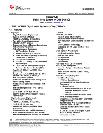
TMS320DM368SPRS668C – APRIL 2010 – REVISED JUNE 20111.3www.ti.comFunctional Block DiagramFigure 1-1 shows the functional block diagram of the TMS320DM368 device.16 BitISIFIPIPEResizerFace Det Lens DistVideo FESDTV/HDTVAnalog oOSDEncoderDigitalRGB/YUVDDR2Controller16 BitHPIVideo BEVPSS8/16 Bit16-BitDDR2/mDDRNAND/OneNAND/NOR Flash,SmartMedia/xDHost CPUDMA/Data and Configuration BusARM INTCHDVICPMJCPARM926EJ-SI-Cache RAM16 KB 32 KBD-Cache ROM8 KB 16 KBJTAGI/FCLOCK CtrlPLLPRTCSS19.2 MHz, 24 MHz 32.76827 MHz or 36 MHzkHzUSB2.0 HS w/OTGMMC/SD (x2)SPI (x5)UART (x2)I2CTimer (x4-64b)WDT (x1-64b)GIOPWM (x4)RTOMcBSPEMACADCKey ScanVoice CodecSystemI/OInterfacePMIC/SWFigure 1-1. Functional Block Diagram4TMS320DM368 Digital Media System-on-Chip (DMSoC)Copyright 2010–2011, Texas Instruments IncorporatedSubmit Documentation FeedbackProduct Folder Link(s): TMS320DM368
TMS320DM368SPRS668C – APRIL 2010 – REVISED JUNE 2011www.ti.com1TMS320DM368 Digital Media System-on-Chip(DMSoC) . 11.166.1Features . 1. 31.3Functional Block Diagram . 4Revision History (Revision C) . 62 Device Overview . 72.1Device Characteristics . 72.2Device Compatibility . 82.3ARM Subsystem Overview . 82.4System Control Module . 122.5Power Management . 132.6Memory Map Summary . 142.7Pin Assignments . 162.8Terminal Functions . 212.9Device Support . 463 Device Configurations . 503.1System Module Registers . 503.2Boot Modes . 513.3Device Clocking . 543.4Power and Sleep Controller (PSC) . 613.5Pin Multiplexing . 633.6Device Reset . 643.7Default Device Configurations . 643.8Debugging Considerations . 694 System Interconnect . 705 Device Operating Conditions . 711.2DescriptionRecommended Operating Conditions . 72Electrical Characteristics Over RecommendedRanges of Supply Voltageand Operating Case Temperature (UnlessOtherwise Noted) . 74. 76Recommended Clock and Control Signal TransitionBehavior . 776.3Power Supplies776.4Power-Supply te Maximum Ratings Over Operating CaseTemperature Range(Unless Otherwise Noted) . 717Parameter Information Device-Specific Information6.26.55.15.25.3Peripheral Information and ElectricalSpecifications . 76.Reset .Oscillators and Clocks .8081Power Management and Real Time ClockSubsystem (PRTCSS) . 85. 87. 89External Memory Interface (EMIF) . 99MMC/SD . 120General-Purpose Input/Output (GPIO)EDMA ControllerVideo Processing Subsystem (VPSS) Overview.123USB 2.0 . 147Universal Asynchronous Receiver/Transmitter(UART) . 155.6.17 Multi-Channel Buffered Serial Port (McBSP) .6.18 Timer .6.19 Pulse Width Modulator (PWM) .6.20 Real Time Out (RTO) .6.21 Ethernet Media Access Controller (EMAC) .6.22 Management Data Input/Output (MDIO) .6.23 Host-Port Interface (HPI) Peripheral .6.24 Key Scan .6.25 Analog-to-Digital Converter (ADC) .6.26 Voice Codec .6.27 IEEE 1149.1 JTAG .Mechanical Data .7.1Thermal Data for ZCE .7.2Packaging Information .6.15Serial Port Interface (SPI)1576.16Inter-Integrated Circuit (I2C)167ContentsCopyright 2010–2011, Texas Instruments IncorporatedSubmit Documentation FeedbackProduct Folder Link(s): 2045
TMS320DM368SPRS668C – APRIL 2010 – REVISED JUNE 2011www.ti.comRevision HistoryNOTE: Page numbers for previous revisions may differ from page numbers in the current version.highlights the technical changes made to the SPRS668B device-specific data sheet to make it aSPRS668C revision.Revision C UpdatesSeeGlobalRemoved sentence stating "micro-vias are not required."Figure 2-2Corrected J5 pin name.Table 2-5Changed TYPE of VREF pin from A I/O to A I.Table 2-5Changed TYPE of VCOM pin from AI to AO.Section 3.2.16Additions/Changes/DeletionsAdded 24 MHz reference clock to ARM ROM Boot - UART mode.Table 6-21Updated first table note.Table 6-22Updated second table note.Table 6-26Updated table and added table note.ContentsCopyright 2010–2011, Texas Instruments IncorporatedSubmit Documentation FeedbackProduct Folder Link(s): TMS320DM368
TMS320DM368SPRS668C – APRIL 2010 – REVISED JUNE 2011www.ti.com2 Device Overview2.1Device CharacteristicsTable 2-1 provides an overview of the DMSoC. The table shows significant features of the device,including the peripherals, capacity of on-chip RAM, ARM operating frequency, the package type with pincount, etc.Table 2-1. Characteristics of the ProcessorHARDWARE FEATURESDDR2 / mDDR Memory ControllerAsynchronous EMIF (AEMIF)Flash Card InterfacesPeripheralsAsynchronous (8/16-bit bus width) RAM,Flash (NOR, NAND, OneNAND)Two MMC/SDOne SmartMedia/xDEDMA64 independent DMA channelsEight QDMA channelsTimersFour 64-Bit General Purpose (eachconfigurable as two separate 32-bit timers)One 64-Bit Watch DogUARTTwo (one with RTS and CTS flow control)SPIFive (each supports two slave devices)I2COne (Master/Slave)Not all peripherals pins are10/100 Ethernet MAC with Management Data I/Oavailable at the same time (ForMulti-Channel Buffered Serial Port [McBSP]more detail, see the DeviceConfiguration section).Power Management and Real Time Clock Subsystem(PRTCSS)Key ScanOneOne McBSPRTC (32.768kHz), GPIO4 x 4 Matrix, 5 x 3 MatrixVoice CodecOneAnalog-to-Digital Converter (ADC)General-Purpose Input/Output PortPulse width modulator (PWM)Configurable Video Ports6-channel, 10-bit InterfaceUp to 104Four outputsOne Input (VPFE)One Output (VPBE)High Speed DeviceHigh Speed HostOn The Go (HS-USB-OTG)USB 2.0Wireless InterfacesThrough SDIORTOFour ChannelsARM16-KB I-cache, 8-KB D-cache, 32-KB RAM,16-KB ROMOn-Chip CPU MemoryOrganizationJTAG BSDL IDJTAGID register (address location: 0x01C4 0028)CPU Frequency (Maximum)MHzVoltageDEVICEDDR2 / mDDR (16-bit bus width)See Section 6.27.1, JTAG RegisterDescription(s)ARM: 432-MHzCore (V)1.35 VI/O (V)3.3 V, 1.8 VPLL OptionsReference frequency optionsConfigurable PLL controllerBGA Package13 x 13 mm19.2 MHz, 24 MHz, 27 MHz, 36 MHzPLL bypass, programmable PLL338-Pin BGA (ZCE)Process Technology65 nmDevice OverviewCopyright 2010–2011, Texas Instruments IncorporatedSubmit Documentation FeedbackProduct Folder Link(s): TMS320DM3687
TMS320DM368SPRS668C – APRIL 2010 – REVISED JUNE 2011www.ti.comTable 2-1. Characteristics of the Processor (continued)Product Status (1)(1)HARDWARE FEATURESDEVICEProduct Preview (PP),Advance Information (AI),or Production Data (PD)PDPRODUCTION DATA information is current as of publication date. Products conform to specifications per the terms of TexasInstruments standard warranty. Production processing does not necessarily include testing of all parameters.2.2Device CompatibilityThe ARM926EJ-S RISC CPU is compatible with other ARM9 CPUs from ARM Holdings plc.2.3ARM Subsystem OverviewThe ARM Subsystem contains components required to provide the ARM926EJ-S (ARM) master control ofthe overall device system, including the components of the ARM Subsystem, the peripherals, and theexternal memories.The ARM is responsible for handling system functions such as system-level initialization, configuration,user interface, user command execution, connectivity functions, interface and control of the subsystem,etc. The ARM is master and performs these functions because it has a large program memory space andfast context switching capability, and is thus suitable for complex, multi-tasking, and general-purposecontrol tasks.2.3.1Components of the ARM SubsystemThe ARM Subsystem consists of the following components: ARM926EJ-S RISC processor, including:– coprocessor 15 (CP15)– MMU– 16KB Instruction cache– 8KB Data cache– Write Buffer– Java accelerator ARM Internal Memories– 32KB Internal RAM (32-bit wide access)– 16KB Internal ROM (ARM bootloader for non-AEMIF boot modes) Embedded Trace Module and Embedded Trace Buffer (ETM/ETB) System Control Peripherals– ARM Interrupt Controller– PLL Controller– Power and Sleep Controller– System Control ModuleThe ARM also manages/controls all the device peripherals.Figure 2-1 shows the functional block diagram of the ARM Subsystem.8Device OverviewCopyright 2010–2011, Texas Instruments IncorporatedSubmit Documentation FeedbackProduct Folder Link(s): TMS320DM368
TMS320DM368SPRS668C – APRIL 2010 – REVISED JUNE )Master laveArbiter16K I CP158K D MMU16KROM16KRAM1PLLC2IF16KRAM0CFG BusDMA rals.Figure 2-1. ARM Subsystem Block Diagram2.3.2ARM926EJ-S RISC CPUThe ARM Subsystem integrates the ARM926EJ-S processor. The ARM926EJ-S processor is a member ofARM9 family of general-purpose microprocessors. This processor is targeted at multi-tasking applicationswhere full memory management, high performance, low die size, and low power are all important. TheARM926EJ-S processor supports the 32-bit ARM and 16 bit THUMB instruction sets, enabling the user totrade off between high performance and high code density. Specifically, the ARM926EJ-S processorsupports the ARMv5TEJ instruction set, which includes features for efficient execution of Java byte codes,providing Java performance similar to Just in Time (JIT) Java interpreter, but without associated codeoverhead.The ARM926EJ-S processor supports the ARM debug architecture and includes logic to assist in bothhardware and software debug. The ARM926EJ-S processor has a Harvard architecture and provides acomplete high performance subsystem, including: ARM926EJ -S integer core CP15 system control coprocessor Memory Management Unit (MMU) Separate instruction and data Caches Write buffer Separate instruction and data Tightly-Coupled Memories (TCMs) [internal RAM] interfaces Separate instruction and data AHB bus interfaces Embedded Trace Module and Embedded Trace Buffer (ETM/ETB)For more complete details on the ARM9, refer to the ARM926EJ-S Technical Reference Manual, availableat http://www.arm.comDevice OverviewCopyright 2010–2011, Texas Instruments IncorporatedSubmit Documentation FeedbackProduct Folder Link(s): TMS320DM3689
TMS320DM368SPRS668C – APRIL 2010 – REVISED JUNE 20112.3.3www.ti.comCP15The ARM926EJ-S system control coprocessor (CP15) is used to configure and control instruction anddata caches, Tightly-Coupled Memories (TCMs), Memory Management Unit (MMU), and other ARMsubsystem functions. The CP15 registers are programmed using the MRC and MCR ARM instructions,when the ARM in a privileged mode such as supervisor or system mode.2.3.4MMUThe ARM926EJ-S MMU provides virtual memory features required by operating systems such as Linux,WindowCE, ultron, ThreadX, etc. A single set of two level page tables stored in main memory is used tocontrol the address translation, permission checks and memory region attributes for both data andinstruction accesses. The MMU uses a single unified Translation Lookaside Buffer (TLB) to cache theinformation held in the page tables. The MMU features are: Standard ARM architecture v4 and v5 MMU mapping sizes, domains and access protection scheme. Mapping sizes are:– 1MB (sections)– 64KB (large pages)– 4KB (small pages)– 1KB (tiny pages) Access permissions for large pages and small pages can be specified separately for each quarter ofthe page (subpage permissions) Hardware page table walks Invalidate entire TLB, using CP15 register 8 Invalidate TLB entry, selected by MVA, using CP15 register 8 Lockdown of TLB entries, using CP15 register 102.3.5Caches and Write BufferThe size of the Instruction Cache is 16KB, Data cache is 8KB. Additionally, the Caches have the followingfeatures: Virtual index, virtual tag, and addressed using the Modified Virtual Address (MVA) Four-way set associative, with a cache line length of eight words per line (32-bytes per line) and withtwo dirty bits in the Dcache Dcache supports write-through and write-back (or copy back) cache operation, selected by memoryregion using the C and B bits in the MMU translation tables. Critical-word first cache refilling Cache lockdown registers enable control over which cache ways are used for allocation on a line fill,providing a mechanism for both lockdown, and controlling cache corruption Dcache stores the Physical Address TAG (PA TAG) corresponding to each Dcache entry in the TAGRAM for use during the cache line write-backs, in addition to the Virtual Address TAG stored in theTAG RAM. This means that the MMU is not involved in Dcache write-back operations, removing thepossibility of TLB misses related to the write-back address. Cache maintenance operations provide efficient invalidation of, the entire Dcache or Icache, regions ofthe Dcache or Icache, and regions of virtual memory.The write buffer is used for all writes to a noncachable bufferable region, write-through region and writemisses to a write-back region. A separate buffer is incorporated in the Dcache for holding write-back forcache line evictions or cleaning of dirty cache lines. The main write buffer has 16-word data buffer and afour-address buffer. The Dcache write-back has eight data word entries and a single address entry.2.3.6Tightly Coupled Memory (TCM)ARM internal RAM is provided for storing real-time and performance-critical code/data and the Interrupt10Device OverviewCopyright 2010–2011, Texas Instruments IncorporatedSubmit Documentation FeedbackProduct Folder Link(s): TMS320DM368
TMS320DM368SPRS668C – APRIL 2010 – REVISED JUNE 2011www.ti.comVector table. ARM internal ROM boot modes include NAND, MMC/SD, UART, USB, SPI, EMAC, and HPI.The RAM and ROM memories interfaced to the ARM926EJ-S via the tightly coupled memory interfacethat provides for separate instruction and data bus connections. Since the ARM TCM does not allowinstructions on the D-TCM bus or data on the I-TCM bus, an arbiter is included so that both data andinstructions can be stored in the internal RAM/ROM. The arbiter also allows accesses to the RAM/ROMfrom extra-ARM sources (e.g., EDMA or other masters). The ARM926EJ-S has built-in DMA support fordirect accesses to the ARM internal memory from a non-ARM master. Because of the time-critical natureof the TCM link to the ARM internal memory, all accesses from non-ARM devices are treated as DMAtransfers.Instruction and Data accesses are differentiated via accessing different memory map regions, with theinstruction region from 0x0000 through 0x7FFF and data from 0x10000 through 0x17FFF. Placing theinstruction region at 0x0000 is necessary to allow the ARM Interrupt Vector table to be placed at 0x0000,as required by the ARM architecture. The internal 32-KB RAM is split into two physical banks of 16KBeach, which allows simultaneous instruction and data accesses to be accomplished if the code and dataare in separate banks.2.3.7Advanced High-performance Bus (AHB)The ARM Subsystem uses the AHB port of the ARM926EJ-S to connect the ARM to the configuration busand the external memories. Arbiters are employed to arbitrate access to the separate D-AHB and I-AHBby the configuration bus and the external memories bus.2.3.8Embedded Trace Macrocell (ETM) and Embedded Trace Buffer (ETB)To support real-time trace, the ARM926EJ-S processor provides an interface to enable connection of anEmbedded Trace Macrocell (ETM). The ARM926ES-J Subsystem also includes the Embedded TraceBuffer (ETB). The ETM consists of two parts: Trace Port provides real-time trace capability for the ARM9. Triggering facilities provide trigger resources, which include address and data comparators, counter,and sequencers.The device trace port is not pinned out and is instead only connected to the Embedded Trace Buffer. TheETB has a 4KB buffer memory. ETB enabled debug tools are required to read/interpret the captured tracedata.2.3.9ARM Memory MappingThe ARM memory map is shown in Table 2-3 and Table 2-4. This section describes the memories andinterfaces within the ARM's memory map.2.3.9.1ARM Internal MemoriesThe ARM has access to the following ARM internal memories: 32KB ARM Internal RAM on TCM interface, logically separated into two 16KB pages to allowsimultaneous access on any given cycle if there are separate accesses for code (I-TCM bus) and data(D-TCM) to the different memory regions. 16KB ARM Internal ROM2.3.9.2External MemoriesThe ARM has access to the following External memories: DDR2 / mDDR Synchronous DRAM Asynchronous EMIF / OneNAND / NOR NAND FlashDevice OverviewCopyright 2010–2011, Texas Instruments IncorporatedSubmit Documentation FeedbackProduct Folder Link(s): TMS320DM36811
TMS320DM368SPRS668C – APRIL 2010 – REVISED JUNE 2011 www.ti.comFlash card devices:– MMC/SD– xD– SmartMedia2.3.10 PeripheralsThe ARM has access to all of the peripherals on the device.2.3.11 ARM Interrupt Controller (AINTC)The device ARM Interrupt Controller (AINTC) has the following features: Supports up to 64 interrupt channels (16 external channels) Interrupt mask for each channel Each interrupt channel can be mapped to a Fast Interrupt Request (FIQ) or to an Interrupt Request(IRQ) type of interrupt. Hardware prioritization of simultaneous interrupts Configurable interrupt priority (2 levels of FIQ and 6 levels of IRQ) Configurable interrupt entry table (FIQ and IRQ priority table entry) to reduce interrupt processing timeThe ARM core supports two interrupt types: FIQ and IRQ. See the ARM926EJ-S Technical ReferenceManual for detailed information about the ARM’s FIQ and IRQ interrupts. Each interrupt channel ismappable to an FIQ or to an IRQ type of interrupt, and each channel can be enabled or disabled. TheINTC supports user-configurable interrupt-priority and interrupt entry addresses. Entry addresses minimizethe time spent jumping to interrupt service routines (ISRs). When an interrupt occurs, the correspondinghighest priority ISR’s address is stored in the INTC’s ENTRY register. The IRQ or FIQ interrupt routine canread the ENTRY register and jump to the corresponding ISR directly. Thus, the ARM does not require asoftware dispatcher to determine the asserted interrupt.2.4System Control ModuleThe system control module is a system-level module containing status and top-level control logic requiredby the device. The system control module consists of a miscellaneous set of status and control registers,accessible by the ARM and supporting all of the following system features and operations: Device identification Device configuration– Pin multiplexing control– Device boot configuration status ARM interrupt and EDMA event multiplexing control Special peripheral status and control– Timer64– USB PHY control– VPSS clock and video DAC control and status– DDR VTP control– Clockout circuitry– GIO de-bounce control Power management– Deep sleep Bandwidth Management– Bus master DMA priority controlFor more information on the System Control Module refer to Section 3, Device Configurations and theTMS320DM36x DMSoC ARM Subsystem Reference Guide (literature number SPRUFG5).12Device OverviewCopyright 2010–2011, Texas Instruments IncorporatedSubmit Documentation FeedbackProduct Folder Link(s): TMS320DM368
TMS320DM368SPRS668C – APRIL 2010 – REVISED JUNE 2011www.ti.com2.5Power ManagementThe device is designed for minimal power consumption. There are two components to powerconsumption: active power and leakage power. Active power is the power consumed to perform work andscales with clock frequency and the amount of computations being performed. Active power can bereduced by controlling the clocks in such a way as to either operate at a clock setting just high enough tocomplete the required operation in the required time-line or to run at a clock setting until the work iscomplete and then drastically cut the clocks (e.g. to PLL Bypass mode) until additional work must beperformed. Leakage power is due to static current leakage and occurs regardless of the clock rate.Leakage, or standby power, is unavoidable while power is applied and scales roughly with the operatingjunction temperatures. Leakage power can o
www.ti.com SPRS668C-APRIL 2010-REVISED JUNE 2011 TMS320DM368 Digital Media System-on-Chip(DMSoC) Check for Samples: TMS320DM368 1 TMS320DM368 Digital Media System-on-Chip(DMSoC) . 10/100 Mb/s Ethernet Media Access Controller -Time Division Multiplexed Mode (TDM) (EMAC) -Digital Media -128 Channel Mode -IEEE 802.3 Compliant .