Transcription
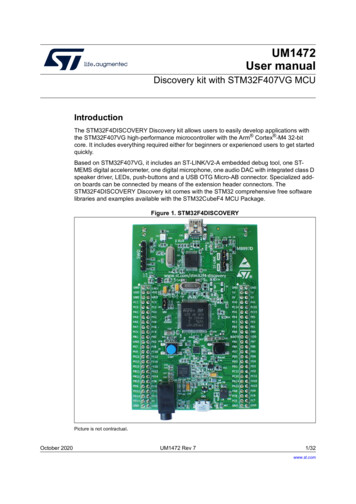
UM1775User manualDiscovery kit with STM32L053C8 MCUIntroductionThe STM32L053 Discovery kit (32L0358DISCOVERY) helps the user to discover the fullfeature range of the STM32L0 Series and develop applications. It is based on theSTM32L053C8T6 microcontroller and includes an embedded ST-LINK/V2-1debugger/programmer, linear touch sensor, touchkeys, IDD current measurement, 2.13” Epaper display, NFC connector for the PLUG-CR95HF-B board, LEDs, push-buttons and aUSB Mini-B connector.The STM32L053 Discovery kit comes with a comprehensive STM32 software HAL librarywith various packaged software examples available in the STM32CubeL0 MCU Package.Figure 1. STM32L053 Discovery boardPicture is not contractual.February 2022UM1775 Rev 61/39www.st.com
ContentsUM1775Contents1Features . . . . . . . . . . . . . . . . . . . . . . . . . . . . . . . . . . . . . . . . . . . . . . . . . . . 62Ordering information . . . . . . . . . . . . . . . . . . . . . . . . . . . . . . . . . . . . . . . . 72.13Codification . . . . . . . . . . . . . . . . . . . . . . . . . . . . . . . . . . . . . . . . . . . . . . . . . 7Development environment . . . . . . . . . . . . . . . . . . . . . . . . . . . . . . . . . . . . 83.1System requirements . . . . . . . . . . . . . . . . . . . . . . . . . . . . . . . . . . . . . . . . . 83.2Development toolchains . . . . . . . . . . . . . . . . . . . . . . . . . . . . . . . . . . . . . . . 84Conventions . . . . . . . . . . . . . . . . . . . . . . . . . . . . . . . . . . . . . . . . . . . . . . . . 85Quick start . . . . . . . . . . . . . . . . . . . . . . . . . . . . . . . . . . . . . . . . . . . . . . . . . 95.16Hardware layout . . . . . . . . . . . . . . . . . . . . . . . . . . . . . . . . . . . . . . . . . . . 106.16.22/39Getting started . . . . . . . . . . . . . . . . . . . . . . . . . . . . . . . . . . . . . . . . . . . . . . 9Embedded ST-LINK/V2-1 . . . . . . . . . . . . . . . . . . . . . . . . . . . . . . . . . . . . . 136.1.1Drivers . . . . . . . . . . . . . . . . . . . . . . . . . . . . . . . . . . . . . . . . . . . . . . . . . . 136.1.2ST-LINK/V2-1 firmware upgrade . . . . . . . . . . . . . . . . . . . . . . . . . . . . . . 146.1.3VCP configuration . . . . . . . . . . . . . . . . . . . . . . . . . . . . . . . . . . . . . . . . . 146.1.4Using ST-LINK/V2-1 to program/debug the STM32L053C8T6 on board .156.1.5Using ST-LINK/V2-1 to program/debug an externalSTM32 application . . . . . . . . . . . . . . . . . . . . . . . . . . . . . . . . . . . . . . . . . 16Power supply and power selection . . . . . . . . . . . . . . . . . . . . . . . . . . . . . . 176.2.1Power supply input from the USB connector . . . . . . . . . . . . . . . . . . . . . 186.2.2External power supply inputs: 5V IN or USB USER CN3 . . . . . . . . . . . 196.3LEDs . . . . . . . . . . . . . . . . . . . . . . . . . . . . . . . . . . . . . . . . . . . . . . . . . . . . 196.4Pushbuttons . . . . . . . . . . . . . . . . . . . . . . . . . . . . . . . . . . . . . . . . . . . . . . . 196.5NFC connector for PLUG-CR95HF-B board . . . . . . . . . . . . . . . . . . . . . . 206.6Electronic paper display (EPD) . . . . . . . . . . . . . . . . . . . . . . . . . . . . . . . . 216.7JP4 (IDD) . . . . . . . . . . . . . . . . . . . . . . . . . . . . . . . . . . . . . . . . . . . . . . . . . . 216.8BOOT0 configuration . . . . . . . . . . . . . . . . . . . . . . . . . . . . . . . . . . . . . . . . 226.9Linear touch sensor / touchkeys . . . . . . . . . . . . . . . . . . . . . . . . . . . . . . . . 226.10USB device support . . . . . . . . . . . . . . . . . . . . . . . . . . . . . . . . . . . . . . . . . 23UM1775 Rev 6
UM1775Contents6.11USART configuration . . . . . . . . . . . . . . . . . . . . . . . . . . . . . . . . . . . . . . . . 236.12OSC clock supply . . . . . . . . . . . . . . . . . . . . . . . . . . . . . . . . . . . . . . . . . . . 236.13OSC 32 KHz clock supply . . . . . . . . . . . . . . . . . . . . . . . . . . . . . . . . . . . . 246.14Solder bridges . . . . . . . . . . . . . . . . . . . . . . . . . . . . . . . . . . . . . . . . . . . . . 256.15Extension connectors . . . . . . . . . . . . . . . . . . . . . . . . . . . . . . . . . . . . . . . . 267Mechanical drawing . . . . . . . . . . . . . . . . . . . . . . . . . . . . . . . . . . . . . . . . 32832L0358DISCOVERY Discovery kit information . . . . . . . . . . . . . . . . . . 338.1Product marking . . . . . . . . . . . . . . . . . . . . . . . . . . . . . . . . . . . . . . . . . . . . 338.232L0358DISCOVERY product history . . . . . . . . . . . . . . . . . . . . . . . . . . . 348.38.49Product identification 32L0538DISCO/ . . . . . . . . . . . . . . . . . . . . . . . . . 348.2.2Product identification DK32L0538 AU1 . . . . . . . . . . . . . . . . . . . . . . . . 34Board revision history . . . . . . . . . . . . . . . . . . . . . . . . . . . . . . . . . . . . . . . . 348.3.1MB1143 revision B-01 . . . . . . . . . . . . . . . . . . . . . . . . . . . . . . . . . . . . . . 348.3.2MB1143 revision B-03 . . . . . . . . . . . . . . . . . . . . . . . . . . . . . . . . . . . . . . 34Board known limitations . . . . . . . . . . . . . . . . . . . . . . . . . . . . . . . . . . . . . . 348.4.1MB1143 revision B-01 . . . . . . . . . . . . . . . . . . . . . . . . . . . . . . . . . . . . . . 348.4.2MB1143 revision B-03 . . . . . . . . . . . . . . . . . . . . . . . . . . . . . . . . . . . . . . 34Federal Communications Commission (FCC)and ISED Canada Compliance Statements . . . . . . . . . . . . . . . . . . . . . . 359.19.2108.2.1FCC Compliance Statement . . . . . . . . . . . . . . . . . . . . . . . . . . . . . . . . . . . 359.1.1Part 15.19 . . . . . . . . . . . . . . . . . . . . . . . . . . . . . . . . . . . . . . . . . . . . . . . 359.1.2Part 15.21 . . . . . . . . . . . . . . . . . . . . . . . . . . . . . . . . . . . . . . . . . . . . . . . 359.1.3Part 15.105 . . . . . . . . . . . . . . . . . . . . . . . . . . . . . . . . . . . . . . . . . . . . . . 35ISED Compliance Statement . . . . . . . . . . . . . . . . . . . . . . . . . . . . . . . . . . 36CE conformity . . . . . . . . . . . . . . . . . . . . . . . . . . . . . . . . . . . . . . . . . . . . . 37Revision history . . . . . . . . . . . . . . . . . . . . . . . . . . . . . . . . . . . . . . . . . . . . . . . . . . . . 38UM1775 Rev 63/393
List of tablesUM1775List of tablesTable 1.Table 2.Table 3.Table 4.Table 5.Table 6.Table 7.Table 8.Table 9.4/39Ordering information . . . . . . . . . . . . . . . . . . . . . . . . . . . . . . . . . . . . . . . . . . . . . . . . . . . . . . . 7Codification explanation . . . . . . . . . . . . . . . . . . . . . . . . . . . . . . . . . . . . . . . . . . . . . . . . . . . . 7ON/OFF conventions . . . . . . . . . . . . . . . . . . . . . . . . . . . . . . . . . . . . . . . . . . . . . . . . . . . . . . 8Jumper states . . . . . . . . . . . . . . . . . . . . . . . . . . . . . . . . . . . . . . . . . . . . . . . . . . . . . . . . . . . 13Debug connector CN5 (SWD) . . . . . . . . . . . . . . . . . . . . . . . . . . . . . . . . . . . . . . . . . . . . . . 16NFC connector pinout . . . . . . . . . . . . . . . . . . . . . . . . . . . . . . . . . . . . . . . . . . . . . . . . . . . . . 21Solder bridges. . . . . . . . . . . . . . . . . . . . . . . . . . . . . . . . . . . . . . . . . . . . . . . . . . . . . . . . . . . 25Extension connectors . . . . . . . . . . . . . . . . . . . . . . . . . . . . . . . . . . . . . . . . . . . . . . . . . . . . . 26Document revision history . . . . . . . . . . . . . . . . . . . . . . . . . . . . . . . . . . . . . . . . . . . . . . . . . 38UM1775 Rev 6
UM1775List of figuresList of figuresFigure 1.Figure 2.Figure 3.Figure 4.Figure 5.Figure 6.Figure 7.Figure 8.Figure 9.Figure 10.Figure 11.Figure 12.STM32L053 Discovery board . . . . . . . . . . . . . . . . . . . . . . . . . . . . . . . . . . . . . . . . . . . . . . . . 1STM32L053 Discovery board hardware block diagram . . . . . . . . . . . . . . . . . . . . . . . . . . . 10Top layout . . . . . . . . . . . . . . . . . . . . . . . . . . . . . . . . . . . . . . . . . . . . . . . . . . . . . . . . . . . . . . 11Bottom layout . . . . . . . . . . . . . . . . . . . . . . . . . . . . . . . . . . . . . . . . . . . . . . . . . . . . . . . . . . . 12Updating the list of drivers in device manager . . . . . . . . . . . . . . . . . . . . . . . . . . . . . . . . . . 13STM32L053 Discovery board connections . . . . . . . . . . . . . . . . . . . . . . . . . . . . . . . . . . . . . 15ST-LINK/V2-1 connections . . . . . . . . . . . . . . . . . . . . . . . . . . . . . . . . . . . . . . . . . . . . . . . . . 17NFC board plugged on the STM32L053 Discovery board . . . . . . . . . . . . . . . . . . . . . . . . . 20Jumper JP4 in position OFF . . . . . . . . . . . . . . . . . . . . . . . . . . . . . . . . . . . . . . . . . . . . . . . . 21Jumper JP4 in position ON (default) . . . . . . . . . . . . . . . . . . . . . . . . . . . . . . . . . . . . . . . . . . 22No Jumper on JP4 . . . . . . . . . . . . . . . . . . . . . . . . . . . . . . . . . . . . . . . . . . . . . . . . . . . . . . . 22STM32L053 Discovery board mechanical drawing. . . . . . . . . . . . . . . . . . . . . . . . . . . . . . . 32UM1775 Rev 65/395
Features1UM1775FeaturesThe STM32L053 Discovery kit offers the following features: STM32L053C8T6 microcontroller, based on the Arm (a) Cortex -M0 processor, with64 Kbytes of flash memory and 8 Kbytes of RAM, in an LQFP48 package 2.13" E-paper display, 122 250 pixels USB 2.0 FS One linear touch sensor or four touchkeys Reset and user push-buttons Four LEDs:–LD1 (red/green) for USB communication–LD2 (red) for 3.3 V power on–Two user LEDs: LD3 (green), LD4 (red) IDD current measurement Board connectors:–USB Mini-B connector–NFC expansion connector for the PLUG-CR95HF-B daughterboard–2.54 mm pitch expansion header for direct access to various features of theSTM32L053C8T6 microcontroller and easy probing of the LQFP48 I/Os Flexible power-supply options: ST-LINK USB VBUS, USB connector, or externalsources External application power supply: 3 V and 5 V Comprehensive free software libraries and examples available with the STM32CubeL0MCU Package On-board ST-LINK/V2-1 debugger/programmer with USB re-enumeration capability:mass storage, Virtual COM port, and debug port Support of a wide choice of Integrated Development Environments (IDEs) includingIAR Embedded Workbench , MDK-ARM, and STM32CubeIDEa. Arm is a registered trademark of Arm Limited (or its subsidiaries) in the US and/or elsewhere.6/39UM1775 Rev 6
UM17752Ordering informationOrdering informationTo order the 32L0358DISCOVERY Discovery kit, refer to Table 1. Additional information isavailable from the datasheet and reference manual of the target microcontroller.Table 1. Ordering information2.1Order codeBoard referenceTarget onThe meaning of the codification is explained in Table 2.Table 2. Codification ionExample: STM32L0538-DISCOMCU series in STM32 32-bit Arm CortexSTM32L0 SeriesMCUsMCU product line in the seriesSTM32L0x3 includes theSTM32L053xx MCUsSTM32 flash memory size:– 8 for 64 Kbytes64 KbytesDiscovery kitDiscovery kitUM1775 Rev 67/3938
Development environmentUM17753Development environment3.1System requirements3.24 Multi.OS support: Windows 10, Linux (a) 64-bit, or macOS (b) USB Type-A or USB Type-C to Mini-B cableDevelopment toolchains IAR Systems - IAR Embedded Workbench (c) Keil - MDK-ARM(c) (d) (e) STMicroelectronics - STM32CubeIDEConventionsTable 3 provides the definition of some conventions used in the present document.Table 3. ON/OFF conventionsConventionDefinitionJumper JPx ONJumper fittedJumper JPx OFFJumper not fittedSolder bridge SBx ONSBx connections closed by solderSolder bridge SBx OFFSBx connections left opena. Linux is a registered trademark of Linus Torvalds.b. macOS is a trademark of Apple Inc. registered in the U.S. and other countries.All other trademarks are the property of their respective owners.c.On Windows only.d. Free MDK-ARM for Arm Cortex -M0/M0 cores.e. All other trademarks are the property of their respective owners.8/39UM1775 Rev 6
UM17755Quick startQuick startThe STM32L053 Discovery kit is a low-cost and easy-to-use development kit to quicklyevaluate and start a development with the STM32L053C8T6 ultra-low-power microcontrollerin the STM32L0 Series.Before installing and using the product, accept the Evaluation Product License Agreementfrom the www.st.com/stm32l0-discovery webpage.For more information on the STM32L053 Discovery kit, visit the www.st.com/stm32l0discovery webpage.5.1Getting startedRefer to the sequence of operations described on the product packaging.UM1775 Rev 69/3938
Hardware layout6UM1775Hardware layoutThe STM32L053 Discovery board is designed around the STM32L053C8T6 microcontrollerin a 48-pin LQFP package.Figure 2 illustrates the connections between the STM32L053C8T6 and its peripherals (STLINK/V2-1, linear touch sensor, touchkeys, IDD current measurement, 2.13” E-paperdisplay, NFC connector for PLUG-CR95HF-B board, LEDs, push-buttons and an USB MiniB connector).Figure 3 and Figure 4 help users to locate these features on the STM32L053 Discoveryboard.Figure 2. STM32L053 Discovery board hardware block diagramUSB ST-LINKMini-BUSB /ORESETLEDsLD3, LD4B2RESETLineartouch sensorB1USERHeaderI/OHeaderI/OIDD currentmeasurementNFCconnectorE-paper displayMSv39739V210/39UM1775 Rev 6
UM1775Hardware layoutFigure 3. Top layoutST-LINK/V2-1COM(LD1)USB ST-LINKUSB USERPWR(LD2)NFC SCOVERYselector (CN4)RX,TX(JP3)VCP RX, TX(SB2, SB3)5 V powersupply input3 V powersupply output5 V powersupply outputConfiguration(BOOT0)IDD measurement(JP4)2.13" E-paper display(U4)Green LED(LD3)Red LED(LD4)Reset button(B2)User button(B1)Linear touch sensor/TouchkeysMSv34155V3UM1775 Rev 611/3938
Hardware layoutUM1775Figure 4. Bottom layoutReserved(SB4, 5, 6, 11)Default(SB7,8,9,12)STM RST(SB10)NRST(SB13)RX, TX(SB14,15)X2 crystal(SB18,19)Crystal(X2)USB USER(SB16, 17)MCO(SB20)STM32L053C8T6(U8)OSC IN(SB21)B2 – RESET(SB29)B1 – USER(SB22)Touch sensor(SB23, 24, 25, 26, 27, 28)MSv34156V312/39UM1775 Rev 6
UM17756.1Hardware layoutEmbedded ST-LINK/V2-1The ST-LINK/V2-1 programming and debugging tool is integrated on the STM32L053Discovery board.The embedded ST-LINK/V2-1 supports only SWD for STM32 devices.For information about the debugging and programming features, refer to the ST-LINK/V2 incircuit debugger/programmer for STM8 and STM32 user manual (UM1075). For acomparison of the various ST-LINK solutions, refer to the Overview of ST-LINK derivativestechnical note (TN1235).There are two different ways to use the embedded ST-LINK/V2-1 depending on the jumperstates (see Table 4): program/debug the MCU on board (Section 6.1.4). program/debug an MCU in an external application board using a cable connected toSWD connector CN5 (Section 6.1.5).Table 4. Jumper statesJumper stateBoth CN4 jumpers ONBoth CN4 jumpers OFF6.1.1DescriptionST-LINK/V2-1 functions enabled for on board programming (default)ST-LINK/V2-1 functions enabled for application through external CN5connector (SWD supported)DriversST-LINK/V2-1 requires a dedicated USB driver, which, for Windows 7, Windows 8 andWindows 10, is available from www.st.com.In cases where the STM32L053 Discovery board is connected to the PC before the driver isinstalled, some STM32L053 Discovery board interfaces might be declared as “Unknown” inthe PC device manager. In such cases, the user must install the dedicated driver files andupdate the driver of the connected device from the device manager, as shown in Figure 5.Note:It is preferable to use the “USB Composite Device” handle for a full recovery.Figure 5. Updating the list of drivers in device managerUM1775 Rev 613/3938
Hardware layout6.1.2UM1775ST-LINK/V2-1 firmware upgradeST-LINK/V2-1 embeds a mechanism for in-situ firmware upgrade through the USB port. Asfirmware may evolve during the lifespan of the ST-LINK/V2-1 product (for example newfunctionalities, bug fixes, support for new microcontroller families), visiting the www.st.comwebsite is recommended before starting to use the STM32L053 Discovery board, thenperiodically to stay up-to-date with the latest firmware version.6.1.3VCP configurationST-LINK/V2-1 supports the Virtual COM port (VCP). To enable this function, the solderbridges SB2 and SB3 are closed (See Figure 3: Top layout). Table 7: Solder bridgesindicates this with the ON state.14/39UM1775 Rev 6
UM17756.1.4Hardware layoutUsing ST-LINK/V2-1 to program/debug the STM32L053C8T6 on boardTo program the STM32L053C8T6 on board, simply plug in the two jumpers on CN4, asshown in Figure 6 in pink, but do not use the CN5 connector as that could disturb thecommunication with the STM32L053C8T6 of the STM32L053 Discovery board.Figure 6. STM32L053 Discovery board connectionsUM1775 Rev 615/3938
Hardware layout6.1.5UM1775Using ST-LINK/V2-1 to program/debug an externalSTM32 applicationIt is very easy to use ST-LINK/V2-1 to program an STM32 microcontroller on an externalapplication. Simply remove the two jumpers from CN4 as shown in Figure 7 and connect theapplication to the CN5 debug connector according to Table 5.Note:SB13, must be OFF if CN5 pin 5 (NRST) is used in the external application.Table 5. Debug connector CN5 (SWD)Pïn16/39CN5Designation1VDD TARGETVDD from application2SWLCKSWD clock3GNDGround4SWDIOSWD data input/output5NRSTRESET of target MCU6SWOReservedUM1775 Rev 6
UM1775Hardware layoutFigure 7. ST-LINK/V2-1 connections6.2Power supply and power selectionThe power supply is provided either by the host PC through the USB cable, or by anexternal 5 V power supply.The STM32L053 Discovery board requires 300 mA from the host PC: about 90 mA areneeded by a simple E-paper demo application, 100 mA for an extension board, and 100 mAas a safety margin.UM1775 Rev 617/3938
Hardware layoutUM1775The D3, D4 and D6 diodes protect the 5 V pins from external power supplies:6.2.1 5 V and 3 V can be used as output power supplies when an extension board isconnected to pins P2 and P3.In this case, the 5V O and 3V O pins deliver a 5 V or 3.3 V power supply and thepower consumption of the extension board must be lower than 100 mA. 5 V can also be used as input power supply, for instance when the USB connector isnot connected to the PC (pin 5V I of header P3).In this case, the STM32L053 Discovery board must be powered by a power supply unitor by an auxiliary equipment complying with standard EN-60950-1: 2006 A11/2009. Itmust be Safety Extra Low Voltage (SELV) with limited power capability.Power supply input from the USB connectorST-LINK/V2-1 supports USB power management allowing the request of more than 100 mAfrom the host PC.All parts of the STM32L053 Discovery board and extension board can be powered from theST-LINK/V2-1 USB connector CN2 (U5V or VBUS). Note that only the ST-LINK/V2-1 part ispower supplied before the USB enumeration as the host PC only provides 100 mA to theboard at that time. During the USB enumeration, the STM32L053 Discovery board requires300 mA from the host PC. If the host is able to provide the required power, the target STM32 microcontroller ispowered and the red LED LD2 is turned ON. The STM32L053 Discovery board and itsextension board can consume not more than a maximum of 300 mA. If the host is not able to provide the required current, the target STM32 microcontrollerand the MCU part including the extension board are not power supplied. As aconsequence the red LED LD2 remains turned OFF. In such a case, it is mandatory touse an external power supply as explained in the next section.Warning: If the maximum current consumption of the STM32L053 Discovery board and itsextension board exceeds 300 mA, it is mandatory to power the STM32L053 Discoveryboard with an external power supply connected to 5V IN.Note:18/39In cases where this board is powered by a USB charger or USB battery, there is no USBenumeration. Therefore, LED LD1 remains OFF permanently and the target MCU is notpowered. In this specific case, the jumper JP2 must be ON to allow the target MCU to bepowered anyway. This is a special use case without enumeration and JP2 is not soldered.To use this optional power supply, solder a 2-pin header in JP2 and set a jumper.UM1775 Rev 6
UM17756.2.2Hardware layoutExternal power supply inputs: 5V IN or USB USER CN3The external power source 5V IN or USB USER CN3 is automatically detected. In this casethe current consumption of the STM32L053 Discovery board and its extension board mayexceed the allowed current on the USB. In this condition it is still possible to use the USB forcommunication, for programming or debugging only, but it is mandatory to power supply theboard first using 5V IN or USB USER CN3 then connecting the USB cable to the PC.Proceeding this way ensures that the enumeration occurs with the support of the externalpower source.The following power sequence procedure must be respected:1.Connect the external power source to 5V IN or USB USER CN3.2.Power on the external power supply 5V IN or USB USER CN3.3.Check that LD2 is turned on.4.Connect the PC to USB connector CN2.If this order is not respected, the board may be supplied by VBUS first, then by 5V IN or USBUSER CN3. Consequently, the following risks may be encountered:6.36.41.If more than 300 mA is needed by the board, the PC may be damaged or the currentsupply can be limited by the PC. As a consequence the board is not powered correctly.2.300 mA is requested at enumeration (since JP2 must be OFF) so there is a risk that therequest is rejected and the enumeration does not succeed if the PC cannot providesuch current. Consequently the board is not power supplied (LED LD2 remains OFF).LEDs LD1 COM:LD1 default status is red. LD1 turns to green to indicate that communication is inprogress between the PC and ST-LINK/V2-1. LD2 PWR:The red LED indicates that the board is powered. User LD3:The green LED is a user LED connected to the I/O PB4 of the STM32L053C8T6. User LD4:The red LED is a user LED connected to the I/O PA5 of the STM32L053C8T6.Pushbuttons B1 USER:User and Wake-Up button connected to the I/O PA0 of the STM32L053C8T6. B2 RESET:The pushbutton connected to NRST is used to RESET the STM32L053C8T6.UM1775 Rev 619/3938
Hardware layout6.5UM1775NFC connector for PLUG-CR95HF-B boardA NFC (Near Field Communication) transceiver board can be connected to the STM32L053Discovery board, for example the PLUG-CR95HF-B board.The NFC board is plugged in connector CN1 of STM32L053 Discovery board as following:Figure 8. NFC board plugged on the STM32L053 Discovery board20/39UM1775 Rev 6
UM1775Hardware layoutThe NFC board can be accessed in the SPI or UART mode.Table 6. NFC connector pinoutCN1 pin6.6NFC signalsSTM32L053C8T6Description1NFC IRQOUTNor UART1 TXPB7Interrupt output for NFC connected toSTM32L053C8T6 UART1 RX2NFC IRQINN orUART1 RXPB6Interrupt input for CR95HF connected toSTM32L053C8T6 UART1 TX3NFC NSSPB12SPI slave select4NFC MISOPB14SPI data, slave output5NFC MOSIPB15SPI data, slave input6NFC SCKPB13SPI serial clock7 3V3-Main power supply/power supply for RF drivers8GND-GroundElectronic paper display (EPD)The STM32L053 Discovery board includes an E-paper display with high contrast, highreflectance and ultra-wide viewing angle.This display is a TFT active matrix electrophoretic display. The 2.13" active area contains122 250 pixels and it is capable to display images at 1-bit white, black full displaycapabilities. An associated integrated circuit contains the buffers, interface, control logic,oscillator, and DC-DC converter.The STM32L053C8T6 controls this peripheral and is able to switch off its power supply.6.7JP4 (IDD)Jumper JP4, labeled Idd, allows STM32L053C8T6 consumption direct measurement by amodule on board able to measure from 100 nA to 50 mA or by removing the jumper andconnecting an ammeter. Jumper in position OFF: STM32L053C8T6 is powered.Figure 9. Jumper JP4 in position OFFUM1775 Rev 621/3938
Hardware layout UM1775Jumper in position ON (default): a module onboard is designed to measure from100 nA to 50 mA by using several MOSFET and switching automatically depending onthe read value.Figure 10. Jumper JP4 in position ON (default) NO Jumper on JP4: an ammeter must be connected to measure the STM32L053C8T6current through pins 1 and 2 (if there is no ammeter, the STM32L053C8T6 is notpowered).Figure 11. No Jumper on JP46.8BOOT0 configurationBOOT0 is at level “0” through a pull-down R65. To set BOOT0 at level “1”, use aconfiguration with a jumper between P2.6 (BOOT0) and P2.5 (VDD).Note:To set BOOT0 at level "1" continuously, prefer to unsolder the resistor R65 to avoid aconsumption of 6 mA while connecting pin P2.6 (BOOT0) and P2.5 (VDD) with a jumper ora wire.6.9Linear touch sensor / touchkeysTo demonstrate touch sensing capabilities, the STM32L053 Discovery board includes alinear touch sensor, which can be used either as a three-position linear touch sensor or asfour touchkeys.Three pairs of I/O ports are assigned to the linear touch sensor / touchkeys. Each pair mustbelong to the same analog switch group:22/39 PA2, PA3 (group 1) PA6, PA7 (group 2) PB0, PB1 (group 3)UM1775 Rev 6
UM1775Hardware layoutTo minimize the noise, these pairs are dedicated to the linear touch sensor and touchkeys.They are not connected to external headers. To design a touch sensing application, refer tothe following documentation and firmware: For details concerning the I/O ports, refer to the STM32L053C8T6 datasheet. For more detail concerning touch sensing application design and layout, refer to theapplication note Design with surface sensors for touch sensing applications on MCUs(AN4312). STM32 touch sensing library available from www.st.com/stm32l0-discovery.The STM32L053C8T6 MCU controls the linear touch sensor and the touchkeys.6.10USB device supportThe STM32L053C8T6 MCU is also used to drive the second USB Mini-B connector (USBUSER), which allows the use of the board as a USB Device. The STM32L053 Discoveryboard can then act as a USB joystick, mouse, or other similar device. If both USBs areconnected, diodes D3 and D4 protect the board and use the power from USB ST-LINK orUSB USER (see Section 6.2.2: External power supply inputs: 5V IN or USB USER CN3).The board can be powered through this USB USER connector, in which case LED2 PWRlights up, LED1 COM blinks and it can run an application in standalone mode.The STM32L053C8T6 MCU controls the USB USER through PA11 and PA12.6.11USART configurationThe USART1 interface available on PA9 and PA10 of the STM32L053C8T6 can beconnected to the ST-LINK/V2-1 MCU to use the Virtual COM port function.By default, the USART1 communication between the target STM32L053C8T6 and theST-LINK/V2-1 MCU is not enabled.To use the Virtual COM port function with:6.12 The on-board STM32L053C8T6, set SB2 and SB3 ON. (SB14,15 must be OFF) An external MCU, remove solder from SB2 and SB3, solder a 2-pin header on JP3,then connect RX and TX of the external MCU directly to RX and TX of JP3OSC clock supplyIf PH0 is only used as GPIO instead of as a clock, then SB21 is ON. (SB20 must be OFF)MCO from ST-LINK/V2-1 (from MCO of the STM32L053C8T6)This frequency cannot be changed, it is fixed at 8 MHz and connected to PH0-OSC IN ofthe STM32L053C8T6. The configuration needed is:–SB20 ON and SB21 OFFOscillator from external PH0 (from external oscillator through pin 7 of the P3 connector)The configuration needed is:–Note:SB21 ON and SB20 OFFRefer to application note AN2867 for STM32 microcontrollers oscillator design guide.UM1775 Rev 623/3938
Hardware layout6.13UM1775OSC 32 KHz clock supplyIf PC14 and PC15 are only used as GPIOs instead of as a clock, then SB18 and SB19 areON and R70 and R71 are removed.HSE oscillator onboard from X2 crystal (not provided)For typical frequencies and its capacitors and resistors, please refer to the STM32L053C8T6Datasheet. The configuration needed is:–SB18, SB19 OFF–X2, R70, R71, C47, C50 solderedOscillator from external PC14 (from external oscillator through pin 5 of the P3 connector)the configuration needed is:Note:24/39–SB18 ON–SB19 OFF–R70 removedRefer to application note AN2867 for STM32 microcontrollers oscillator design guide.UM1775 Rev 6
UM17756.14Hardware layoutSolder bridgesTable 7. Solder bridgesBridge(1)StateDescriptionOFFX2, C47, C50, R70 and R71 provide a clock. PC14, PC15 are disconnectedfrom P3.ONPC14, PC15 are connected from P3. Remove only R70 and R71SB7,8,9,12 (default)ONReserved, do not modifySB4,5,6,11 (reserved)OFFReserved, do not modifySB14,15 (reserved)OFFReserved, do not modifyONB2 Push Button is connected to NRST of STM32L053C8T6OFFB2 Push Button is not connected to NRST of STM32L053C8T6ONB1 Push Button is connected to PA0OFFB1 Push Button is not connected to PA0OFFPA2, PA3 of STM32F103CBT6 are not connected to PA10, PA9 ofSTM32L053C8T6ONPA2, PA3 of STM32F103CBT6 are connected to PA10, PA9 ofSTM32L053C8T6OFFUSB1 DP and USB1 DM are dedicated to the USB USER connector CN3ONUSB1 DP is connected to PA12 and USB1 DM is connected to PA11. Both areavailable as GPIO on P2, P3 headers.SB23,24,25,26,27,28(touch sensor)OFFPA2, PA3, PA6, PA7, PB0, PB1 are dedicated to touch sensor.ONPA2, PA3, PA6, PA7, PB0, PB1 are available as GPIO on P2, P3 headers.SB1 (ST-LINK/V2-1PWR)ONST-LINK/V2-1 module is poweredOFFST-LINK/V2-1 module is not poweredOFFClock signal from header P3.7 is connected to OSC IN of STM32L053C8T6 orPH0 is available as GPIO. SB20 must be OFFONNo connection between header P3.7 and PH0 of STM32L053C8T6ONT NRST signal from connector CN5 and STM32F103CBT6, is connected toNRST of STM32L053C8T6OFFT NRST signal is not connectedOFFNo incidence on NRST signal of STM32F103CBT6ONNRST signal of STM32F103CBT6 is connected to GNDONMCO clock signal from STM32F103CBT6 is
STM32L0538-DISCO MB1143 STM32L053C8T6 STM32L0XXY-DISCO Description Example: STM32L0538-DISCO STM32L0 MCU series in STM32 32-bit Arm Cortex MCUs STM32L0 Series XX MCU product line in the series STM32L0x3 includes the STM32L053xx MCUs Y STM32 flash memory size: - 8 for 64 Kbytes 64 Kbytes DISCO Discovery kit Discovery kit