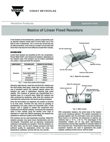
Transcription
VEML7700www.vishay.comVishay SemiconductorsHigh Accuracy Ambient Light Sensor With I2C InterfaceFEATURES Package type: surface-mount Package: side view Dimensions (L x W x H in mm): 6.8 x 2.35 x 3.0 Integrated modules: ambient light sensor (ALS) Supply voltage range VDD: 2.5 V to 3.6 V Communication via I2C interface Floor life: 72 h, MSL 4, according to J-STD-0204 Low shut down current consumption: typ. 0.5 μA3 Material categorization: for definitions of complianceplease see www.vishay.com/doc?9991221AMBIENT LIGHT FUNCTIONPinning FiltronTM technology adaption: close to real human eyeresponse1: SCL O-TrimTM technology adoption: ALS output tolerance 10 %2: VDD3: GND 16-bit dynamic range for ambient light detection from0 lx to about 120 klx with resolution down to 0.0036 lx/ct,supports low transmittance (dark) lens design4: SDADESCRIPTIONVEML7700 is a high accuracy ambient light digital 16-bitresolution sensor in a miniature transparent 6.8 mm x2.35 mm x 3.0 mm package. It includes a high sensitivephoto diode, a low noise amplifier, a 16-bit A/D converterand supports an easy to use I2C bus communicationinterface.The ambient light result is as digital value available. 100 Hz and 120 Hz flicker noise rejection Excellent temperature compensation High dynamic detection resolution Software shutdown mode controlAPPLICATIONS Ambient light sensor for backlight dimming of e.g. TVdisplays, smart phones, touch phones, PDA, GPS Ambient light sensor for industrial on- / off-lightingoperation Optical switch for consumer, computing, and industrialdevices and displaysPRODUCT SUMMARYPART NGE(V)I2C BUSVOLTAGERANGE(V)AMBIENTLIGHT RANGE(lx)AMBIENTLIGHTRESOLUTION(lx)OUTPUTCODEADC RESOLUTIONPROXIMITY /AMBIENT LIGHTn/a2.5 to 3.61.7 to 3.60 to 120 0000.003616 bit, I2C- / 0.0036ORDERING INFORMATIONORDERING CODEPACKAGINGVOLUME (1)REMARKSVEML7700-TRTape and reelMOQ: 2300 (MOQ is one reel)Side viewVEML7700-TTTape and reelMOQ: 2200 (MOQ is one reel)Top viewNote(1) MOQ: minimum order quantityRev. 1.6, 28-Apr-2022Document Number: 842861For technical questions, contact: sensorstechsupport@vishay.comTHIS DOCUMENT IS SUBJECT TO CHANGE WITHOUT NOTICE. THE PRODUCTS DESCRIBED HEREIN AND THIS DOCUMENTARE SUBJECT TO SPECIFIC DISCLAIMERS, SET FORTH AT www.vishay.com/doc?91000
VEML7700www.vishay.comVishay SemiconductorsABSOLUTE MAXIMUM RATINGS (Tamb 25 C, unless otherwise specified)PARAMETERSYMBOLMIN.MAX.UNITSupply voltageTEST CONDITIONVDD04VOperation temperature rangeTamb-25 85 CStorage temperature rangeTstg-25 85 CPtot-50mWTj-100 CTamb 25 CTotal power dissipationJunction temperatureBASIC CHARACTERISTICS (Tamb 25 C, unless otherwise specified)PARAMETERTEST CONDITIONSYMBOLMIN.TYP.MAX.VDD2.53.33.6VVDD is 3.3 VIsd-0.5-μAVDD is 3.3 V, PSM 11, refresh time 4100 msIDD-2-μAVDD is 3.3 V, PSM 00, refresh time 600 msIDD-μAVDD is 3.3 V, PSM EN 0, refresh time 100 msIDDSupply voltageShut down current (rem 2)Operation mode current (rem 2)I2C clock rate rangefSCL10UNIT8-45-μA-400kHzI2C bus input H-level rangeVDD is 3.3 VVih1.3-3.6VI2C bus input L-level rangeVDD is 3.3 VVil-0.3-0.4VIol3--mAlx/stepDigital current out(low, current sink)Digital resolution (LSB count)With ALS GAIN “01”-0.0036-Detectable minimum illuminanceWith ALS GAIN “01”EV min.-0.0072-lxDetectable maximum illuminanceWith ALS GAIN “10”EV max.-120 000-lxDark offset (rem 2)With ALS GAIN “01”-3-stepNote rem 1: light source: white LEDrem 2: light conditions: darkCIRCUIT BLOCK DIAGRAMVEML7700SCL 1Temperaturesensor2GND 3Low passfilterTimingcontrollerOutput bufferI2C interfaceALS-PDVDDOscillatorSDA 4Fig. 1 - Block DiagramRev. 1.6, 28-Apr-2022Document Number: 842862For technical questions, contact: sensorstechsupport@vishay.comTHIS DOCUMENT IS SUBJECT TO CHANGE WITHOUT NOTICE. THE PRODUCTS DESCRIBED HEREIN AND THIS DOCUMENTARE SUBJECT TO SPECIFIC DISCLAIMERS, SET FORTH AT www.vishay.com/doc?91000
VEML7700www.vishay.comVishay SemiconductorsI2C TIMING CHARACTERISTICS (Tamb 25 C, unless otherwise specified)PARAMETERSYMBOLClock frequencySTANDARD MODE (1)MIN.MAX.f(SMBCLK)10t(BUF)4.7t(HDSTA)Repeated start condition setup timeStop condition setup timeData hold timeData setup timeI2C clock (SCK) low periodI2C clock (SCK) high st(SUDAT)250-100-nst(LOW)4.7-1.3-μsBus free time between start and stop conditionHold time after (repeated) start condition;after this period, the first clock is generatedFAST MODE (1)MIN.t(HIGH)4.0-0.6-μst(TIMEOUT)2535--msClock / data fall timet(F)-300-300nsClock / data rise timet(R)-1000-300nsDetect clock / data low timeoutNote(1) Data based on standard I2C protocol requirement, not tested in productiont(LOW)I2C )t(SUSTO)t(BUF)t(HDDAT)I2C busdata(SDAT)t(SUDAT)VIHStart{SStart condition{PStop CKt(LOWMEXT)t(LOWMEXT)I2C busclock(SLCK)I2C busdata(SDAT)Fig. 2 - I2C Timing DiagramRev. 1.6, 28-Apr-2022Document Number: 842863For technical questions, contact: sensorstechsupport@vishay.comTHIS DOCUMENT IS SUBJECT TO CHANGE WITHOUT NOTICE. THE PRODUCTS DESCRIBED HEREIN AND THIS DOCUMENTARE SUBJECT TO SPECIFIC DISCLAIMERS, SET FORTH AT www.vishay.com/doc?91000
VEML7700www.vishay.comVishay SemiconductorsPARAMETER TIMING INFORMATIONI2C busclock(SCLK)I2C SA2SA1SA0ACKStart bymasterACKI2C bus slave address byteCommand codeI2C busclock(SCLK)I2C A3SA2SA1SA0ACKACKData byte lowStop bymasterData byte highFig. 3 - I2C Bus Timing for Sending Word Command FormatI2C busclock(SCLK)I2C SA2SA1SA0ACKStart bymasterACKI2C bus slave address byteCommand codeI2C busclock(SCLK)I2C ACKStart bymasterSA2SA1SA0ACK bymasterI2C bus slave address byteData byte lowI2C busclock(SCLK)I2C busdata(SDAT)SA7SA6SA5SA4SA3SA2SA1SA0NACK bymasterStop bymasterData byte highFig. 4 - I2C Bus Timing for Receive Word Command FormatRev. 1.6, 28-Apr-2022Document Number: 842864For technical questions, contact: sensorstechsupport@vishay.comTHIS DOCUMENT IS SUBJECT TO CHANGE WITHOUT NOTICE. THE PRODUCTS DESCRIBED HEREIN AND THIS DOCUMENTARE SUBJECT TO SPECIFIC DISCLAIMERS, SET FORTH AT www.vishay.com/doc?91000
VEML7700www.vishay.comVishay SemiconductorsBASIC CHARACTERISTICS (Tamb 25 C, unless otherwise specified)Axis 80701000601st line2nd line2nd lineS(λ)φ, rel - Relative Spectral Sensitivity120Normalized Responsivity1000010050401003020101001000350450λ - Wavelength (nm)550650750850950 1050λ - Wavelength (nm)Fig. 5 - Spectral ResponseFig. 6 - White Channel Sensitivity SpectrumALS sensitivity spectrum close to human eye photopic curve v(λ). Human eye curve adaption achieved by FiltronTM technology.Axis Title20 0.80.760 0.61000801st line2nd line40 nom. -10 %nom.nom. 10 %1002nd lineReading of ALS (klx)1.00.910000120ϕ - Angular DisplacementSrel - Relative Sensitivity0 60100402080 1000.5 0.4 0.3 0.2 0.1 022308Fig. 7 - Relative Radiant Sensitivity vs. Angular DisplacementRev. 1.6, 28-Apr-2022020406080100120Brightness According Calibrated Luxmeter (klx)Fig. 8 - ALS measurement deviation between different light sources: 10 %Document Number: 842865For technical questions, contact: sensorstechsupport@vishay.comTHIS DOCUMENT IS SUBJECT TO CHANGE WITHOUT NOTICE. THE PRODUCTS DESCRIBED HEREIN AND THIS DOCUMENTARE SUBJECT TO SPECIFIC DISCLAIMERS, SET FORTH AT www.vishay.com/doc?91000
VEML7700www.vishay.comVishay SemiconductorsAPPLICATION INFORMATIONVEML7700 is a cost effective solution of ambient light sensor with I2C bus interface. The standard serial digital interface is easyto access “Ambient Light Signal” without complex calculation and programming by external controller.1. Application Circuit2.5 V to 3.6 VR310R10 μF1.7 V to 3.6 VC1C2100 nFR1R2VDD (2)C1 and R3are optionalfor verydisturbedsupplyHostMicro ControllerVEML7700SDA (4)I2C bus sata SDASCL (1)I2C bus clock SCLGND (3)Fig. 9 - Application DiagramNotes Proposed values for the pull-up resistor R1 and R2 should be 1 kΩ, e.g. 2.2 kΩ to 4.7 kΩ.For detailed description about set-up and use as well as more application related information see AN: “Designing VEML7700 into anApplication”2. I2C InterfaceThe VEML7700 contains actual six 16 bit command codes for operation control, parameter setup, and result buffering. Allregisters are accessible via I2C communication. Fig. 10 shows the basic I2C communication with VEML7700.The built in I2C interface is compatible with I2C modes “standard” and “fast”: 10 kHz to 400 kHz.I2C H-level range 1.3 V to 3.6 V.Please refer to the I2C specification from NXP for details.Send byteSWrite command to VEML7700Slave addressReceive byteSWrACommand codeAData byte (LSB)AData byte (MSB)APRead data from VEML7700Slave addressS start conditionP stop conditionA acknowledgeN no acknowledgeWrAACommand codeSSlave addressRdAData byte (LSB)AData byte (MSB)NPHost actionVEML7700 responseFig. 10 - Send Byte / Receive Byte ProtocolRegister AddressesVEML7700 has actual six user accessible 16 bit commandcodes.The addresses are 00h to 06h (03h not defined / reserved).Device AddressThe VEML7700 has a fix slave address for the hostprogramming and accessing selection.The slave address (7 bit) is set to 0010000 0x10.The least significant bit (LSB) defines read or write mode.Rev. 1.6, 28-Apr-2022According 8 bit the bus address is then 0010 0000 20h forwrite and 0010 0001 21h for read.Auto-MemorizationVEML7700 can memorize the last ambient data beforeshutdown and keep this data before waking up.When VEML7700 is in shutdown mode, the host can freelyread this data via read command directly.When VEML7700 wakes up, the data will be refreshed bynew detection.Document Number: 842866For technical questions, contact: sensorstechsupport@vishay.comTHIS DOCUMENT IS SUBJECT TO CHANGE WITHOUT NOTICE. THE PRODUCTS DESCRIBED HEREIN AND THIS DOCUMENTARE SUBJECT TO SPECIFIC DISCLAIMERS, SET FORTH AT www.vishay.com/doc?91000
VEML7700www.vishay.comVishay SemiconductorsInterrupt pin not available for VEML7700COMMAND REGISTER FORMATCOMMAND CODEREGISTER NAMEBIT00ALS CONF 015 : 0ALS gain, integration time, interrupt, and shutdownW15 : 8ALS high threshold window setting (MSB)WW01ALS WH02ALS WL03Power saving04ALS05WHITE06ALS INTFUNCTION / DESCRIPTIONR/W7:0ALS high threshold window setting (LSB)15 : 8ALS low threshold window setting (MSB)W7:0ALS low threshold window setting (LSB)W15 : 0Set (15 : 3) 0000 0000 0000 0b15 : 8MSB 8 bits data of whole ALS 16 bitsR7:0LSB 8 bits data of whole ALS 16 bitsR15 : 8MSB 8 bits data of whole WHITE 16 bitsR7:0LSB 8 bits data of whole WHITE 16 bitsR15 : 0ALS INT trigger eventRNote Command code 0 default value is 01 devices is shut downCommand Code #0: Configuration RegisterRegister address 00hThe command code #0 is for configuration of the ambient light measurements.TABLE 1 - CONFIGURATION REGISTER #0REGISTER NAMEBITReserved15 : 13Set 000bWALS GAIN12 : 11Gain selection00 ALS gain x 101 ALS gain x 210 ALS gain x (1/8)11 ALS gain x (1/4)Wreserved10Set 0bW9:6ALS integration time setting1100 25 ms1000 50 ms0000 100 ms0001 200 ms0010 400 ms0011 800 msWALS PERS5:4ALS persistence protect number setting00 101 210 411 8WReserved3:2Set 00bWWWALS ITFUNCTION / DESCRIPTIONALS INT EN1ALS interrupt enable setting0 ALS INT disable1 ALS INT enableALS SD0ALS shut down setting0 ALS power on1 ALS shut downR/WNote Light level [lx] is (ALS OUTPUT DATA [dec.] / ALS Gain x responsivity). Please study also the application noteRev. 1.6, 28-Apr-2022Document Number: 842867For technical questions, contact: sensorstechsupport@vishay.comTHIS DOCUMENT IS SUBJECT TO CHANGE WITHOUT NOTICE. THE PRODUCTS DESCRIBED HEREIN AND THIS DOCUMENTARE SUBJECT TO SPECIFIC DISCLAIMERS, SET FORTH AT www.vishay.com/doc?91000
VEML7700www.vishay.comVishay SemiconductorsCommand Code #1: High Threshold Windows SettingCommand code address 01h. Once enable INT function and use high / low windows threshold, bit 15:0 provides 16 bit registerfor high bound threshold windows setting.TABLE 2 - HIGH THRESHOLD WINDOWS SETTING #1Bit 15Bit 14Bit 13Bit 12Bit 11Bit 10Bit 9Bit 8Bit 7Bit 6Bit 5Bit 4Bit 3Bit 2Bit 1Bit 0DescriptionALS high threshold window setting (15:8 MSB 8 bits of whole 16 bits)ALS high threshold window setting (7:0 LSB 8 bits of whole 16 bits)Command Code #2: Low Threshold Windows SettingCommand code address 02h. Once enable INT function and use high / low windows threshold, bit 15:0 provides 16 bit registerfor low bound threshold windows setting.TABLE 3 - LOW THRESHOLD WINDOWS SETTING #2Bit 15Bit 14Bit 13Bit 12Bit 11Bit 10Bit 9Bit 8Bit 7Bit 6Bit 5Bit 4Bit 3Bit 2Bit 1Bit 0DescriptionALS low threshold window setting (15:8 MSB 8 bits of whole 16 bits)ALS low threshold window setting (7:0 LSB 8 bits of whole 16 bits)Command Code #3: Power Saving Mode: PSMCommand code address 03h. Bits 2 and 1 define the power saving modes. Bits 15 : 3 are reserved.TABLE 4 - POWER SAVING MODESREGISTER NAMEBITPSM2:1PSM EN0FUNCTION / DESCRIPTIONR/WPower saving mode; see table “Refresh time”00 mode 101 mode 210 mode 311 mode 4WPower saving mode enable setting0 disable1 enableWCommand Code #4: ALS High Resolution Output DataCommand code address 04h. To access 16 bit high resolution ALS output, it is suitable to follow read protocol to read fromcommand code 04 16 bits register.TABLE 5 - ALS HIGH RESOLUTION OUTPUT DATA #4Bit 15Bit 14Bit 13Bit 12Bit 11Bit 10Bit 9Bit 8Bit 7Bit 6Bit 5Bit 4Bit 3Bit 2Bit 1Bit 0DescriptionALS high resolution output data (15 : 8 MSB 8 bits of whole 16 bits)ALS high resolution output data (7 : 0 LSB 8 bits of whole 16 bits)Command Code #5: White Channel Output DataCommand code address 05h. To access 16 bit WHITE output, it is suitable to follow read protocol to read from commandcode 05 16 bits register.TABLE 6 - WHITE CHANNEL OUTPUT DATA #5Bit 15Bit 14Bit 13Bit 12Bit 11Bit 10Bit 9Bit 8Bit 7Bit 6Bit 5Bit 4Bit 3Bit 2Bit 1Bit 0DescriptionWHITE output data (15 : 8 MSB 8 bits of whole 16 bits)WHITE output data (7 : 0 LSB 8 bits of whole 16 bits)Rev. 1.6, 28-Apr-2022Document Number: 842868For technical questions, contact: sensorstechsupport@vishay.comTHIS DOCUMENT IS SUBJECT TO CHANGE WITHOUT NOTICE. THE PRODUCTS DESCRIBED HEREIN AND THIS DOCUMENTARE SUBJECT TO SPECIFIC DISCLAIMERS, SET FORTH AT www.vishay.com/doc?91000
VEML7700www.vishay.comVishay SemiconductorsCommand Code #6: Interrupt StatusCommand code address 06h. Bit 15 defines interrupt flag while trigger occurred due to data crossing low threshold windows.Bit 14 defines interrupt flag while trigger occurred due to data crossing high threshold windows.TABLE 7 - INTERRUPT STATUS #6Bit 15Bit 14int th lowint th highBit 13 to 0reservedDescriptionint th lowR bit. Indicated a low threshold exceedint th highR bit. Indicated a high threshold exceedREFRESH TIME DETERMINATION OF PSMVEML7700’s refresh time can be determined by PSM and ALS IT setting in power saving mode (PSM). Cooperating with thecommand register setting, the designer has a flexible method in defining the timing, power consumption, and sensitivity for lightdata collection.REFRESH TIME, IDD, AND RESOLUTION RELATIONALS GAINPSMALS ITREFRESH TIME (ms)IDD (μA)RESOLUTION 0011480080.0036Rev. 1.6, 28-Apr-2022Document Number: 842869For technical questions, contact: sensorstechsupport@vishay.comTHIS DOCUMENT IS SUBJECT TO CHANGE WITHOUT NOTICE. THE PRODUCTS DESCRIBED HEREIN AND THIS DOCUMENTARE SUBJECT TO SPECIFIC DISCLAIMERS, SET FORTH AT www.vishay.com/doc?91000
VEML7700www.vishay.comVishay SemiconductorsPACKAGE DIMENSIONS in millimetersRev. 1.6, 28-Apr-2022Document Number: 8428610For technical questions, contact: sensorstechsupport@vishay.comTHIS DOCUMENT IS SUBJECT TO CHANGE WITHOUT NOTICE. THE PRODUCTS DESCRIBED HEREIN AND THIS DOCUMENTARE SUBJECT TO SPECIFIC DISCLAIMERS, SET FORTH AT www.vishay.com/doc?91000
VEML7700www.vishay.comVishay Semiconductors3.60.3TAPING SIDE VIEW (-TR VERSION) in millimeters161.757.5Ø 1.54Direction of feed82Ø 1.5Drawing-No.: 9.700-5342.01-4Issue: 2; 12.06.13Rev. 1.6, 28-Apr-2022technical drawingsaccording to DINspecificationsDocument Number: 8428611For technical questions, contact: sensorstechsupport@vishay.comTHIS DOCUMENT IS SUBJECT TO CHANGE WITHOUT NOTICE. THE PRODUCTS DESCRIBED HEREIN AND THIS DOCUMENTARE SUBJECT TO SPECIFIC DISCLAIMERS, SET FORTH AT www.vishay.com/doc?91000
VEML7700www.vishay.comVishay SemiconductorsTAPING TOP VIEW (-TT VERSION) in millimeters0.32.74 7.1167.53.34 1.75Ø 1.5Direction of feed482Ø 1.5 min.technical drawingsaccording to DINspecificationsDrawing-No.: 9.700-5341.01-4Issue: 2: 23.03.0921666Rev. 1.6, 28-Apr-2022Document Number: 8428612For technical questions, contact: sensorstechsupport@vishay.comTHIS DOCUMENT IS SUBJECT TO CHANGE WITHOUT NOTICE. THE PRODUCTS DESCRIBED HEREIN AND THIS DOCUMENTARE SUBJECT TO SPECIFIC DISCLAIMERS, SET FORTH AT www.vishay.com/doc?91000
VEML7700www.vishay.comVishay SemiconductorsREEL DIMENSIONS in millimeters16734LEADER AND TRAILER DIMENSIONS in millimetersTrailerno devicesLeaderdevicesno devicesEndStartmin. 200min. 40096 11818Rev. 1.6, 28-Apr-2022Document Number: 8428613For technical questions, contact: sensorstechsupport@vishay.comTHIS DOCUMENT IS SUBJECT TO CHANGE WITHOUT NOTICE. THE PRODUCTS DESCRIBED HEREIN AND THIS DOCUMENTARE SUBJECT TO SPECIFIC DISCLAIMERS, SET FORTH AT www.vishay.com/doc?91000
VEML7700www.vishay.comVishay SemiconductorsREFLOW SOLDER PROFILEDRYPACKDevices are packed in moisture barrier bags (MBB) toprevent the products from moisture absorption duringtransportation and storage. Each bag contains a desiccant.Axis Title10000300Max. 260 C255 C240 C217 C245 CFLOOR LIFE1000200Max. 30 s1st line2nd line2nd lineTemperature ( C)250150Max. 120 s100Max. 100 sMax. ramp down 6 C/s100Floor life (time between soldering and removing from MBB)must not exceed the time indicated on MBB label:Floor life: 72 hConditions: Tamb 30 C, RH 60 %Moisture sensitivity level 4, according to J-STD-020.Max. ramp up 3 C/s50DRYING100050100150200250300Time (s)19841Fig. 11 - Lead (Pb)-free Reflow Solder ProfileAccording to J-STD-020Rev. 1.6, 28-Apr-2022In case of moisture absorption devices should be bakedbefore soldering. Conditions see J-STD-020 or label.Devices taped on reel dry using recommended conditions192 h at 40 C ( 5 C), RH 5 %.Document Number: 8428614For technical questions, contact: sensorstechsupport@vishay.comTHIS DOCUMENT IS SUBJECT TO CHANGE WITHOUT NOTICE. THE PRODUCTS DESCRIBED HEREIN AND THIS DOCUMENTARE SUBJECT TO SPECIFIC DISCLAIMERS, SET FORTH AT www.vishay.com/doc?91000
Legal Disclaimer Noticewww.vishay.comVishayDisclaimerALL PRODUCT, PRODUCT SPECIFICATIONS AND DATA ARE SUBJECT TO CHANGE WITHOUT NOTICE TO IMPROVERELIABILITY, FUNCTION OR DESIGN OR OTHERWISE.Vishay Intertechnology, Inc., its affiliates, agents, and employees, and all persons acting on its or their behalf (collectively,“Vishay”), disclaim any and all liability for any errors, inaccuracies or incompleteness contained in any datasheet or in any otherdisclosure relating to any product.Vishay makes no warranty, representation or guarantee regarding the suitability of the products for any particular purpose orthe continuing production of any product. To the maximum extent permitted by applicable law, Vishay disclaims (i) any and allliability arising out of the application or use of any product, (ii) any and all liability, including without limitation special,consequential or incidental damages, and (iii) any and all implied warranties, including warranties of fitness for particularpurpose, non-infringement and merchantability.Statements regarding the suitability of products for certain types of applications are based on Vishay's knowledge of typicalrequirements that are often placed on Vishay products in generic applications. Such statements are not binding statementsabout the suitability of products for a particular application. It is the customer's responsibility to validate that a particular productwith the properties described in the product specification is suitable for use in a particular application. Parameters provided indatasheets and / or specifications may vary in different applications and performance may vary over time. All operatingparameters, including typical parameters, must be validated for each customer application by the customer's technical experts.Product specifications do not expand or otherwise modify Vishay's terms and conditions of purchase, including but not limitedto the warranty expressed therein.Hyperlinks included in this datasheet may direct users to third-party websites. These links are provided as a convenience andfor informational purposes only. Inclusion of these hyperlinks does not constitute an endorsement or an approval by Vishay ofany of the products, services or opinions of the corporation, organization or individual associated with the third-party website.Vishay disclaims any and all liability and bears no responsibility for the accuracy, legality or content of the third-party websiteor for that of subsequent links.Except as expressly indicated in writing, Vishay products are not designed for use in medical, life-saving, or life-sustainingapplications or for any other application in which the failure of the Vishay product could result in personal injury or death.Customers using or selling Vishay products not expressly indicated for use in such applications do so at their own risk. Pleasecontact authorized Vishay personnel to obtain written terms and conditions regarding products designed for such applications.No license, express or implied, by estoppel or otherwise, to any intellectual property rights is granted by this document or byany conduct of Vishay. Product names and markings noted herein may be trademarks of their respective owners. 2022 VISHAY INTERTECHNOLOGY, INC. ALL RIGHTS RESERVEDRevision: 01-Jan-20221Document Number: 91000
ORDERING CODE PACKAGING VOLUME (1) REMARKS VEML7700-TR Tape and reel MOQ: 2300 (MOQ is one reel) Side view VEML7700-TT Tape and reel MOQ: 2200 (MOQ is one reel) Top view. VEML7700 www.vishay.com Vishay Semiconductors Rev. 1.6, 28-Apr-2022 2 Document Number: 84286