Transcription
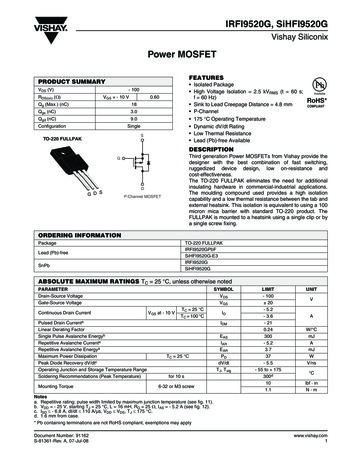
IRFI9520G, SiHFI9520GVishay SiliconixPower MOSFETFEATURESPRODUCT SUMMARYVDS (V) Isolated Package High Voltage Isolation 2.5 kVRMS (t 60 s;f 60 Hz) Sink to Lead Creepage Distance 4.8 mm P-Channel 175 C Operating Temperature Dynamic dV/dt Rating Low Thermal Resistance Lead (Pb)-free Available- 100RDS(on) (Ω)VGS - 10 V0.60Qg (Max.) (nC)18Qgs (nC)3.0Qgd (nC)9.0ConfigurationSingleSTO-220 FULLPAKAvailableRoHS*COMPLIANTDESCRIPTIONThird generation Power MOSFETs from Vishay provide thedesigner with the best combination of fast switching,ruggedized device design, low on-resistance andcost-effectiveness.The TO-220 FULLPAK eliminates the need for additionalinsulating hardware in commercial-industrial applications.The moulding compound used provides a high isolationcapability and a low thermal resistance between the tab andexternal heatsink. This isolation is equivalent to using a 100micron mica barrier with standard TO-220 product. TheFULLPAK is mounted to a heatsink using a single clip or bya single screw fixing.GG D SDP-Channel MOSFETORDERING INFORMATIONPackageTO-220 GLead (Pb)-freeSnPbABSOLUTE MAXIMUM RATINGS TC 25 C, unless otherwise notedPARAMETERDrain-Source VoltageGate-Source VoltageContinuous Drain CurrentPulsed Drain CurrentaLinear Derating FactorSingle Pulse Avalanche EnergybRepetitive Avalanche CurrentaRepetitive Avalanche EnergyaMaximum Power DissipationPeak Diode Recovery dV/dtcOperating Junction and Storage Temperature RangeSoldering Recommendations (Peak Temperature)Mounting TorqueSYMBOLVDSVGSVGS at - 10 VTC 25 CTC 100 CIDIDMTC 25 Cfor 10 s6-32 or M3 screwEASIAREARPDdV/dtTJ, TstgLIMIT- 100 20- 5.2- 3.6- 210.24300- 5.23.737- 5.5- 55 to 175300d101.1UNITVAW/ CmJAmJWV/ns Clbf · inN·mNotesa. Repetitive rating; pulse width limited by maximum junction temperature (see fig. 11).b. VDD - 25 V, starting TJ 25 C, L 16 mH, RG 25 Ω, IAS - 5.2 A (see fig. 12).c. ISD - 6.8 A, dI/dt 110 A/µs, VDD VDS, TJ 175 C.d. 1.6 mm from case.* Pb containing terminations are not RoHS compliant, exemptions may applyDocument Number: 91162S-81361-Rev. A, 07-Jul-08www.vishay.com1
IRFI9520G, SiHFI9520GVishay SiliconixTHERMAL RESISTANCE RATINGSPARAMETERSYMBOLTYP.MAX.Maximum Junction-to-AmbientRthJA-65Maximum Junction-to-Case (Drain)RthJC-4.1UNIT C/WSPECIFICATIONS TJ 25 C, unless otherwise notedPARAMETERSYMBOLTEST CONDITIONSMIN.TYP.MAX.UNITVDSVGS 0 V, ID 250 µA- 100--VΔVDS/TJReference to 25 C, ID - 1 mA-- 0.10-V/ CVGS(th)VDS VGS, ID 250 µA- 2.0-- 4.0VnAStaticDrain-Source Breakdown VoltageVDS Temperature CoefficientGate-Source Threshold VoltageGate-Source LeakageZero Gate Voltage Drain CurrentDrain-Source On-State ResistanceForward TransconductanceIGSSIDSSRDS(on)gfsVGS 20 V-- 100VDS - 100 V, VGS 0 V--- 100VDS - 80 V, VGS 0 V, TJ 150 C--- 9.6--29--21--25--4.5-ID - 3.1 AbVGS - 10 VVDS - 50 V, ID - 3.1AbµADynamicInput CapacitanceCissOutput CapacitanceCossReverse Transfer CapacitanceCrssDrain to Sink CapacitanceCTotal Gate ChargeQgGate-Source ChargeQgsGate-Drain ChargeQgdTurn-On Delay Timetd(on)Rise TimeTurn-Off Delay TimeFall TimeInternal Drain InductanceInternal Source Inductancetrtd(off)VGS 0 V,VDS - 25 V,f 1.0 MHz, see fig. 5f 1.0 MHzVGS - 10 VID - 6.8 A, VDS - 80 V,see fig. 6 and 13bVDD - 50 V, ID - 6.8 A,RG 18 Ω, RD 7.1 Ω,see fig. 10btfLDLSBetween lead,6 mm (0.25") frompackage and center ofdie contactDpFnCnsnHG-7.5---- 5.2--- 21--- 6.3V-100200ns-0.330.66µCSDrain-Source Body Diode CharacteristicsContinuous Source-Drain Diode CurrentISPulsed Diode Forward CurrentaISMBody Diode VoltageVSDBody Diode Reverse Recovery TimetrrBody Diode Reverse Recovery ChargeQrrForward Turn-On TimetonMOSFET symbolshowing theintegral reversep - n junction diodeDAGSTJ 25 C, IS - 5.2 A, VGS 0 VbTJ 25 C, IF - 6.8 A, dI/dt 100 A/µsbIntrinsic turn-on time is negligible (turn-on is dominated by LS and LD)Notesa. Repetitive rating; pulse width limited by maximum junction temperature (see fig. 11).b. Pulse width 300 µs; duty cycle 2 %.www.vishay.com2Document Number: 91162S-81361-Rev. A, 07-Jul-08
IRFI9520G, SiHFI9520GVishay SiliconixTYPICAL CHARACTERISTICS 25 C, unless otherwise notedFig. 1 - Typical Output Characteristics, TC 25 CFig. 3 - Typical Transfer CharacteristicsFig. 2 - Typical Output Characteristics, TC 175 CFig. 4 - Normalized On-Resistance vs. TemperatureDocument Number: 91162S-81361-Rev. A, 07-Jul-08www.vishay.com3
IRFI9520G, SiHFI9520GVishay SiliconixFig. 5 - Typical Capacitance vs. Drain-to-Source VoltageFig. 6 - Typical Gate Charge vs. Gate-to-Source Voltagewww.vishay.com4Fig. 7 - Typical Source-Drain Diode Forward VoltageFig. 8 - Maximum Safe Operating AreaDocument Number: 91162S-81361-Rev. A, 07-Jul-08
IRFI9520G, SiHFI9520GVishay SiliconixRDVDSVGSD.U.T.RG VDD- 10 VPulse width 1 µsDuty factor 0.1 %Fig. 10a - Switching Time Test Circuittd(on)trtd(off) tfVGS10 %90 %VDSFig. 9 - Maximum Drain Current vs. Case TemperatureFig. 10b - Switching Time WaveformsFig. 11 - Maximum Effective Transient Thermal Impedance, Junction-to-CaseIASLVary tp to obtainrequired IASVDSVDSD.U.TRGIAS0.01 ΩFig. 12a - Unclamped Inductive Test CircuitDocument Number: 91162S-81361-Rev. A, 07-Jul-08VDDtp- 10 Vtp V DDVDSFig. 12b - Unclamped Inductive Waveformswww.vishay.com5
IRFI9520G, SiHFI9520GVishay SiliconixFig. 12c - Maximum Avalanche Energy vs. Drain CurrentCurrent regulatorSame type as D.U.T.50 kΩQG- 10 V12 V0.2 µF0.3 µFQGS-QGDD.U.T.VG VDSVGS- 3 mAChargeIGIDCurrent sampling resistorsFig. 13a - Basic Gate Charge Waveformwww.vishay.com6Fig. 13b - Gate Charge Test CircuitDocument Number: 91162S-81361-Rev. A, 07-Jul-08
IRFI9520G, SiHFI9520GVishay SiliconixPeak Diode Recovery dV/dt Test CircuitD.U.T. Circuit layout considerations Low stray inductance Ground plane Low leakage inductancecurrent transformer --RG dV/dt controlled by RG ISD controlled by duty factor "D" D.U.T. - device under test - VDDCompliment N-Channel of D.U.T. for driverDriver gate driveP.W.PeriodD P.W.PeriodVGS - 10 V*D.U.T. ISD waveformReverserecoverycurrentBody diode forwardcurrentdI/dtD.U.T. VDS waveformDiode recoverydV/dtRe-appliedvoltageVDDBody diode forward dropInductor currentRipple 5 %*ISDVGS - 5 V for logic level and - 3 V drive devicesFig. 14 - For P-ChannelVishay Siliconix maintains worldwide manufacturing capability. Products may be manufactured at one of several qualified locations. Reliability data for SiliconTechnology and Package Reliability represent a composite of all qualified locations. For related documents such as package/tape drawings, part marking, andreliability data, see http://www.vishay.com/ppg?91162.Document Number: 91162S-81361-Rev. A, 07-Jul-08www.vishay.com7
Legal Disclaimer Noticewww.vishay.comVishayDisclaimer ALL PRODUCT, PRODUCT SPECIFICATIONS AND DATA ARE SUBJECT TO CHANGE WITHOUT NOTICE TO IMPROVERELIABILITY, FUNCTION OR DESIGN OR OTHERWISE.Vishay Intertechnology, Inc., its affiliates, agents, and employees, and all persons acting on its or their behalf (collectively,“Vishay”), disclaim any and all liability for any errors, inaccuracies or incompleteness contained in any datasheet or in any otherdisclosure relating to any product.Vishay makes no warranty, representation or guarantee regarding the suitability of the products for any particular purpose orthe continuing production of any product. To the maximum extent permitted by applicable law, Vishay disclaims (i) any and allliability arising out of the application or use of any product, (ii) any and all liability, including without limitation special,consequential or incidental damages, and (iii) any and all implied warranties, including warranties of fitness for particularpurpose, non-infringement and merchantability.Statements regarding the suitability of products for certain types of applications are based on Vishay’s knowledge oftypical requirements that are often placed on Vishay products in generic applications. Such statements are not bindingstatements about the suitability of products for a particular application. It is the customer’s responsibility to validate that aparticular product with the properties described in the product specification is suitable for use in a particular application.Parameters provided in datasheets and / or specifications may vary in different applications and performance may vary overtime. All operating parameters, including typical parameters, must be validated for each customer application by the customer’stechnical experts. Product specifications do not expand or otherwise modify Vishay’s terms and conditions of purchase,including but not limited to the warranty expressed therein.Except as expressly indicated in writing, Vishay products are not designed for use in medical, life-saving, or life-sustainingapplications or for any other application in which the failure of the Vishay product could result in personal injury or death.Customers using or selling Vishay products not expressly indicated for use in such applications do so at their own risk.Please contact authorized Vishay personnel to obtain written terms and conditions regarding products designed forsuch applications.No license, express or implied, by estoppel or otherwise, to any intellectual property rights is granted by this documentor by any conduct of Vishay. Product names and markings noted herein may be trademarks of their respective owners. 2017 VISHAY INTERTECHNOLOGY, INC. ALL RIGHTS RESERVEDRevision: 08-Feb-171Document Number: 91000
Document Number: 91162 www.vishay.com S-81361-Rev. A, 07-Jul-08 1 Power MOSFET IRFI9520G, SiHFI9520G Vishay Siliconix FEATURES Isolated Package