Transcription
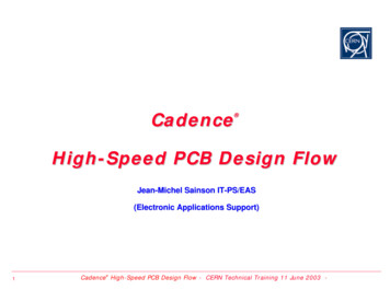
Cadence High-Speed PCB Design FlowJean-Michel Sainson IT-PS/EAS(Electronic Applications Support)1Cadence High-Speed PCB Design Flow - CERN Technical Training 11 June 2003 -
Training Description Objective Recommended for 2Cadence front-end PE14.2 high-speed printed circuit board design flowpresentation. Based on Constraint Manager concurrently with Concept-HDLschematic and SPECCTRAQuest/SigXplorer signal integrity analysis packageDigital electronics designers using Cadence CAD tools having signal integrity and/ortiming issues on their high-speed boardsDesigners working with Gigabit channels or using current fast standard logic families(LVCMOS, LVDS, LVPECL, HSTL, SSTL, GTL, etc.)Users of more traditional technologies on big board format such as VME9UCadence High-Speed PCB Design Flow - 11 June 2003 -
Programme 3High-Speed Board Design Issues & Solution Available @ CERNConstraint Manager PrinciplesBasic Layout Data Base SetupDesigners’ WorkflowsReal Case Study Description Demo: Before Layout Layout Implementation Demo: After LayoutConclusionAppendix 1: Constraint Manager Enabled FlowAppendix 2: IBIS Models Supply and CheckingAppendix 3: First Switch and Final Settle Delay Measurements PointsCadence High-Speed PCB Design Flow - 11 June 2003 -
High-Speed Board Design Issues&Solution Available @ CERN4Cadence High-Speed PCB Design Flow - CERN Technical Training 11 June 2003 -
High-Speed Board for LHCb Experiment NP4GS3 Network Processor Daughter Board14 layers 10%Controlled ImpedanceBoardDATA-ALIGNED SYNCHRONOUS LINKS (DASL)2 x 8 EIA/JEDEC JESD8-6 standardchannel for differential HSTL(Up to 625 Mbps per channel)1088-Pin(CCGA) PackageFine Pitch 1.27 mm815 I/ODRAM x16DDR(D3)(D2)(D1)(D0)1.8V125 MHZ2x512kx18SRAM512kx18SRAM(LU)(SCH)DRAM ControlNP4GS3DRAMControl53.3 Mx16DDRDATA(DS0)2x8Mx16DDRDATA(DS1)DMUsDRAM DataDRAM DataA B CDouble Data Rate SDRAM INTERFACEJEDS8-9A SSTL2 StandardStub Series Terminated Logic for 2.5VCLK 133 MHZ5D2 x 4 GIGABIT MEDIA INDEPENDENT INTEFACE UNITS (GMII)(4 GIGABIT ETHERNET)Full Duplex 8 bit data Bus 125 MHz ClockLVTTLCadence High-Speed PCB Design Flow - High-Speed Board Design Issues & Solutions @ CERN -
High-Speed Board Design Issues Typical High-Speed Board Design Issues 6Fast edge rates 500psVery high pin densityVia number controlSingle ended and differential Zo controlled impedanceVarious termination types (thevenin, serie,etc.)Min/max propagation delaysCross-talkTotal etch lengthRelative (Matched) length propagation delayPackage parasitic effectsClock & Buses timing constraints with accurate set up & hold Multiple constraints exist on each net Integrating Requirements is Essential for Success!Cadence High-Speed PCB Design Flow - High-Speed Board Design Issues & Solutions @ CERN -
Cadence’s PSD14.2High-Speed PCB Design Flow Based on the New “Constraint Manager” Programme Linking Signal Explorer Expert (SigXplorer) pre and post layout exploration toolConcept-HDL schematic capture toolSPECCTRAQuest SI Expert post-layout SI ananlysis toolALLEGRO-Expert and SPECCTRA layout implementation toolsHigh-Speed PCB Design FlowExplorationCaptureConcept-HDLLayout Constraint dence High-Speed PCB Design Flow - High-Speed Board Design Issues & Solutions @ CERN -
Designer’s signerLayout Constraint ManagerSigXplorer Topologies Analysis ToolsTopologies development, signal integrity analysisElectrical constraints developmentElectrical constraints capture with Constraint Manager Connected to Concept-HDL (CM2C)and/or SigXplorerLayout Database Setup under SPECCTRAQuest 8SigXplorerSchematic Capture under Concept-HDL SigXplorerExploration under SigXplorer SigXplorerLayout database setup with Constraint Manager Connected to SPECCTRAQuest (CM2SQ)Electrical constraints mappingCadence High-Speed PCB Design Flow - High-Speed Board Design Issues & Solutions @ CERN -
SigXplorer in the High-Speed Design FlowEX: Pre layout (Exploration) PhaseTOPOLOGY development underSigXplorer9Cadence High-Speed PCB Design Flow - High-Speed Board Design Issues & Solutions @ CERN -
Layout Designer’s pt-HDLLayout Constraint ManagerSigXplorer SigXplorerSigXplorerImplementation Phase 10SigXplorerElectrical constraints driven placement and routage with Constraint ManagerConnected to Allegro-Expert layout editor (CM2AE)Interactive (Allegro) or automatic (SPECCTRA) placement and routageCadence High-Speed PCB Design Flow - High-Speed Board Design Issues & Solutions @ CERN -
Constraint Manager Principles11Cadence High-Speed PCB Design Flow - CERN Technical Training 11 June 2003 -
What is Constraint Manager (CM)? Constraint Manager is a Spreadsheet based Application handling OBJECTSand Electrical Constraints Sets (ECSets)Objects12Cadence High-Speed PCB Design Flow - Constraint Manager Principles -
Constraint Manager Objects (1/5) Pin Pair A pin-pair represents a pair of logically connected pins, often a driver-receiverconnection.You may specify pin-pairs explicitly (for example, U1.8 – U2.8), or they can be derivedbased on the following criteria:z longest pin-pairz longest driver-receiver pairz all driver-receiver pairPin-PairR1.2 – U3.8Pin-PairU1.8 – U2.8Pin-PairU2.8 – R1.1Pin-PairU1.8 – U3.8 13Pin-pair Objects Not Supported in Concept-HDL 14.2Cadence High-Speed PCB Design Flow - Constraint Manager Principles -
Constraint Manager Objects (2/5) Net Basic connectivity as defined in the schematicXNet An eXtended Net XNet chains through passive discrete device (s)(resistor, inductor, capacitor)XNet can also traverse connector and cables in a multiboard configurationNet1Net2Net3XNet 14XNet Objects Not Supported in Concept-HDL 14.2Cadence High-Speed PCB Design Flow - Constraint Manager Principles -
Constraint Manager Objects (3/5) Diff Pair An electrical differential pair Diff-Pair represents a coupled pair of Net or XNet which willbe routed differentiallyDiff-Pair Diff Pair Objects Not Supported in Concept-HDL 14.2Bus A Bus represents a named collection of diff-pairs, Nets or XNetsBus15Cadence High-Speed PCB Design Flow - Constraint Manager Principles -
Constraint Manager Objects (4/5) Relative/Matched Group A Relative/Matched Group represents a user-specified collection of pin-pairs constrainedby a relative or match delay or lengthThe following attributes are used to characterize a Relative/Match Groupz Target : The pin-pair that is referenced by all pin-pairs in the groupz Delta: The difference between each pin-pair member and the target pin-pair.z Tolerance: The tolerance allowed when matching members in the groupExample (Top Layer View)Matched Group (M1)M1 Data 0.7 DQS0To maintain a matched propagation delay, 8Data Nets (4 in the top layer), are extendedto match the length of (DQS0) strobeTarget (Strobe DQS0)16Cadence High-Speed PCB Design Flow - Constraint Manager Principles -
Constraint Manager Objects (5/5) Design A Design represents a stand-alone board or a board in a systemIn a multi-board configuration, each board becomes a separate design in the systemSystem A System represents a configuration of designs (boards) including XNets that traversethese design and their interconnecting cables and connectorsSystem17DesignsCadence High-Speed PCB Design Flow - Constraint Manager Principles -
Object HierarchyInheritance Goal is to assign constraints at the highest possible level 18Constraints that you specify at the top level of the hierarchy become inherited by the nextlower-level objectSpecial exception cases can be handled by overrides at lower levelCadence High-Speed PCB Design Flow - Constraint Manager Principles -
Electrical Constraint Sets (ECSets) What is an ECSet? AN ECSet is a collection of generic simulated and/or computed CONSTRAINTSrequirements.You define one or more ECSets to capture design requirementsYou then assign the appropriate ECSet to objects in your designECSets TypesSimulated (post layout)Computed (real time)19Cadence High-Speed PCB Design Flow - Constraint Manager Principles -
Computed ECSets TypesRouting ECSets Routing constraints analysis (handling lengths/prop delay and impedances) does notneed simulation,Are calculated and flagged in real time by Constraint Manager (CM)Routing Constraint Violation ExampleElectrical DRC (ED)displayed underSPECCTRAQuest20Same “Prop Delay/Length”constraint violationdisplayed under CM2SQCadence High-Speed PCB Design Flow - Constraint Manager Principles -
Simulated ECSets TypesSignal Integrity & TimingConstraints 21Signal Integrity & Timingconstraints analysis values are theresult of analogue simulationsElectrical Constraints simulationsresults are displayed in CMworksheets and/orSPECCTRAQuest simulationreportsThe Cadence TLSim simulator is aSPICE-like engine using DMLCadence proprietary formatDML (Device Model) format is theCadence implementation of IBISbehavioural signal integrity modelsfor signal integrity analysisIBIS is a “component centric”standard ideal for board levelsimulation.It is widely supported by ICsmanufacturersSimulations results displayedin CM Switch/Settle Delays worksheetCadence High-Speed PCB Design Flow - Constraint Manager Principles -
Invoking Constraint Manager Standalone forDesign Exploration From Concept-HDL (CM2C) Tools Æ Constraints Æ EditShould only be run on a PACKAGED schematicConstraint Manager invoked from Concept-HDL does not presently support PinPairs, XNets and Differential pair (only supported by layout data base)From SPECCTRAQuest (CM2SQ) 22Unix prompt type Æ consmgrSetup Æ Electrical Constraint Spreadsheet IconCadence High-Speed PCB Design Flow - Constraint Manager Principles -
Constraint Manager User Interface (1/7) Worksheet Selector The worksheet selector is the only way to select (open) the various worksheetswithin 23The “Electrical Constraint Set”worksheets are used for creatingand/or editing the Rule SetsSelectedWorksheetsThe “Net” worksheets are used forinterfacing with the design objectssuch as applying the rules or seeingif they can be metCadence High-Speed PCB Design Flow - Constraint Manager Principles -
Constraint Manager User Interface (2/7) Example: Min/Max Propagation Delay Worksheet uesCadence High-Speed PCB Design Flow - Constraint Manager Principles -
Constraint Manager User Interface (3/7) Objects Column in a Nets Folder Routing WorksheetDesignNetPin PairBusesXNetPin Pairs25Cadence High-Speed PCB Design Flow - Constraint Manager Principles -
Constraint Manager User Interface (4/7) ECSet Mapping to Objects On individual Net, selected Nets, Bus, selected Buses, etc.3250 Mils Longest/Shortest Driver/Receiver Max lengthCNTRL ADDECSet“CNTRL ADD”EcsetMapped toD6 ADDR 0.3 26Cadence High-Speed PCB Design Flow - Constraint Manager Principles -
Constraint Manager User Interface (5/7) Viewing ECSets ReferencesCNTRL ADD ECSetapplied to BUSESDA DQS ECSetapplied to BUSESCNTRL ADD ECSetapplied to NETS27Cadence High-Speed PCB Design Flow - Constraint Manager Principles -
Constraint Manager User Interface (6/7) Colour Coding Cells are BLACK and BLUE colour coded to indicate inheritance for constraints.Results status displayed in YELLOW, GREEN or REDBlue indicating theECSet has beenoriginally appliedin this cellBlue indicating that this cellwas overwritten (3500 Mils)on NET D6 ADDR0Black indicating theECSet are inherited oneach NET283250 Mils in black indicatingthat this value is inherited onPin Pair from “CNTRL ADD”ECSet (Prop Delay/MaxLength) constraint valueCadence High-Speed PCB Design Flow - Constraint Manager Principles -
Constraint Manager User Interface (7/7) STATUS BAR Information Type Progress meter for simulationsBrief description of commandsReasons why items are greyed outPlacing cursor over an object inthe display provides informationon the STATUS BAR below29Cadence High-Speed PCB Design Flow - Constraint Manager Principles -
Constraint Manager Enabled FlowVsTraditional Flow First Time you Invoke Constraints Manager from Concept-HDLand/or SPECCTRAQuest-Expert If you Have Launch Constraint Manager by Mistake 30You are in CONSTRAINT MANAGER ENABLED FLOWYou can not go back automatically to the traditional flowYou can go back to the TRADITIONAL DESIGN FLOW deleting files and directorautomatically created, SEE APPENDIX1: Constraint Manager Enabled FlowCadence High-Speed PCB Design Flow - Constraint Manager Principles -
Basic Layout Data BaseSetup31Cadence High-Speed PCB Design Flow - CERN Technical Training 11 June 2003 -
Basic Layout Data Base SetupFrom SPECCTRAQuest-ExpertLayout Cross Section Define by Designer WITHAGREEMENT OF LAYOUTDESIGNER EXPERT AND/ORBOARD MANUFACTURERYou can define a set of typicalmicrostrip and stripline. Later inthe design flow it will be easy toadd or erase conductors layersSQ Setup Form:Setup ÆCross SectionProvides data for SPECCTRAQuestField Solver to compute accuratetransmission line modelling of tracesDetermines trace characteristicssuch as impedance and propagationvelocityMicrostrip or Stripline Impedances arecomputed in real time by the Field Solver eachtime we change a parameter (line width etc.),helping designer to find optimum combination ofmaterial, thickness and PCB CLASS32Cadence High-Speed PCB Design Flow - Basic Layout Data Base Setup -
Basic Layout Data Base SetupFrom SPECCTRAQuest-Expert Identifying DC Nets 33SQ Identify DC Nets Form:Logic Æ Identify DC Nets.Makes sure simulations inSPECCTRAQuest or SigXphave the correct voltage forcircuitsPrevents XNets from includingwrong netsCadence High-Speed PCB Design Flow - Basic Layout Data Base Setup -
Basic Layout Data Base SetupFrom SPECCTRAQuest-ExpertDiscrete (R, L, C) DML SignalModel Assignment 34Signal Model Assignment Form:Analyse Æ SI/EMI Sim ÆModel.DML discrete modelsassignment are the minimummodels assignment (also calledEspice models) that must bedone for all analysis cases(Routing or SI & Timing)Without this assignment thesystem will not be able todevelop XNet from the layoutdatabaseIf component libraries includeCLASS, VALUE and PINUSE,Auto Setup buttonautomatically setup this processfor 2 pin discreteDiscrete with more than 2 pinscould be easily created viaCreate Model buttonEx: DML (or ESPice)models assigned toresistors terminationsThis button willautomatically makeEspice models for all 2pins discretesCadence High-Speed PCB Design Flow - Basic Layout Data Base Setup -
Basic Layout Data Base SetupFrom SPECCTRAQuest-ExpertOptional IBIS (DML) ModelsAssignment 35Signal Model Assignment Form:Analyse Æ SI/EMI Sim Æ Model.Optional assignment that must bedone on ICsSimulated analysis supported bySignal Integrity or Timingworkbooks needs IBIS modelsassignmentSee APPENDIX 2: IBIS ModelsSupply and CheckingIt is not necessary to assign IBISmodels for computed analysis(see later workflow n)Default models are automaticallyassigned by the system.Ex: IBIS (DML) models:6 x K4H280838C TCDDR SDRAM memorymodelEx: IBIS (DML) models:1x NP4GS3B NetworkProcessor ModelStart IBIS (DML)process assignment foractive devices (ICs)Cadence High-Speed PCB Design Flow - Basic Layout Data Base Setup -
Designers’ Workflows36Cadence High-Speed PCB Design Flow - CERN Technical Training 11 June 2003 -
Typical Designers’ WorkflowsDesigners’ Workflows TypeTo implement layout rulesfrom componentsmanufacturerXRules basedYRules basedwith PCB simulationsTo implement layout rulesfrom componentsmanufacturerThen check them (simulate)on post-layout boardZConstraints developmentTo develop yourself layoutrules. Any guideline availablefrom manufacturerThen implement them[Constraints developmentwith PCB simulations37PurposeTo develop yourself layoutrules. Any guideline availablefrom manufacturerThen implement and checkthem (simulate) on postlayout boardPost-layoutSignal Integrityand/or TimingsimulationsneededNeed of IBISmodelsNoNoYesYesNoYesYesYesCadence High-Speed PCB Design Flow - Designers’ Workflow -
- Workflow X - Rules BasedDCCaptureAImplementationLayout DTB SetupConcept-HDLConstrainedSchematicDesign SyncSPECCTRAQuestExport PhysConstrainedBoardDatabaseImport Phys.To/FromLayout(.BRD)Before layoutConstraint ManagerConnected toConcept-HDLHConstraint ManagerConnected toSPECCTRAQuestEBECSetsSigXplorer (.TOP)Exploration 38FECSets ConstrainedTopologiesPhysicalNETsAfter layoutA Æ schematic capture with Concept-HDLB Æ ECSets capture under Constraint Manager (CM2C)C Æ export physical (Packager-XL NETREV)D Æ Basic layout DTB setup: cross section, DC netsidentification, discrete (R, L, C) Autosetup modelsassignmentE Æ ECSets mapping to physical NETsF Æ post layout constraints check (calculated)H Æ (optional) ECSets change back annotationCadence High-Speed PCB Design Flow - Designers’ Workflow -
- Workflow Y - Rules Based With PCB SimulationsImplementationD1DCCaptureALayout DTB SetupConcept-HDLConstrainedSchematicDesign SyncSPECCTRAQuestExport PhysConstrainedBoardDatabaseImport Phys.To/FromLayout(.BRD)Before layoutConstraint ManagerConnectedto Concept-HDLHConstraint ManagerConnectedto r ConstrainedTopologies(.TOP) A B C D E F H Æ same as Workflow XD1 Æ Ibis libraries setup & models assignmentG Æ simulated constraints analysis ( from Signal Integrity &Timing Workbooks)Exploration39After layoutCadence High-Speed PCB Design Flow - Designers’ Workflow -
- Workflow Z - Constraints DevelopmentImplementationDCCaptureALayout DTB SetupDesign SyncConcept-HDLSPECCTRAQuestTo/FromLayoutExport port Phys.(.BRD)Before layoutConstraint ManagerConnectedto Concept-HDLHConstraint ManagerConnectedto SPECCTRAQuestEECSetsPhysicalNETsAfter layoutFECSetsB3 SigXplorerB2ConstrainedTopologies (.TOP)B1Exploration40 A C D E F H Æ same as Workflow XB1 Æ Ibis (Dml) libraries declarationB2 Æ constrained topologies developmentfrom SigXplorerB3 Æ constrained topologies importationin Constraint Manager connected to ConceptCadence High-Speed PCB Design Flow - Designers’ Workflow -
- Workflow [ - Constraints DevelopmentWith PCB SimulationsD1DCCaptureALayout DTB SetupDesign SyncConcept-HDLSPECCTRAQuestTo/FromLayoutExport port Phys.(.BRD)Before layoutConstraint ManagerConnectedto Concept-HDLHConstraint ManagerConnectedto SPECCTRAQuestEECSetsPhysicalNETsAfter layoutFECSetsGB3SigXplorerB2ConstrainedTopologies (.TOP)B1A B1 B2 B3 C D E F H Æ same as Workflow ZD1 Æ Ibis models assignmentG Æ simulated constraints analysis ( from Signal Integrity &Timing Workbooks)Exploration41Cadence High-Speed PCB Design Flow - Designers’ Workflow -
Real Case Study(Description)42Cadence High-Speed PCB Design Flow - CERN Technical Training 11 June 2003 -
Demo Scope To layout WITH MANUFACTURER GUIDELINES a subset of NP4GS3 DDRSDRAM interfaceDRAM x16DDR(D3)(D2)(D1)(D0)1.8V125 MHZ2x512kx18SRAM512kx18SRAM(LU)(SCH)DRAM ControlNP4GS3DRAMControl53.3 Mx16DDRDATA(DS0)2x8Mx16DDRDATA(DS1)DMUsDRAM DataDRAM DataA B C64 MB DDR SDRAM6 Samsung (32X4) K4H280438C-TCA2I/O technologies Stub series Terminated Logic 2.5V (SSTL2) &CMOS66 pins TSOP II Package43DD6 INTERFACE ARCHITECTURE18 bits DATA BUS13 bits ADDRESS BUSDifferential ClockClock Cycle 133 MHZDouble-data rate architecture; two transfers per clock cycleI/O technologies Stub series Terminated Logic 2.5V (SSTL2)&CMOSCadence High-Speed PCB Design Flow - Real Case Study (Description)-
CNTRL & ADDR Manufacturer Guidelines CNTRL ADDR Lines Constraints Control and address lines are six-drop lines terminated into a 50 Ω equivalent circuitBoard Stackup controlled impedance 55 Ω 10 %The distance from NP4GS3 to the furthest SDRAM must not exceed 3.25 inchesThe stub to the SDRAM pin should not be more than 0.25 inchesDDR SDRAMDDR SDRAM (32M x 4)DDR SDRAM (32M x 4)DDR SDRAM (32M x 4)SAMSUNGDDR SDRAM (32M x 4)SAMSUNGK4H280438CDDR SDRAM (32M x 4)SAMSUNGK4H280438C(32M x 4)SAMSUNG K4H280438C50 Ω SUNGK4H280438CK4H280438CStub 0.25 inches2.5V2.5V100 Ohms2.5V100 Ohms2.5V100 Ohms13 ADDRESS LINES100 OhmsNP4GS3100 Ohms10 CONTROL LINES100 Ohms100 Ohms100 OhmsZo 55 Ω 10%L 3.25 inches44Cadence High-Speed PCB Design Flow - Real Case Study (Description)-
DATA & DQS Manufacturer Guidelines DA DQS Lines Constraints All DATA and DQS nets must be terminated with a 22-29 Ω series resistor placed nomore than one inch from the NP4GS3No more than 25 % of the trace should be on the NP4GS3 side of the terminating resistorEach set of DATA and DQS lines must be no shorter than one inch and no longer than3.25 inchesFor each set of four DATA lines and its respective DQS line, there can be no morethan 70 ps of flight time difference from the NP4GS3 to the RAM. Use IBIS simulation tobe sure that there no more than 70 ps difference between DQS and its correspondingDATA linesDDRDDRSDRAMDDRSDRAMSDRAM (32M x 4) (32M x 4)(32M x DRAMDDRSDRAMSDRAM (32M x 4) (32M x 4)(32M x 4)SAMSUNGSAMSUNGK4H280438CSAMSUNGK4H280438C1 inch L 3.25 inchesK4H280438C 1 inchK4H280438C4 DATA LINES22-29OhmsDQS (Vs) 4 DATALines flight timeSkew 70 ps4 DATA LINESDQS122-29Ohms4 DATA LINES1 DATA LINES4522-29Ohms4 DATA4 DATALINESLINESZo 55 Ω 10% 1 DATA DQS4DQS5Cadence High-Speed PCB Design Flow - Real Case Study (Description)-
Demo WorkflowD1DCCaptureALayout DTB SetupDesign SyncConcept-HDLSPECCTRAQuestTo/FromLayoutExport port Phys.(.BRD)Before layoutConstraint ManagerConnectedto Concept-HDLConstraint ManagerConnectedto SPECCTRAQuestPhysicalNETsEECSetsAfter layoutFECSetsBGB3 SigXplorerB2ConstrainedTopologies (.TOP)B1Exploration 46A Æ Concept-HDL: schematic captureB Æ CM2C: CNTRL ADD ECSets captureB1Æ SigXp: Ibis (Dml) libraries declaration(DDR SDRAM & NP4GS3) before DA DQS(XNet) topology captureB2Æ SigXp: DA DQS constrainedtopology captureB3Æ Concept-HDL : DA DQS constrained topologyimportation from SigXp (ECSet) C Æ Concept-HDL: export physical(Packager-XL NETREV)D Æ SPECCTRAQuest-Expert: Basic layoutDTB setup; cross section, DC netsIdentification, discrete (R, L, C)Autosetup models assignmentD1Æ SPECCTRAQuest-Expert: Ibis modelsassignment:(6 x DDR SDRAM & 1 x NP4GS3)E Æ CM2SQ:CNTRL ADD & DA DQS: ECSetsmapping to physical NETsF Æ CM2SQ:post layout constraints checkG Æ CM2SQ:DATA Timing skew simulationCadence High-Speed PCB Design Flow - Real Case Study (Description)-
Real Case Study(Demo: Before Layout)47Cadence High-Speed PCB Design Flow - CERN Technical Training 11 June 2003 -
Concept-HDL: Schematic Capture [ Step A ]48Cadence High-Speed PCB Design Flow - Real Case Study (Demo: Before Layout) -
CM2C: CNTRL ADD ECSet Capture [ Step B ] To Create an object From CM2C: Objects ÆCreate ÆElectrical CSet.Stub length for daisy chainroutingDaisy-Chain scheduleconsists of connecting the pinsof the topology with minimumconnection length but onlyallowing each pin to connect toa maximum of two other pins.Mapping mode is used whenthe ECSet schedule is appliedto XNets/Nets in physical database.Pinuse map the ECSet’s pinsto the Net using the PINUSEsetting.49Cadence High-Speed PCB Design Flow - Real Case Study (Demo: Before Layout) -
Comments on CM2C Wiring WorksheetMapping Mode & Pre-Defined SchedulesPre-defined Mapping Mode: Pinuse Refdes Pinuse and Refdes Clear (any) 50Pre-defined Shedule: Minimum spanning Tree Daisy-chain Source-Load Daisy-chain Star Far-end cluster Clear (any)XNets scheduling is notpre-defined by the system. Butany structure of TOPOLOGYTEMPLATE could be capturedthen imported from SigXplorerFollowing steps [ B1 B2 B3 ] are Mandatory to Capture DA DQS XNet Topology TemplateCadence High-Speed PCB Design Flow - Real Case Study (Demo: Before Layout) -
SigXp: Ibis Libraries Declaration forDA DQS Topology Capture [ Step B1 ] Libraries Declaration From SigXp: Analyse ÆLibrariesnp4gs3b.ibis (or dml)library file delivered bythe manufacturer28h4088a.ibis(or dml) library filedownloaded fromSAMSUNG Web SiteModels used for DA DQSconstrainedtopology development(next slide)51Cadence High-Speed PCB Design Flow - Real Case Study (Demo: Before Layout) -
SigXp: DA DQSConstrained Topology Capture (1/4) [ Step B2 ] DA DQS Topology Edition File: da dqs.topNP4GS3 Packaged IBIS I/O ModelSSTL2 TechnologyDDR SDRAM Packaged IBIS I/O ModelSSTL2 TechnologyConstrained Topology(da dqs.top file)55 Ohms Transmission Lines52Cadence High-Speed PCB Design Flow - Real Case Study (Demo: Before Layout) -
SigXp: DA DQSConstrained Topology Capture (2/4) [ Step B2 ] To capture Constraints 53From SigXp: Set ÆConstraintsDA DQS Impedance Constraints Capture DA DQS Length Constraints CaptureCadence High-Speed PCB Design Flow - Real Case Study (Demo: Before Layout) -
SigXp: DA DQSConstrained Topology Capture (3/4) [ Step B2 ] DA DQS M1 Skew Rule CaptureA Relative propagation delayconstraint identifies a group of pinspairs with DELTA and tolerance.One of the pin pair will be later in thephysical data base selected as theTARGET and all of other pin pairs willbe matched against this target withinthe given delta and tolerance.Rule Name “DA DQS M1”M1 Matched group1 OBJECTAll members of the group; a set of 4DATA lines and its respective DQSline, must match ( 0 ns) within 15pstolerance.54Cadence High-Speed PCB Design Flow - Real Case Study (Demo: Before Layout) -
SigXp: DA DQSConstrained Topology Capture (4/4) [ Step B2 ] DA DQS Pin Sequencing Constraints CaptureMapping mode is used when the ECSetschedule is applied to XNets/Nets in thephysical data base.“Pinuse and Refdes” maps the ECSet’spins to the Net using the “da dqs”topology (pinuse & refdes) combination.Template schedule means the topologytemplate scheduling should follow“da dqs.top” topology55Cadence High-Speed PCB Design Flow - Real Case Study (Demo: Before Layout) -
Concept-HDL: DA DQS ECSetsImportation from CM2C [ Step B3 ] ECSets Importation in CM2C then Concept-HDL update CM2C: File ÆImport ÆElectrical CSet.Then Concept-HDL: Tools Æ Constraints ÆUpdate SchematicECSet: WiringWorksheetECSet: ImpedanceWorksheetECSet: Min/MaxPropagation DelaysWorksheetECSet: RelativePropagation DelayWorksheet56Cadence High-Speed PCB Design Flow - Real Case Study (Demo: Before Layout) -
Concept-HDL: Export Physical [ Step C ] Packaging with ECSets Exportation Concept-HDL: File ÆExport Physical.6 layers 55 Ω 10 % mezzanineboard templateElectrical constraints enabled57Cadence High-Speed PCB Design Flow - Real Case Study (Demo: Before Layout) -
SPECCTRAQuest-Expert: DTB SetupSteps [ D D1 ] Step D: Basic Layout DTB Setup Mezzanine Cross sectionz Mezzanine cross sectionz Already presented in previous “Basic Layout Data Base Setup” sectionMezzanine DC Netsz Three voltage (0V, 1,8V, 2.5V) DC Nets identificationz Already presented in previous “Basic Layout Data Base Setup” sectionTerminations (R) Models Assignmentz Auto Setup terminations models assignment (22 Ω, 100 Ω, 10 K Ω)z Already presented in previous “Basic Layout Data Base Setup” sectionStep D1: Ibis Models Assignmentzz58NP4GS3 & K4H280838C Ibis models assignmentAlready presented in previous “Basic Layout Data Base Setup” sectionCadence High-Speed PCB Design Flow - Real Case Study (Demo: Before Layout) -
CM2SQ: CNTRL ADD & DA DQS (1/4)ECSets Mapping [ Step E ] Impedance ECSet MappingECSetsECSetreferenceImpedance ECSet MappingonPhysical NETsObjectscolumn59Cadence High-Speed PCB Design Flow - Real Case Study (Demo: Before Layout) -
CM2SQ: CNTRL ADD & DA DQS (2/4)ECSets Mapping [ Step E ] Min/Max Length ECSet MappingCNTRL ADDR ECSetDATA0Pin PairMin/Max Length ECSetMappingon Physical NETsDA DQS ECSet60Cadence High-Speed PCB Design Flow - Real Case Study (Demo: Before Layout) -
CM2SQ: CNTRL ADD & DA DQS (3/4)ECSets Mapping [ Step E ] Wiring ECSet MappingCNTRL ADDR ECSetWiring ECSet MappingonPhysical NETsDA DQS ECSet61Cadence High-Speed PCB Design Flow - Real Case Study (Demo: Before Layout) -
CM2SQ: CNTRL ADD & DA DQS (4/4)ECSets Mapping [ Step E ] Relative Propagation Delay ECSet MappingMatch Group Object (M1)Automatically Createdon DA DQS ECSetMappingPassNo analyses result forthe targetMatch Group M15 Pin Pairs MembershipPin Pair Target(DQS0)62DQSO TARGETPin Pair SelectionCadence High-Speed PCB Design Flow - Real Case Study (Demo: Before Layout) -
Real Case Study(Layout Implementation)63Cadence High-Speed PCB Design Flow - CERN Technical Training 11 June 2003 -
Layout Designer’s WorkflownÆ [SPECCTRAQuestExpertorALLEGRO-ExpertHigh Speed ardDatabaseIt is recommended to review steps 1 to 5with the layout expert(.BRD)Constraint ManagerConnected toALLEGRO ( CM2A )\PhysicalNETs]ECSetsnÆ DTB check: layout impedance cross section with SPECCTRAQuest exclusivelyoÆ DTB check: DC Nets assignment with ALLEGRO-Expert or SPECCTRAQuestpÆ DTB check: discrete (R, L, C,) model assignment with ALLEGRO-Expert or SPECCTRAQuest[Æ DTB
7 Cadence's PSD14.2 High-Speed PCB Design Flow Based on the New "Constraint Manager" Programme Linking Signal Explorer Expert (SigXplorer) pre and post layout exploration tool Concept-HDL schematic capture tool SPECCTRAQuest SI Expert post-layout SI ananlysis tool ALLEGRO-Expert and SPECCTRA layout implementation tools SigXplorer Concept-HDL SPECCTRAQuest Allegro