Transcription
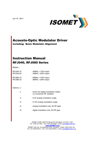
ISOMETJan 19, Rev1Acousto-Optic Modulator DriverIncluding: Basic Modulator AlignmentInstruction ManualRFJ040, RFJ080 SeriesModels RFJ040-15RFJ040-25: 40MHz, 12W output: 40MHz, 20W outputRFJ080-15RFJ080-25: 80MHz, 12W output: 80MHz, 20W outputOptions -x:-L: active low digital modulation (Gate)no connection RF disabled-V: 0-5V analog modulation range-X: 0-10V analog modulation range-A: analog modulation only. No RF gate-D: digital modulation only. No RF gateISOMET CORP, 5263 Port Royal Rd, Springfield, VA 22151, USA.Tel: (703) 321 8301, Fax: (703) 321 8546, e-mail: isomet@isomet.comwww.ISOMET.comISOMET (UK) Ltd, 18 Llantarnam Park, Cwmbran, Torfaen, NP44 3AX, UK.Tel: 44 1633-872721, Fax: 44 1633 874678, e-mail: isomet@isomet.co.uk
ISOMET1.GENERALThe RFJ0x0 combined Driver and Power Amplifiers are fixed frequency RF power sources specificallydesigned to operate with Isomet acousto-optic devices such as the M1133-aQ and M1377aQ series.The driver accepts independent digital and analogue modulating signals and provides a doublesideband amplitude modulated RF output to the acousto-optic modulator. A summary of the driverspecification is shown in the following table:ModelAmodCenter FrequencyOutput PowerRFJ040-151V40MHz 12.0 WattRFJ040-25-X10V40MHz 20.0 WattRFJ080-15-V5V80MHz 12.0 WattRFJ080-251V80MHz 20.0 WattFigure 2 is a functional block diagram of the driver. The center frequency of the driver is determinedby the free-running quartz-crystal oscillator at 40MHz or 80MHz. This frequency is accurate to within 25ppm and its stability is better than 25ppm; the oscillator is not temperature stabilized.The RFJ series feature two amplitude modulation controls; Amod and DmodAmodA high-frequency, diode ring modulator is used to apply proportional control (a.k.a. analogmodulation). Depending on the model, an input voltage swing of 1V (5V or 10V)* peak will result in100% depth of amplitude modulation.DmodA further solid state switch provides the Digital Modulation or RF Gating function.The input is 5V logic compatibleLogic High ONLogic Low OFFThe ON level is defined by the applied Amod input level* and the preset multi-turn PWR ADJpotentiometer. The PWR ADJ pot provides gain control and sets the maximum RF output power2
ISOMETAmod: proportional analog input.The input level must not exceed 2x the model specificAmod rating * (See Driver test data sheet).Dmod: digital logic inputLevel must not exceed 5.5 voltsThe rise and fall times for the amplifier from either modulation input is identical (approx’ 150nsec rise,50nsec fall) at full power.This amplifier is designed to operate at full rated power into a 50Ω load with 100% duty cycle.The output power level is set by a multi-turn potentiometer (PWR ADJ)NOTE : Maximum power fully clockwiseMounting the driver to heat conduicting surface is mandatory.The heatsink temperature must not exceed 50 C.An internal sensor will disable the driver when the temperature exceeds 50degCSERIOUS DAMAGE TO THE AMPLIFIER MAY RESULT IF THE TEMPERATURE EXCEEDS 70 C.SERIOUS DAMAGE TO THE AMPLIFIER MAY ALSO RESULT IF THE RF OUTPUT CONNECTORIS OPERATED OPEN-CIRCUITED OR SHORT-CIRCUITED.A low impedance DC power supply is required. The operating voltage is 24V or 28Vdc at a currentdrain of approximately 3A. The external power source should be regulated to 2% and the powersupply ripple voltage should be less than 200mV for best results.Higher RF output power is achieved at 28Vdc.Figures 3 and 5 show the main AO modulator parameters* Amod input voltage is model dependent 0-1V standard, Options -V 0-5V, -X 0-10V3
ISOMET2LED INDICATORSThe front panel LEDs serve to indicate a number of possible operating states.The LEDs [C] and [D] illuminate when the DC power is applied and the Interlocks are valid.Power AdjustABC [A] shows RED when the (thermal) Interlocks are enabled [B] shows YELLOW when the RF power amplifiers are Gated On (Dmod Logic High) [C] shows GREEN when DC power is appliedLEDs OffThe LED [A] will not illuminate if :a) the internal driver thermal interlock switch is open (Over temperature fault)b) the AOM thermal interlock switch is open (Over temperature fault)c) the AOM thermal interlock is not connected to the driver interlock inputd) the DC supply is off.The LED [B] may not illuminate or run dim if :a) the D Mod input is operating at low duty cycleb) the D Mod is not active (logic low)c) the DC supply is off.The thermal interlocks will reset once the AO device and / or RF driver are cooled below the switchingtemperature.- The driver thermal switch over temperature trip point is 50deg C- The typical AOM thermal switch over temperature trip point is 50deg CThe hysteresis of the thermal switch is 7-10deg C.Once in a fault state the coolant temperature may need to be reduced to reset the thermal switches.4
ISOMET3.INSTALLATION AND ADJUSTMENTRefer figure 4, 5 and Appendix A3.1Mount the driver and AO device to suitable heat conducting surfaces.Due to the high RF power dissipated in the AO modulator, it is paramount that the devicesare mounted to a heatsink.3.2With no d-c power applied, connect the 24V (or 28V) DC to the screw terminal.DO NOT APPLY POWER.3.3Connect the RF output BNC jack to the acousto-optic modulator (or a 50Ω RF load, if it isdesired to measure the modulator RF output power).3.4Connect the Interlock of the acousto-optic modulator (SMA, SMC, 3pin snap-in connector or 2pin molex) to the 3-pin snap INT connector on the RF driver (Binder connector, pins1 and 2).The interlock connection becomes open circuit disabling the RF output, if the temperature ofthe modulator exceeds 50ºC or the internal driver temperature exceeds 50ºC.3.5Adjustment of the RF output power is best done with amplifier connected to the acousto-opticmodulator. The Amplifier maximum output power is factory preset to approx’ 10W.The optimum RF power level required for the modulator to produce maximum firstorder intensity will be different at various laser wavelengths. Applying RF power inexcess of this optimum level will cause a decrease in first order intensity (a falseindication of insufficient RF power ) and makes accurate Bragg alignment difficult. Itis therefore recommended that initial alignment be performed at a low RF power level.Please refer to the AOM and RF driver test data sheets for RF power settings3.6Locate the PWR ADJ access on the driver end plate.3.7With an insulated alignment tool or screwdriver rotate the PWR ADJ potentiometer fully anticlockwise (at least 10 turns CCW) , then clockwise (CW) approx 4 turns.5
ISOMET3.8Apply DC to the amplifier.3.9Apply a 1.0V (5V or 10V)* constant modulation signal to the SMA input A Mod.3.9.1Apply a constant logic high level to the to the SMA input D Mod.Input the laser beam toward the centre of either aperture of the AOM/AOQ. Ensure the laserpolarization is correct for the AOM model and the beam height does not exceed the active apertureheight of the AOM.Start with the laser beam normal to the input optical face of the AOM and very slowly rotate the AOM(either direction). See Figure 4 below for one possible configuration.3.10Observe the diffracted first-order output from the acousto-optic modulator and the undeflectedzeroth order beam. Adjust the Bragg angle (rotate the modulator) to maximise first orderbeam intensity.3.11After Bragg angle has been optimized, slowly increase the RF power (rotate PWR ADJ CW)until maximum first order intensity is obtained.3.12The driver is now ready for use for modulation using both the digital and the analog inputs.* Amod input voltage is model dependent 0-1V standard, Options -V 0-5V, -X 0-10V6
ISOMET4.MAINTENANCE4.1CleaningIt is of utmost importance that the optical apertures of the AO device be kept clean and free ofcontamination. When the device is not in use, the cover apertures may be protected by kapton tape.It will probably be necessary in time to wipe the coated window surfaces of atmospherically depositedfilms. Although the coatings are hard and durable, care must be taken to avoid gouging of the surfaceand leaving residues. It is suggested that the coatings be wiped with a soft ball of brushed (shortfibres removed) cotton, slightly moistened with clean alcohol. Before the alcohol has had time to dryon the surface, wipe again with dry cotton in a smooth, continuous stroke. Examine the surface forresidue and, if necessary, repeat the cleaning.4.2TroubleshootingNo troubleshooting procedures are proposed other than a check of alignment and operatingprocedure. If difficulties arise, take note of the symptoms and contact the manufacturer.4.3RepairsIn the event of malfunction, discontinue operation and immediately contact the manufacturer orrepresentative. Due to the high sensitivity of RF tuning procedures and the possible damage whichmay result, no user repairs are allowed. Evidence that an attempt has been made to open the opticalhead will void the manufacturer's warranty.7
ISOMETRFJ 0x0 Standard VersionConnection SummarySignalTypeConnectorDigital Modulation / GATETTL high ( 2.5V) ONTTL low ( 0.8V)or no connection OffInputD Mod , SMAAnalogue Modulation*0.0V(off) to 1.0V(on)InputA Mod , SMAInterlockInputINT, Binder 719-3Signal pin 1Return pin 2(connect to AOmodulator ‘INT’)1Interlock Connector: 3-pin SnapNormally Closed Contacts : Pins 1 , 2Not connected : Pin 332Notes:Both D Mod and A Mod signals need to be applied.The interlock must be connected. Contacts closed for normal operation.* A Mod input voltage is model dependent 0-1V standard, Options -V 0-5V, -X 0-10V8
ISOMET5.0Mounting,4 off 4.2mm diameter holes on 190mm x 60mm centre spacingFigure 1: Driver Installation9
ISOMET Vdc Vdc WRAdjPA TransistorModulation InputDigital(Gate) InputFigure 2: Driver Block DiagramAnalog modulation of an RF carrier.10-1RF Carrier10-1Modulation Signal Input10-1Amplitude Modulated RF OutputRF amplitude modulation input is a combination of analog and digital control signals as illustratedbelow.10
ISOMETPeak Levelset by driverPWR ADJpotentiometertFtRSet WRFOutputPower0W10VtARTAnalog InputRange 0 - 10V0VtGRTtGFTDigitalGate InputFigure 3: Typical Analog Modulation WaveformsRF output timing spec’s, refer Figure 3:IdenttRtFtARTtGRTtGFTDescriptionRF rise time resulting from ‘large signal’ modulationRF fall time resulting from ‘large signal’ modulationDelay between a change in analog modulation input and change in RF outputDelay between a change in Digital / Gate input and RF outputDelay between a change in Digital / Gate input and RF outputMax150 ns50 ns 10 ns 10 ns 10 ns11
ISOMETOrientation tFigure 4: AO modulator orientations12
ISOMETBasic AO Modulator ParametersIntensityModulationRFDriverInput Laser BeamθBRAGGθSEP1st Order Deflected Beam0th OrderThe input Bragg angle, relative to a normal to the optical surface and in the plane of deflection is:λ.fcθ BRAGG 2.vThe separation angle between the Zeroth order and the First order is:θ SEP λ.fcvOptical rise time for a Gaussian input beam is approximately:tr 0.65.dvwhere:λ wavelengthfc centre frequency 40MHz / 50MHz / 80MHzv acoustic velocity of interaction material 5.7mm/usec (Quartz) 3.6mm/usec (Dense Flint Glass)2d 1/e beam diameterFigure 5. Modulation Parameters13
ISOMETAppendix A: Beam PositionTiming and delay considerationsWhen attempting to synchronize a pulsed laser beam with a pulsed RF acoustic wave in an AOdevice, the designer must consider the transit time of the acoustic wave from the transducer to thelaser beam position. This is called the Pedestal delay.RFPulsed mmActiveApertureHeightAO crystalAbsorberH mm(V)BAX mmTransducerAcoustic WaveLaser BeamActive ApertureCentre LineY mmBragg Pivot PointInput Beam LocationVertical axis: Place the laser beam at the centre of the active aperture at Ymm above the base.Horizontal (Diffraction) axis : Place beam above the Bragg pivot point.Timing considerations with respect to the RF modulation signal:Acousto-optics are travelling wave devices. The acoustic wave is launched from the transducer andtravels at velocity V across the laser beam and into the absorber.1: Pedestal delay time for the acoustic wavefront to reach the laser beam.Tp beam position from transducer (X) / acoustic velocity (V)RF Driver inputmodulation signalRF Signal at AOtransducer AAcoustic Signalat laser beamposition BPedestal DelayTp2: Transit time time for the acoustic wavefront to cross the laser beam.Tt beam diameter (d) / acoustic velocity (V)Optical switching time for a Gaussian beam is approximately 0.65 x TtAcoustic velocity, V mm/usecLaser Beam, diameter d14
ISOMETExample:M1133-aQ series of Quartz AO modulatorsThe Acoustic velocity in Germanium is 5.7 mm/usecThus, for a laser beam placed 2mm from transducer facePedestal delay 0.35 usecThe pedestal delay will depend on the AO model and the actual laser beam position.For an 1mm input beam diameter,Transit time 0.175 usec(Note: The optical rise time for a Gaussian beam is approximated by 0.65 x transit time)Laser synchronizationPlease be aware, depending on the Laser type, there may be a significant delay between the laserinput trigger signal and the actual laser optical output pulse.Lasertrigger inputLaserOptical outputOutput delay ?This should be considered when synchronizing the laser and pulsed RF (acoustic) waves.15
3.2 With no d-c power applied, connect the 24V (or 28V) DC to the screw terminal. DO NOT APPLY POWER. . desired to measure the modulator RF output power). 3.4 Connect the Interlock of the acousto-optic modulator (SMA, SMC, 3pin snap-in connector or 2 pin molex) to the 3-pin snap INT connector on the RF driver (Binder connector, pins1 and 2).