Transcription
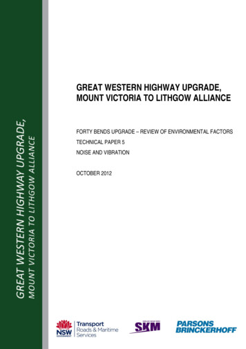
Low Noise, Low Drift, Low Power,3-Axis MEMS AccelerometersADXL356/ADXL357Data SheetFEATURESFUNCTIONAL BLOCK 1YOUTZVSSFigure 1. /SDAMISO/ASEL15429-002Hermetic package offers optimal long-term stability0 g offset vs. temperature (all axes): 0.75 mg/ C maximumUltralow noise spectral density (all axes): 75 μg/ HzLow power, VSUPPLY (LDO regulator enabled)ADXL356 in measurement mode: 150 μAADXL357 in measurement mode: 200 μAADXL356/ADXL357 in standby mode: 21 μAADXL356 has user adjustable analog output bandwidthADXL357 digital output featuresDigital SPI and limited I2C interfaces supported20-bit ADCData interpolation routine for synchronous samplingProgrammable high- and low-pass digital filtersIntegrated temperature sensorVoltage range optionsVSUPPLY with internal regulators: 2.25 V to 3.6 VV1P8ANA, V1P8DIG with internal LDO regulator bypassed: 1.8 Vtypical 10%Operating temperature range: 40 C to 125 C14-terminal, 6 mm 5.6 mm 2.2 mm, LCC packageFigure 2. ADXL357Inertial measurement units (IMUs)/attitude and headingreference systems (AHRSs)Platform stabilization systemsStructural health monitoringSeismic imagingTilt sensingRoboticsCondition monitoringGENERAL DESCRIPTIONThe analog output ADXL356 and the digital output ADXL357are low noise density, low 0 g offset drift, low power, 3-axisaccelerometers with selectable measurement ranges. TheADXL356B supports the 10 g and 20 g ranges, the ADXL356Csupports the 10 g and 40 g ranges, and the ADXL357 supportsthe 10 g, 20 g, and 40 g ranges.The ADXL356/ADXL357 offer industry leading noise, minimaloffset drift over temperature, and long-term stability, enablingprecision applications with minimal calibration.1The low drift, low noise, and low power ADXL357 enablesaccurate tilt measurement in an environment with highvibration. The low noise of the ADXL356 over higherfrequencies is ideal for condition-based monitoring and othervibration sensing applications.The ADXL357 multifunction pin names may be referenced onlyby their relevant function for either the serial peripheralinterface (SPI) or limited I2C interface.Protected by U.S. Patents 8,472,270; 9,041,462; 8,665,627; 8,917,099; 6,892,576; 9,297,825; and 7,956,621.Rev. ADocument FeedbackInformation furnished by Analog Devices is believed to be accurate and reliable. However, noresponsibility is assumed by Analog Devices for its use, nor for any infringements of patents or otherrights of third parties that may result from its use. Specifications subject to change without notice. Nolicense is granted by implication or otherwise under any patent or patent rights of Analog Devices.Trademarks and registered trademarks are the property of their respective owners.One Technology Way, P.O. Box 9106, Norwood, MA 02062-9106, U.S.A.Tel: 781.329.4700 2017–2020 Analog Devices, Inc. All rights reserved.Technical Supportwww.analog.com
ADXL356/ADXL357Data SheetTABLE OF CONTENTSFeatures . 1DRDY Pin . 29Applications . 1FIFO FULL. 29Functional Block Diagrams . 1FIFO OVR . 29General Description . 1Activity . 29Revision History . 3External Synchronization and Interpolation . 29Specifications. 4ADXL357 Register Map . 32Analog Output for the ADXL356 . 4Register Definitions. 33Digital Output for the ADXL357 . 5Analog Devices ID Register . 33SPI Digital Interface Characteristics for the ADXL357 . 7Analog Devices MEMS ID Register. 332I C Digital Interface Characteristics for the ADXL357 . 8Device ID Register . 33Absolute Maximum Ratings. 9Product Revision ID Register . 33Thermal Resistance . 9Status Register . 33Recommended Soldering Profile . 9FIFO Entries Register . 34ESD Caution . 9Temperature Data Registers . 34Pin Configurations and Function Descriptions . 10X-Axis Data Registers . 34Typical Performance Characteristics . 12Y-Axis Data Registers . 35Root Allan Variance (RAV) ADXL357 Characteristics . 20Z-Axis Data Registers . 35Theory of Operation . 21FIFO Access Register . 36Applications Information . 22X-Axis Offset Trim Registers . 36Analog Output . 22Y-Axis Offset Trim Registers . 36Digital Output . 22Z-Axis Offset Trim Registers . 37Axes of Acceleration Sensitivity . 23Activity Enable Register . 37Power Sequencing . 23Activity Threshold Registers . 37Power Supply Description . 23Activity Count Register . 37Overrange Protection. 23Filter Settings Register . 38Self Test . 23FIFO Samples Register . 38Filter . 24Interrupt Pin (INTx) Function Map Register. 38Serial Communications . 26Data Synchronization . 39SPI Protocol . 26I2C Speed, Interrupt Polarity, and Range Register . 39SPI Bus Sharing . 26Power Control Register . 39I2C Protocol . 27Self Test Register . 40Reading Acceleration or Temperature Data from the Interface. 27Reset Register . 40PCB Footprint Pattern . 41FIFO . 28Outline Dimensions . 42Interrupts . 29Ordering Guide . 42DATA RDY. 29Rev. A Page 2 of 42
Data SheetADXL356/ADXL357REVISION HISTORY6/2020—Rev. 0 to Rev. AChanges to Features Section, Applications Section, and GeneralDescription Section . 1Changes to Table 1 . 4Changes to Table 2 . 5Changes to Input Current Parameter, Table 3 . 7Changes to Acceleration (Any Axis, 0.1 ms) Parameter, Table 5;Thermal Resistance Section; and Table 6 . 9Moved Recommended Soldering Profile Section, Figure 5, andTable 7 . 9Changes to Table 8 .10Changes to Typical Performance Section and Figure 8 toFigure 13 .12Changes to Figure 14 to Figure 19 .13Changes to Figure 23 to Figure 25 .14Changes to Figure 32 to Figure 37 .16Changes to Figure 44 Caption, Figure 47 Caption, and Figure 48Caption .18Changes to Figure 50 Caption, Figure 52 Caption, andFigure 53 .19Changes to Theory of Operation Section .21Changes to Power Sequencing Section, V1P8ANA Section, andOverrange Protection Section .23Changes to Self Test Section, Filter Section, Figure 62, andFigure 63 .24Changes to Table 11 .25Changes to Serial Communications Section and Figure 64 .26Added SPI Bus Sharing Section and Figure 65; RenumberedSequentially .26Changes to I2C Protocol Section .27Changes to FIFO Section .28Changes to DRDY Pin Section, FIFO OVR Section, ActivitySection, NVM BUSY Section, and External Synchronizationand Interpolation Section . 29Changed EXT SYNC 00—No External Sync or InterpolationSection to EXT SYNC 00, EXT CLK 0—No ExternalSynchronization or Interpolation Section; EXT SYNC 10—External Sync with Interpolation Section to EXT SYNC 10,EXT CLK 0—External Synchronization with InterpolationSection; and EXT SYNC 01—External Sync and ExternalClock, No Interpolation Filter Section to EXT SYNC 01,EXT CLK 1—External Synchronization and External Clock,No Interpolation Filter Section . 30Changes to EXT SYNC 00, EXT CLK 0—No ExternalSynchronization or Interpolation Section, EXT SYNC 10,EXT CLK 0—External Synchronization with InterpolationSection, Table 13, and EXT SYNC 01, EXT CLK 1—External Synchronization and External Clock, No InterpolationFilter Section . 30Added EXT SYNC 10, EXT CLK 1—ExternalSynchronization and External Clock, with Interpolation FilterSection . 30Changes to Table 14 . 31Changes to Figure 74, Figure 75 Caption, and Figure 76 . 31Changes to Temperature Data Registers Section, Table 23,Table 24, and Table 25. 34Changes to Table 27, Table 28, Table 30 and Table 31 . 35Change to Table 42 Title . 37Changes to Table 44 . 38Changes to Reset Register Section . 40Changes to Figure 77 . 41Changes to Ordering Guide . 422/2017—Revision 0: Initial VersionRev. A Page 3 of 42
ADXL356/ADXL357Data SheetSPECIFICATIONSANALOG OUTPUT FOR THE ADXL356TA 25 C, VSUPPLY 3.3 V, x-axis acceleration and y-axis acceleration 0 g, z-axis acceleration 1 g, and full-scale range 10 g, unlessotherwise noted.Table 1.ParameterSENSOR INPUTOutput Full-Scale Range (FSR)Resonant Frequency1NonlinearityCross Axis SensitivitySENSITIVITYSensitivity at XOUT, YOUT, ZOUTSensitivity Change Due to TemperatureRepeatability20 g OFFSET0 g Output for XOUT, YOUT, ZOUT0 g Offset vs. Temperature (X-Axis, Y-Axis,and Z-Axis)3Repeatability2Vibration Rectification Error (VRE)4NOISESpectral Density5X-Axis, Y-Axis, and Z-AxisVelocity Random WalkX-Axis and Y-AxisZ-AxisBANDWIDTHSELF TESTOutput ChangeZ-AxisPOWER SUPPLYVoltage RangeVSUPPLY8VDDIOV1P8ANA, V1P8DIGCurrentMeasurement ModeVSUPPLYV1P8ANAV1P8DIGTest Conditions/CommentsEach axisADXL356B supports two rangesADXL356C supports two rangesMinMaxUnitggkHz% FSR% FSR% 10, 20 10, 405.50.11.31 10 g 40 gRatiometric to V1P8ANA 10 g 20 g 40 gTA 40 C to 125 CX-axis and y-axisZ-axisEach axis, 10 gReferred to V1P8ANA/2TA 40 C to 125 CTyp73.636.818.4804020 0.010.10.286.443.221.6mV/gmV/gmV/g%/ C%% 375 0.75 125 0.2 375 0.75mgmg/ CX-axis and y-axisZ-axisOffset due to 7.5 g rms vibration, 10 grange, in a 1 g orientation 4.25 5 0.1mgmgg 10 g 40 g 10 g75110μg/ Hzμg/ Hz38.226.5mm/sec/ Hrmm/sec/ HrkHz 3 dB, overall transfer function6 10 g range7Internal low dropout (LDO) regulatorbypassed, VSUPPLY 0 VLDO regulator enabledLDO regulator disabledLDO regulator disabledRev. A Page 4 of VVV15013812μAμAμA
Data SheetParameterStandby ModeVSUPPLYV1P8ANAV1P8DIGTurn On Time9OUTPUT AMPLIFIERSwingOutput Series ResistanceTEMPERATURE SENSOROutput at 25 CScale FactorTEMPERATUREOperating Temperature RangeADXL356/ADXL357Test Conditions/CommentsLDO regulator enabledLDO regulator disabledLDO regulator disabled10 g rangePower-off to standbyXOUT, YOUT, ZOUT, and TEMP pinsNo loadMinTypMaxUnit21710 10 100.03μAμAμAmsms32V1P8ANA 0.03VkΩ9673.0mVmV/ C 40 125 C1The resonant frequency is a sensor characteristic.Repeatability is predicted for a 10 year life and includes shifts due to the high temperature operating life (HTOL) (TA 150 C, VSUPPLY 3.6 V, and 1000 hours),temperature cycling ( 55 C to 125 C and 1000 cycles), velocity random walk, broadband noise, and temperature hysteresis. Repeatability in relation to time followsthe square root law. For example, to obtain offset repeatability of the x-axis for 2.5 years, use the following equation: 4.25 mg (2.5 years/10 years) 2.125 mg.3The temperature change is 40 C to 25 C, or 25 C to 125 C.4The VRE measurement is the shift in dc offset while the device is subject to 7.5 g rms of random vibration from 50 Hz to 2 kHz. The device under test (DUT) isconfigured for the 10 g range and an output data rate of 4 kHz. The VRE scales with the range setting.5Based on characterization.6Overall transfer function includes the sensor mechanical response and all other filters on the signal chain.7 10 g indicates a test condition. The self test result converted to the acceleration value is independent of the selected range.8When V1P8ANA and V1P8DIG are generated internally, VSUPPLY is valid. To disable the LDO regulator and drive V1P8ANA and V1P8DIG externally, connect VSUPPLY to VSS.9Standby to measurement mode. This specification is valid when the output is within 5 mg of the final value.2DIGITAL OUTPUT FOR THE ADXL357TA 25 C, VSUPPLY 3.3 V, x-axis acceleration and y-axis acceleration 0 g, z-axis acceleration 1 g, full-scale range 10 g, and outputdata rate (ODR) 500 Hz, unless otherwise noted. Note that multifunction pin names may be referenced only by their relevant function.Table 2.ParameterSENSOR INPUTOutput Full Scale Range (FSR)NonlinearityCross Axis SensitivitySENSITIVITY1X-Axis, Y-Axis, and Z-Axis SensitivityX-Axis, Y-Axis, and Z-Axis Scale FactorSensitivity Change due to TemperatureRepeatability20 g OFFSETX-Axis, Y-Axis, and Z-Axis 0 g Output0 g Offset vs. Temperature (X-Axis, Y-Axis, andZ-Axis)3Test Conditions/CommentsEach axisUser selectable, supports three rangesMinTA 40 C to 125 CRev. A Page 5 of 42Max 10, 20, 400.11.31 10 g 40 gEach axis 10 g 20 g 40 g 10 g 20 g 40 gTA 40 C to 125 CX-axis and y-axisZ-axisEach axis, 10 gTypUnitg% FSR% FSR%47,10423,55211,77651,20025,60012,80019.53978 μg/LSBμg/LSB%/ C%% 375 0.75 125 0.20 375 0.75mgmg/ C
ctral Density5X-Axis, Y-Axis, and Z-AxisVelocity Random WalkX-Axis and Y-AxisZ-AxisBANDWIDTH AND OUTPUT DATA RATEAnalog-to-Digital Converter (ADC) ResolutionLow-Pass Filter Passband FrequencyHigh-Pass Filter Passband Frequency WhenEnabled (Disabled by Default)SELF TESTOutput ChangeZ-AxisPOWER SUPPLYVoltage RangeVSUPPLY Operating7VDDIOV1P8ANA and V1P8DIGCurrentMeasurement ModeVSUPPLYV1P8ANAV1P8DIGStandby ModeVSUPPLYV1P8ANAV1P8DIGTurn On Time8Data SheetTest Conditions/CommentsX-axis and y-axisZ-axisOffset due to 7.5 g rms vibration, 10 grange, in a 1 g orientationMin 10 g 40 g 10 gTyp 4.25 5 0.1Max7590μg/ Hzμg/ Hz38.226.5mm/sec/ Hrmm/sec/ Hr20User programmable, Register 0x28User programmable, Register 0x28 for 4 kHzODR0.9770.0095 10 g range60.5Internal LDO regulator bypassed, VSUPPLY 0 2.51.83.63.61.98VVVLDO regulator enabledLDO regulator disabledLDO regulator disabled20016035.5μAμAμALDO regulator enabledLDO regulator disabledLDO regulator disabled 10 g rangePower-off to standby21710 10 10μAμAμAmsms1885 9.05LSBLSB/ CTEMPERATURE SENSOROutput at 25 CScale FactorTEMPERATUREOperating Temperature Range 401 125 CCharacterized but not 100% tested.Repeatability is predicted for a 10 year life and includes shifts due to the HTOL (TA 150 C, VSUPPLY 3.6 V, and 1000 hours), temperature cycling ( 55 C to 125 C and1000 cycles), velocity random walk, broadband noise, and temperature hysteresis. Repeatability in relation to time follows the square root law. For example, to obtainoffset repeatability of the x-axis for 2.5 years, use the following equation: 4.25 mg (2.5 years/10 years) 2.125 mg.3The temperature change is 40 C to 25 C or 25 C to 125 C.4The VRE measurement is the shift in dc offset while the device is subject to 7.5 g rms random vibration from 50 Hz to 2 kHz. The DUT is configured for the 10 g rangeand an output data rate of 4 kHz. The VRE scales with the range setting.5Based on characterization.6 10 g indicates a test condition. The self test result converted to the acceleration value is independent of the selected range.7When V1P8ANA and V1P8DIG are generated internally, VSUPPLY is valid. To disable the LDO regulator and drive V1P8ANA and V1P8DIG externally, connect VSUPPLY to VSS.8Standby to measurement mode. This specification is valid when the output is within 1 mg of final value.2Rev. A Page 6 of 42
Data SheetADXL356/ADXL357SPI DIGITAL INTERFACE CHARACTERISTICS FOR THE ADXL357Note that multifunction pin names may be referenced by their relevant function only.Table 3.ParameterDC INPUT LEVELSInput VoltageLow LevelHigh LevelInput CurrentLow LevelHigh LevelDC OUTPUT LEVELSOutput VoltageLow LevelHigh LevelOutput CurrentLow LevelHigh LevelAC INPUT LEVELSSCLK FrequencySCLK High TimeSCLK Low TimeCS Setup TimeCS Hold TimeCS Disable TimeRising SCLK Setup TimeMOSI Setup TimeMOSI Hold TimeAC OUTPUT LEVELSPropagation DelayEnable MISO TimeDisable MISO TimeSymbolTest Conditions/CommentsVILVIHMinTypMaxUnit0.3 VDDIOVV0.7 VDDIOIILIIHInput voltage (VIN) 0 VVIN VDDIOVOLVOHIOL IOL, MINIOH IOH, MAXIOLIOHVOL VOL, MAXVOH VOH, MIN 0.20.2 VDDIO0.8 VDDIO 100.14040202040202020Load capacitance (CLOAD) 30 Figure 3. SPI Interface Timing DiagramRev. A Page 7 of SμAμA0.2
ADXL356/ADXL357Data SheetI2C DIGITAL INTERFACE CHARACTERISTICS FOR THE ADXL357Note that multifunction pin names may be referenced only by their relevant function.Table 4.ParameterDC INPUT LEVELSInput VoltageLow LevelHigh LevelHysteresis of SchmittTriggered InputsInput CurrentDC OUTPUT LEVELSOutput VoltageLow LevelSymbolVILVIHVHYSIILVOL1VOL2Output CurrentLow LevelIOLAC INPUT LEVELSSCL FrequencySCL High TimeSCL Low TimeStart Setup TimeStart Hold TimeSDA Setup TimeSDA Hold TimeStop Setup TimeBus Free TimeSCL Input Rise TimeSCL Input Fall TimeSDA Input Rise TimeSDA Input Fall TimeWidth of Spikes toSuppressAC OUTPUT LEVELSPropagation DelayDataAcknowledgeOutput Fall TimeTest ATtSUSTOtBUFtRCLtFCLtRDAtFDAtSPMinI2C HS 0 (Fast Mode)Typ MaxI2C HS 1 (High Speed Mode)MinTypMax0.3 VDDIO0.7 VDDIO0.05 VDDIO0.1 VDDIO VIN 0.9 VDDIO0.3 VDDIO 10IOL 3 mAVDDIO 2 VVDDIO 2 VμA0.40.2 VDDIOVOL 0.4 VVOL 0.6 VVVV0.7 VDDIO0.1 VDDIO 102060.40.2 001603.412012012012050Not shown in Figure 4MHznsnsnsnsnsnsnsnsnsnsnsnsns808016016010CLOAD 500 pFtVDDATtVDACKtF97Not shown in Figure 445045012020 LOWtVDDATtHIGHtVDDATSCLFigure 4. I2C Interface Timing DiagramRev. A Page 8 of 42tFCLtRCLtVDACKtSUSTOtSUSTA15429-004tSUSTA tHDSTAUnit
Data SheetADXL356/ADXL357ABSOLUTE MAXIMUM RATINGSTable 5.RECOMMENDED SOLDERING PROFILERatingFigure 5 and Table 7 provide details about the recommendedsoldering profile.10,000 g10,000 g5.4 V1.98 VRAMP-UP 0.3 V to VDDIO 0.3 VtLTSMAXTSMINtSt25 C TO PEAKTIMEFigure 5. Recommended Soldering ProfileThermal performance is directly linked to printed circuit board(PCB) design and operating environment. Careful attention toPCB thermal design is required.θJA is the natural convection junction to ambient thermalresistance measured in a one cubic foot sealed enclosure. ψJB isthe junction to board thermal resistance.Table 7. Recommended Soldering ProfileProfile FeatureAverage Ramp Rate from LiquidTemperature (TL) to PeakTemperature (TP)PreheatMinimum Temperature(TSMIN)Maximum Temperature(TSMAX)Time from TSMIN to TSMAX (tS)TSMAX to TL Ramp-Up RateLiquid Temperature (TL)Time Maintained Above TL (tL)Table 6. Thermal ResistanceθJA42ψJB17.6RAMP-DOWNPREHEAT 40 C to 125 C 55 C to 150 CTHERMAL RESISTANCE1TL15429-005 0.3 V to VDDIO 0.3 V 0.3 V to V1P8ANA 0.3 VStresses at or above those listed under Absolute MaximumRatings may cause permanent damage to the product. This is astress rating only; functional operation of the product at theseor any other conditions above those indicated in the operationalsection of this specification is not implied. Operation beyondthe maximum operating conditions for extended periods mayaffect product reliability.Package TypeE-14-11CRITICAL ZONETL TO TPtPTPTEMPERATUREParameterAcceleration (Any Axis, 0.1 ms)UnpoweredPoweredVSUPPLY, VDDIOV1P8ANA, V1P8DIG Configured as InputsADXL356Digital Inputs (RANGE, ST1, ST2, STBY)Analog Outputs (XOUT, YOUT, ZOUT, TEMP)ADXL357Digital Pins (CS/SCL, SCLK/VSSIO,MOSI/SDA, MISO/ASEL, INT1, INT2,DRDY)Operating Temperature RangeStorage Temperature RangeUnit C/WPeak Temperature (TP)Thermal impedance simulated values are based on a JEDEC 2S2P thermaltest board with four thermal vias. See JEDEC JESD51.Time of Actual TP 5 C (tP)Ramp-Down RateTime from 25 C to PeakTemperature (t25 C TO PEAK)ESD CAUTIONRev. A Page 9 of 42ConditionSn63/Pb37Pb-Free3 C/sec3 C/secmaximummaximum100 C150 C150 C200 C60 sec to120 sec3 C/secmaximum183 C60 sec to150 sec240 C 0 C/ 5 C10 sec to30 sec6 C/secmaximum6 minutesmaximum60 sec to180 sec3 C/secmaximum217 C60 sec to150 sec260 C 0 C/ 5 C20 sec to40 sec6 C/secmaximum8 minutesmaximum
ADXL356/ADXL357Data Sheet12 XOUTY11 VSUPPLYRANGE 1ST1 2ADXL35610 V1P8ANAST2 3TOP VIEW(Not to Scale)9VSS8V1P8DIGXZSTBY 7VSSIO 6VDDIO 5TEMP 415429-00613 YOUT14 ZOUTPIN CONFIGURATIONS AND FUNCTION DESCRIPTIONSFigure 6. ADXL356 Pin ConfigurationTable 8. ADXL356 Pin Function DescriptionsPin iptionRange Selection Pin. Set this pin to ground to select the 10 g range, or set this pin to VDDIO to select the 20 g or 40 g range. This pin is model dependent (see the Ordering Guide section).Self Test Pin 1. This pin enables self test mode. This pin must be forced low when not in self test mode.Self Test Pin 2. This pin activates electromechanical self test actuation. This pin must be forced low when notin self test mode.Temperature Sensor Output.Digital Interface Supply Voltage.Digital Ground.Standby or Measurement Mode Selection Pin. Set this pin to ground to enter standby mode, or set this pinto VDDIO to enter measurement mode.Digital Supply. This pin requires a decoupling capacitor. If VSUPPLY connects to VSS, supply the voltage to thispin externally.Analog Ground.Analog Supply. This pin requires a decoupling capacitor. If VSUPPLY connects to VSS, supply the voltage to thispin externally.Supply Voltage. When VSUPPLY equals 2.25 V to 3.6 V, VSUPPLY enables the internal LDO regulators to generateV1P8DIG and V1P8ANA. For VSUPPLY VSS, V1P8DIG and V1P8ANA are externally supplied.X-Axis Output.Y-Axis Output.Z-Axis Output.Rev. A Page 10 of 42
12 INT1CS/SCL 111 VSUPPLYSCLK/VSSIO 2ADXL35710 V1P8ANAMOSI/SDA 3TOP VIEW(Not to Scale)9VSS8V1P8DIGXZRESERVED 7VSSIO 6VDDIO 5MISO/ASEL 4Y15429-00713 INT2ADXL356/ADXL35714 DRDYData SheetFigure 7. ADXL357 Pin Configuration (SPI/I2C)Table 9. ADXL357 Pin Function DescriptionsPin 21314INT1INT2DRDYDescriptionChip Select for SPI (CS).Serial Communications Clock for I2C (SCL).Serial Communications Clock for SPI (SCLK).I2C Mode Enable (VSSIO). Connect this pin to Pin 6 (VSSIO) to enable I2C mode.Master Output, Slave Input for SPI (MOSI).Serial Data for I2C (SDA).Master Input, Slave Output for SPI (MISO).Alternate I2C Address Select for I2C (ASEL).Digital Interface Supply Voltage.Digital Ground.Reserved. This pin can be connected to ground or left open.Digital Supply. This pin requires a decoupling capacitor. If VSUPPLY connects to VSS, supply the voltage to thispin externally.Analog Ground.Analog Supply. This pin requires a decoupling capacitor. If VSUPPLY connects to VSS, supply the voltage to thispin externally.Supply Voltage. When VSUPPLY equals 2.25 V to 3.6 V, VSUPPLY enables the internal LDO regulators to generateV1P8DIG and V1P8ANA. For VSUPPLY VSS, V1P8DIG and V1P8ANA are externally supplied.Interrupt Pin 1.Interrupt Pin 2.Data Ready Pin.Rev. A Page 11 of 42
ADXL356/ADXL357Data SheetTYPICAL PERFORMANCE CHARACTERISTICSAll figures include data for multiple devices and multiple lots, and they were taken in the 10 g range and TA 25 C, unless otherwise noted. ForFigure 52, the ODR is derived from a master clock, with a frequency of 1.024 MHz and 1.4% device to device variation (similar to ODR deviceto device variation). For a given device, however, clock frequency variation over the temperature range ( 40 C to 125 C) is no more than 1.2%, guaranteed by design.11001k10kFREQUENCY (Hz)0.01101001k10k0.10.01101001k10kFREQUENCY (Hz)Figure 9. ADXL356 Frequency Response for Y-Axis15429-012RELATIVE YOUT (g)115429-009RELATIVE YOUT (g)1FREQUENCY (Hz)Figure 12. ADXL357 Frequency Response for Y-Axis at 4 kHz ODR1RELATIVE ZOUT (g)1011001kFREQUENCY (Hz)10k15429-010RELATIVE ZOUT (g)10kFigure 11. ADXL357 Frequency Response for X-Axis at 4 kHz ODR100.1101kFREQUENCY (Hz)Figure 8. ADXL356 Frequency Resp
Data Sheet ADXL356/ADXL357 Rev. A Page 5 of 42 Parameter Test Conditions/Comments Min Typ Max Unit Standby Mode V SUPPLY LDO regulator enabled 21 μA V 1P8ANA LDO regulator disabled 7 μA V 1P8DIG LDO regulator disabled 10 μA Turn On Time9 10 g range 10 ms Power-off to standby 10 ms