Transcription
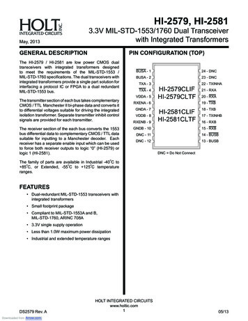
HI-2579, HI-2581May, 20133.3V MIL-STD-1553/1760 Dual Transceiverwith Integrated TransformersGENERAL DESCRIPTIONPIN CONFIGURATION (TOP)The HI-2579 / HI-2581 are low power CMOS dualtransceivers with integrated transformers designedto meet the requirements of the MIL-STD-1553 /MIL-STD-1760 specifications. The dual transceivers withintegrated transformers provide a single part solution forinterfacing a protocol IC or FPGA to a dual redundantMIL-STD-1553 bus.The transmitter section of each bus takes complementaryCMOS / TTL Manchester II bi-phase data and converts itto differential voltages suitable for driving the integratedisolation transformer. Separate transmitter inhibit controlsignals are provided for each transmitter.The receiver section of the each bus converts the 1553bus differential data to complementary CMOS / TTL datasuitable for inputting to a Manchester decoder. Eachreceiver has a separate enable input which can be usedto force both receiver outputs to logic “0” (HI-2579) orlogic 1 (HI-2581).BUSA - 124 - DNCBUSA - 223 - DNCTXA - 3TXA - 4VDDA - 5RXENA - 6GNDA - 7VDDB - 8RXENB - 9HI-2579CLIFHI-2579CLTFHI-2581CLIFHI-2581CLTFGNDB - 1022 - TXINHA21 - RXA20 - RXA19 - TXB18 - TXB17 - TXINHB16 - RXB15 - RXBDNC - 1114 - BUSBDNC - 1213 - BUSBDNC Do Not ConnectoThe family of parts are available in Industrial -40 C toooo 85 C, or Extended, -55 C to 125 C temperatureranges.FEATURES Dual-redundant MIL-STD-1553 transceivers withintegrated transformers Small footprint package Compliant to MIL-STD-1553A and B,MIL-STD-1760, ARINC 708A 3.3V single supply operation Less than 1.0W maximum power dissipation Industrial and extended temperature rangesDS2579 Rev. ADownloaded from Arrow.com.HOLT INTEGRATED CIRCUITSwww.holtic.com105/13
HI-2579, HI-2581BLOCK DIAGRAMVDDEach eControlBUSA/BNot UsedNot rComparatorRXENA/BGNDFigure 1. Block DiagramTXA/BTXA/BBUSA/B - BUSA/BVin(Line to Line)tDRtDRtDRRXA/B (HI-2579)tRGtRGtRGtRGRXA/B (HI-2579)RXA/B (HI-2581)RXA/B (HI-2581)Figure 2. Example WaveformsHOLT INTEGRATED CIRCUITS2Downloaded from Arrow.com.tDR
HI-2579, HI-2581PIN DESCRIPTIONSTable 1. Pin g O/PMIL-STD-1553 Bus A driver, negative signal (Transformer coupled or directcoupled bus connections)2BUSAAnalog O/PMIL-STD-1553 Bus A driver, positive signal (Transformer coupled or directcoupled bus connections)3TXADigital I/PTransmitter A digital data input, non-inverted4TXADigital I/PTransmitter A digital data input, inverted5VDDAPower6RXENADigital I/P7GNDAPowerTransceiver A ground connection8VDDBPowerTransceiver B 3.3V supply9RXENBDigital I/P10GNDBPower11DNC Not Used. Do Not Connect.12DNC Not Used. Do Not Connect.13BUSBAnalog O/PMIL-STD-1553 Bus B driver, positive signal (Transformer coupled or directcoupled bus connections)14BUSBAnalog O/PMIL-STD-1553 Bus B driver, negative signal (Transformer coupled or directcoupled bus connections)15RXBDigital I/PReceiver B output, inverted16RXBDigital I/PReceiver B output, non-inverted17TXINHBDigital I/PTransmit inhibit, Bus B. If high BUSB, BUSB outputs are disabled18TXBDigital I/PTransmitter B digital data input, non-inverted19TXBPowerTransmitter B digital data input, inverted20RXAPowerReceiver A output, inverted21RXADigital I/PReceiver A output, non-inverted22TXINHADigital I/PTransmit inhibit, Bus A. If high BUSA, BUSA outputs are disabled23DNC Not Used. Do Not Connect.24DNC Not Used. Do Not Connect.Transceiver A 3.3V supplyReceiver A enable. If low, forces both RXA and RXA low (HI-2579) or High(HI-2581)Receiver B enable. If low, forces both RXB and RXB low (HI-2579) or High(HI-2581)Transceiver B ground connectionHOLT INTEGRATED CIRCUITS3Downloaded from Arrow.com.
HI-2579, HI-2581FUNCTIONAL DESCRIPTIONThe HI-2579 family of data bus transceivers containsdifferential voltage source drivers, differential receiversand integrated transformers. They are intended forapplications using a MIL-STD-1553 A/B data bus.Transmitterthreshold comparator that produces CMOS data at theRXA/B and RXA/B output pins. When the MIL-STD-1553bus is idle and RXENA or RXENB are high, RXA/B willbe logic “0” on HI-2579 and logic “1” on HI-2581.Each set of receiver outputs can also be independentlyforced to the bus idle state (logic “0” on HI-2579 or logic“1” on HI-2581) by setting RXENA or RXENB low.Data is input to the device’s transmitter section fromthe complementary CMOS inputs TXA/B and TXA/B.The transmitter accepts Manchester II bi-phase dataand converts it to differential voltages which drive theinternal transformers on BUSA/B and BUSA/B. Thetransformer outputs are either direct or transformercoupled to the MIL-STD-1553 data bus. Both couplingmethods produce a nominal voltage on the main bus of7.5 volts peak to peak.MIL-STD-1553 Bus InterfaceThe transmitter is automatically inhibited and placed inthe high impedance state when both TXA/B and TXA/Bare either at a logic “1” or logic “0” simultaneously. A logic“1” applied to the TXINHA/B input forces the transmitterto the high impedance state, regardless of the state ofTXA/B and TXA/B.ReceiverIn a transformer coupled interface, the transceiver isconnected to the internal 1:2.5 isolation transformerwhich in turn is connected to a 1:1.4 coupling transformer.The transformer coupled method also requires twocoupling resistors equal to 75% of the bus characteristicimpedance (Zo) between the coupling transformer andthe bus. The coupling transformer and coupling resistorsare commonly integrated in a single device known as astub coupler.The receiver accepts bi-phase differential data fromthe MIL-STD-1553 bus through the same direct ortransformer coupled interface as the transmitter. Thereceiver’s differential input stage includes a filter andFigure 4 and Figure 5 show test circuits for measuringelectrical characteristics of both direct and transformercoupled interfaces respectively (see “electricalcharacteristics” on the following pages) .ABSOLUTE MAXIMUM RATINGSRECOMMENDED OPERATINGCONDITIONSSupply voltage (VDD)Logic input voltage range-0.3 V to 5 V-0.3 V DC to 3.6 VReceiver differential voltage50 Vp-pDriver peak output current 1.0 APower dissipation at 25 C1.0 WSolder TemperatureJunction TemperatureStorage Temperature245 C max.ooA direct coupled interface uses the internal 1:2.5 ratioisolation transformer and two 55Ω isolation resistorsbetween the transformer and the bus.Supply Voltageo-65 C to 150 CooIndustrial Screening-40 C to 85 CHi-Temp Screening-55 C to 125 CooNOTE: Stresses above absolute maximum ratings or outsiderecommended operating conditions may cause permanentdamage to the device. These are stress ratings only. Operationat the limits is not recommended.HOLT INTEGRATED CIRCUITS4Downloaded from Arrow.com.VDD 3.3V 5%Temperature Rangeo175 CThere are two ways of connecting to the MIL-STD-1553bus, using a direct coupled interface or a transformercoupled interface (see Figure 3).
HI-2579, HI-2581ELECTRICAL CHARACTERISTICSTable 2. DC Electrical CharacteristicsVDD 3.3V, GND 0V, TA Operating Temperature Range (unless otherwise stated)ParameterSymbolOperating VoltageTest ConditionsVDDMinTypMaxUnits3.153.33.45VICC1Not Transmitting417mAICC2Transmit one bus @ 50%duty cycle225320mAICC3Transmit one bus @ 100%duty cycle425640mAPD1Not Transmitting0.06WPD2Transmit one bus @ 100%duty cycle1.0WMin. Input Voltage (HI)VIHDigital InputsMax. Input Voltage (LO)VILDigital Inputs30%VDDMin. Input Current (HI)IIHDigital Inputs20μAMax. Input Current (LO)IILDigital Inputs-20μAVOHIOUT -1.0mA, Digital Outputs90%VDDVOLIOUT 1.0mA, DigitalOutputsTotal Supply CurrentPower DissipationMin. Output Voltage (HI)Max. Output Voltage (LO)RECEIVER70%VDD10%VDD(Measured at Point “AD” in Figure 2 unless otherwise specified)Input ResistanceRINDifferentialInput CapacitanceCINDifferentialCommon Mode Rejection RatioInput Common Mode VoltageThreshold Voltage - DirectCoupledThreshold Voltage - TransformerCoupled245VICM-10.0DetectVTHDNo DetectVTHNDDetectVTHDNo DetectVTHNDkΩ5CMRR1MHz Sine Wave(measured at point “AD” inFigure 4)0.861MHz Sine Wave(measured at point “AT” inFigure 5)0.86HOLT INTEGRATED CIRCUITS5Downloaded from Arrow.com.0.5pFdB 10.0V-pkVp-p0.28Vp-pVp-p0.20Vp-p
HI-2579, HI-2581ParameterSymbolTest ConditionsMinTypMaxUnitsTRANSMITTER (Measured at Point “AD” in Figure 2 unless otherwise specified)Output VoltageDirectCoupledVOUT35Ω Load (measured atpoint “AD” in Figure 4)6.19.0Vp-pTransformerCoupledVOUT70Ω Load (measured atpoint “AT” in Figure 5)20.027.0Vp-pVONDifferential, Inhibited10mVp-pDirectCoupledVDYN35Ω Load (measured atpoint “AD” in Figure 4)-90 90mVTransformerCoupledVDYN70Ω Load (measured atpoint “AT” in Figure 5)-250 250mVCOUT1MHz Sine Wave15pFMaxUnitsOutput NoiseOutput Dynamic Offset VoltageOutput CapacitanceTable 3. AC Electrical CharacteristicsVDD 3.3V, GND 0V, TA Operating Temperature Range (unless otherwise stated)ParameterSymbolTest ConditionsMinTypRECEIVER (Measured at Point “AT” in Figure 3)Receiver DelaytDRFrom input zero crossing toRXA/B or RXA/BReceiver Gap TimetRGSpacing between RXA/Band RXA/B pulsesReceiver Enable DelaytRENFrom RXENA/B rising orfalling edge to RXA/B orRXA/B40ns150ns450Note 390Note 1365Note 3nsnsTRANSMITTER (Measured at Point “AD” in Figure 2)Driver DelaytDTTXA/B, TXA/B to BUSA/B,BUSA/BRise Timetr35Ω Load100300nsFall Timetf35Ω Load100300nstDI-HInhibited Output100nstDI-LActive Output150nsInhibit DelayNote 1. Measured using a 1 MHz sinusoid, 20 V peak to peak, line to line at point “AT” (Guaranteed but not tested).Note 2. Measured using a 1 MHz sinusoid, 860 mV peak to peak, line to line at point “AT” (100% tested).Note 3. Measured using a 1 MHz sinusoid, 860 mV peak to peak, line to line at point “AT”. Measured from input zero crossing point.HOLT INTEGRATED CIRCUITS6Downloaded from Arrow.com.
HI-2579, HI-2581MIL-STD-1553BUS A(Direct sceiver AMIL-STD-1553BUS B(Transformer Coupled)1:2.5MIL-STD-1553Stub CouplerIsolationTransformer52.5ΩBUSBTransceiver BBUSB52.5Ω1:2.51:1.4HI-2579Figure 3. Bus Connections Example using HI-2579VDDIsolationTransformerTXA/BTXA/BRXA/BEach A/B55ΩHI-2579Point“AD”GNDFigure 4. Direct Coupled Test CircuitVDDIsolationTransformerTXA/BTXA/BRXA/BEach -2579GNDFigure 5. Transformer Coupled Test CircuitHOLT INTEGRATED CIRCUITS7Downloaded from Arrow.com.Point“AT”
HI-2579, HI-2581ORDERING INFORMATIONHI - 25xx CL x FPART NUMBERLEAD FINISHFPb-free, RoHS compliantPART NUMBERTEMPERATURE RANGELEADFINISHI-40oC to 85oCIGoldT-55oC to 125oCTGoldPART NUMBERRXENA 0RXENB 0RXARXARXBRXB2579000025811111HOLT INTEGRATED CIRCUITS8Downloaded from Arrow.com.FLOW
HI-2579, HI-2581REVISION HISTORYRevisionDS2579,DateDescription of ChangeRev. New10/8/12Initial ReleaseRev. A5/23/13Correct Note 1 on package dimensions to state that the Heatsink pad is connectedinternally to ground.HOLT INTEGRATED CIRCUITS9Downloaded from Arrow.com.
HI-2579, HI-2581PACKAGE DIMENSIONSBottom ViewDimensions in inches (mm).660 .007(16.76 .18).218(5.54).060 TYP.(1.52)R.017 24X(R.43)23X .050(1.27)24XR.008(R.20)PIN 1 INDEX.510 .007(12.95 44 SQ. 6X(1.12 SQ.).600 .007(15.24 .18)Notes:1.Heatsink pad is internally connected to device GND pins. Connection to external GND for heat extraction is not necessary.2.The “keep out” zones (crosshatched) enclose test pads for the transformer primary windings. DO NOT CONNECT.3.Routing traces under test pads is not recommended.HOLT INTEGRATED CIRCUITS10Downloaded from Arrow.com.
HI-2579, HI-2581PACKAGE DIMENSIONSTop ViewDimensions in inches (mm).440 .015(11.18 .38).800 .015(20.32 .38).005 max.(.13).370 .011(9.40 .28).300 .005(7.62 .13)PIN 1 INDEXIN TOPMARK.004(.10).070 .007(1.78 .18)HOLT INTEGRATED CIRCUITS11Downloaded from Arrow.com.
10 GNDB Power Transceiver B ground connection 11 DNC í Not Used. Do Not Connect. 12 DNC í Not Used. Do Not Connect. 13 BUSB Analog O/P MIL-STD-1553 Bus B driver, positive signal (Transformer coupled or direct coupled bus connections) 14 BUSB Analog O/P MIL-STD-1553 Bus B driver, negative signal (Transformer coupled or direct coupled bus .