Transcription
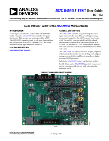
ADZS-U4050LF-EZKIT User GuideUG-1163One Technology Way P.O. Box 9106 Norwood, MA 02062-9106, U.S.A. Tel: 781.329.4700 Fax: 781.461.3113 www.analog.comADZS-U4050LF-EZKIT for the ADuCM4050 MicrocontrollerINTRODUCTIONGENERAL DESCRIPTIONThis user guide describes the ADZS-U4050LF-EZKIT that isused to evaluate the ADuCM4050 microcontroller. This guidedescribes the different parts and components of the ADZSU4050LF-EZKIT evaluation board, as well as the functionalitiesand configurations of the ADZS-U4050LF-EZKIT that enablethe user to develop applications with the device.The ADuCM4050 is an ultra low power, integrated, mixedsignal microcontroller units (MCUs) used for processing,control, and connectivity. The MCU system is based on anARM Cortex-M4F processor, which is a 32-bit reducedinstruction set computer (RISC) processor and runs up to52 MHz. The device has 512 kB of embedded flash memorywith error correction code (ECC) and 128 kB of system RAMwith parity.DOCUMENTS NEEDEDADuCM4050 EZ-Kit ManualThe ADuCM4050 also features a collection of digital peripherals,and an analog subsystem that provides clocking, reset, and powermanagement capabilities in addition to an analog-to-digitalconverter (ADC) subsystem.Refer to the ADuCM4050 product page for future updates.For full details, see the ADuCM4050 data sheet, which must beused in conjunction with this user guide when using theevaluation board.16076-001EVALUATION BOARD PHOTOGRAPHFigure 1.PLEASE SEE THE LAST PAGE FOR AN IMPORTANTWARNING AND LEGAL TERMS AND CONDITIONS.Rev. 0 Page 1 of 31
UG-1163ADZS-U4050LF-EZKIT User GuideTABLE OF CONTENTSIntroduction . 1Documents Needed . 1On-Board Trisensor Circuit (Accelerometer, Temperature,and ADC) .8General Description . 1On-Board Digital I2C Temperature Sensor .9Evaluation Board Photograph. 1On-Board 32 Mb Serial Flash Memory. 10Revision History . 2On-Board Buzzer . 10Overview . 3ADZS-U4050LF-EZKIT Board Connectors . 11Contents . 3Arduino UNO Connectors (J4, J5, J6, and J7) . 11J-Link LITE Emulator . 3Expansion Interface 3 (EI3) . 14Board Features . 4Wireless Tranceivers Interface (P1, P2, and P3) . 15Power Supply. 4Emulation and Serial Interface Connector (P4, P5, and P9) 15Power Indicator/General-Purpose LEDs . 5ADZS-U4050LF-EZKIT Board System Architecture . 16Crystal Circuits . 5Evaluation Board Schematics and Artwork . 17Emulator Interface . 5Ordering Information . 29Reset, Wake, Boot, and General-Purpose Push-Buttons . 6Bill of Materials . 29USB to UART Interface . 7mbed Interface . 7REVISION HISTORY5/2018—Revision 0: Initial VersionRev. 0 Page 2 of 31
ADZS-U4050LF-EZKIT User GuideUG-1163The ADZS-U4050LF-EZKIT allows the user to program, debug,and evaluate the performance of the ADuCM4050microcontroller.The serial wire debug connector is a 20-pin device, but onlythree connections are made: SWDIO and SWCLK are used fordebug purposes and the RESET connection is used to provide areset from the PC if required. Table 1 shows the JTAG connectorpin configuration.CONTENTSTable 1. JTAG Connector PinoutsThe ADZS-U4050LF-EZKIT package contains the followingitems (see Figure 2):Pin Number14, 6, 8, 10, 12, 14, 16, 18, 207915OVERVIEW ADZS-U4050LF-EZKIT boardUSB 2.0 cableJ-Link LITE emulatorJ-Link LITE EmulatorWhen measuring current consumption using an external supplyon the ADZS-U4050LF-EZKIT board IOVDD pins, it is recommended that the emulator be disconnected.The connection on the board is used in P4 a debug port.16076-002The J-Link LITE emulator board provides a debug path interfacevia serial wire, power supply, and UART communication withthe ADZS-U4050LF-EZKIT board. Figure 3 shows a top view ofthe emulator board.SignalVDDGNDSWDIOSWCLKRESETFigure 2. ADZS-U4050LF-EZKIT Package ContentsRev. 0 Page 3 of 31
ADZS-U4050LF-EZKIT User Guide16076-003UG-1163Figure 3. J-Link LITE Emulator BOARD FEATURESPower SupplyThe ADZS-U4050LF-EZKIT evaluation board can be poweredby numerous sources to evaluate the capability of theADuCM4050 microcontroller. The following sources are the options for powering the board: External power supply. The ADZS-U4050LF-EZKIT boardpackage has a 5 V dc regulated power adapter included. Touse the adapter to supply the microcontroller, Pin 3 andPin 5 of JP12, and Pin 1 and Pin 3 of JP14 must be shorted;then, connect the adapter to the P8 power jack.J-Link LITE emulator. The J-Link LITE emulator can powerthe evaluation board while debugging and programmingthe microcontroller. Pin 1 and Pin 3 of JP12 and Pin 1 andPin 3 of JP14 must be shorted to use this option. To powerthe board by this option, the user must also command theJ-Link LITE to power on the board. Run the J-Link LITEcommander, and then execute the power on permcommand. USB power supply. The ADZS-U4050LF-EZKIT board candraw power from the USB to the UART port on the lowerright side of the board. The configuration for this setup isshorting Pin 3 and Pin 4 of JP12 and Pin 1 and Pin 3 of JP14.USB mbed. The ADZS-U4050LF-EZKIT board can drawpower from the USB to the mbed interface on the lowerside of the board. The jumper configuration is the same asthe previous one.Coin cell battery. The ADZS-U4050LF-EZKIT board can bepowered by a 3 V coin cell battery (included in the kit). Touse the coin cell battery, Pin 1 and Pin 2 of JP16 and Pin 3and Pin 4 of JP14 must be shorted.AA battery. To use an AA battery, Pin 2 and Pin 3 of JP16and Pin 3 and Pin 4 of JP14 must be shorted.Photovoltaic (PV) cell. The ADZS-U4050LF-EZKIT boardcan be also be powered by energy harvesting kits providedby Analog Devices, Inc. To use this option, Pin 3 and Pin 5of JP14 must be shorted.The configurations for the power options are listed in Table 2.The pin numbers indicate the pins to be shorted.Rev. 0 Page 4 of 31
ADZS-U4050LF-EZKIT User GuideUG-1163Table 2. Power Option Configurations of the ADZS-U4050LF-EZKIT Board1Pin NumberJP141, 31, 31, 31, 33, 43, 43, 5JP1213, 51, 33, 43, 4XXXSourceExternal Power AdapterEmulator/J-Link LITEUSB PowerUSB mbedCoin Cell BatteryAA BatteryPV CellJP161XXXX1, 22, 3XX means don’t careThe 5 V sources (external power, emulator, and USBs) areconnected to the on-board 3.0 V low dropout regulator (LDO)before they power the components and the microcontroller onthe board.The battery and the PV cell supplies are directly connected tothe ADZS-U4050LF-EZKIT internal components (microcontroller,flash, temperature sensor, and accelerometer). Do not supplymore than 3.6 V on the battery and PV cell terminals to avoiddamaging the microcontroller.Power Indicator/General-Purpose LEDsThe ADZS-U4050LF-EZKIT board has seven LEDs to indicatedifferent board statuses. LED1 (red) indicates if the board hasbeen reset. LED2 (green) indicates that the board is powered up.LED7 (yellow) indicates mbed enabled.The general-purpose yellow LEDs (LED3, LED4, and LED5) areprogrammable and connected to the pins of the microcontroller.These are all active low LEDs; this means that writing low to thepins where the LED is connected lights up the LEDs.The red, green, blue (RGB) LED (LED6) is a multicolor LED,which internally uses three monocolor LEDs, one per primarycolor, to combine the lights and create new colors. The monocolorLEDs can be controlled independently from the microcontroller.JP9 must be closed.Table 3. LED to MCU Pin ConnectionsLED No.LED1LED2LED3LED4LED5LED6LED7Pin No.SYS HWRSTNot applicable, LED2 is directly connected to thepower lineP0 13P1 12P1 13P1 06, P1 07, P1 08Not applicable (LED7 is controlled by mbed circuit)Crystal CircuitsThe ADZS-U4050LF-EZKIT board uses two crystals to clock thesystem: a 26 MHz and a 32.768 kHz crystal. The 26 MHz crystal isa possible clock source for the full system such as the core, SRAM,bus, flash, and others. The 32.768 kHz crystal is a possible clocksource of the low frequency multiplexer (LFMUX) block, connected to the low speed peripherals, such as the beeper controlleror timers.Emulator InterfaceApplication, download, and emulation are possible on theADuCM4050 via a serial wire by using the J-Link LITE emulatorthrough the P4 connector of the ADZS-U4050LF-EZKIT board.The LED to MCU pin connections are described in Table 3.Rev. 0 Page 5 of 31
UG-1163ADZS-U4050LF-EZKIT User GuideReset, Wake, Boot, and General-Purpose Push-Buttons The ADZS-U4050LF-EZKIT board has five push-buttons (seeFigure 4) responsible for different operations. The boot mode select switch (SW1) determines the bootmode of the processor. By default, the processor bootsfrom the internal flash memory. When pressed, the UARTdownload mode is triggered. For full details, see theADuCM4050 EZ-Kit Manual, Revision 1.0 for furtherinformation, which can be found in the Documentationsection of the ADuCM4050 product page (this manual isincluded in the downloadable board support package fortheADuCM4050).The reset switch (SW2) resets the ADuCM4050 processor.The wake switch (SW3) is connected to the processor wakesignals, and is used to wake up the processor during lowpower modes. Depending on the configuration of JP10, thedifferent external interrupts to wake up themicrocontroller. Table 4. External Interrupt Choice for the WAKE SwitchPin Number1, 23, 45, 67, 8Signal NameSYS WAKE0SYS WAKE1SYS WAKE2SYS WAKE316076-004 The PB1 switch (SW4) is a general-purpose switch connectedto general-purpose input/output (GPIO) P2 09.The PB2 switch (SW5) is a general-purpose switch connectedto GPIO P2 06.Table 4 shows which pins must be shorted on JP10 to choosewhich external interrupt is connected to the WAKE switch.The PB1 switch (SW4) is a general-purpose switch connectedto general-purpose input/output (GPIO) P2 09.The PB2 switch (SW5) is a general-purpose switch connectedto GPIO P2 06.Figure 4. ADZS-U4050LF-EZKIT Push-Buttons Located Near the LEDsRev. 0 Page 6 of 31
ADZS-U4050LF-EZKIT User GuideUG-1163USB to UART Interfacembed InterfaceThe ADZS-U4050LF-EZKIT has an on-board USB to UARTinterface circuit used to connect the ADuCM4050 microcontrollers to a PC. The USB to UART functionality is provided byan FT232RQ (U4) chip. The chip handles the entire USB protocolon-chip and no USB firmware development is required. TheFT232RQ can transfer data at rates from 300 baud to 3 Mbaud attransistor to transistor (TTL) levels.mbed is a platform based on Cortex-M that features severalcomponents including an operating system and protocols. Oneof these components is the programming interface CMSIS-DAPcompliant.16076-005The ADuCM4050 microcontroller UART0 pins are connecteddirectly to the interface pins of the FT232RQ chip (U4). If anotherUSB to UART module is used, the UART1 signals can be tappedon the P7 4 1 header.The ADZS-U4050LF-EZKIT board has a programming interface,which enables the device to be programmed and debugged viaUSB. When connected to a PC, an external unit called DAPLINKand a new COM port appears; if not, installing the mbedWindows serial port driver is required. For further information,see the ARM mbed web page.Figure 5. USB to UART Circuit (Right) and USB to mbed Circuit (Left)Rev. 0 Page 7 of 31
UG-1163ADZS-U4050LF-EZKIT User GuideOn-Board Trisensor Circuit (Accelerometer, Temperature, and ADC)The ADZS-U4050LF-EZKIT board has an on-board trisensorcircuit consisting of a 3-axis micro electromechanical systems(MEMS) accelerometer, a temperature sensor, and an ADC,which is provided by the ADXL363 (U2), shown in Figure 6.This circuit can be powered down by unshorting the JP6 header.16076-006The entire system consumes less than 2 μA at a 100 Hz outputdata rate and 270 nA that, when in motion, triggers the wakeup mode. The ADXL363 communicates with the ADuCM4050microcontroller via the serial port interface (SPI2). The accelerometer provides selectable measurements of 2G, 4G, and 8Gwith a resolution of 1 mG per least significant bit (LSB) on the 2Grange. The temperature sensor operates with a scale factor of0.065 C. The ADC has no external connections, but can be usedby tapping to the TP8 test point.Figure 6. Trisensor CircuitRev. 0 Page 8 of 31
ADZS-U4050LF-EZKIT User GuideUG-1163On-Board Digital I2C Temperature Sensor2The ADZS-U4050LF-EZKIT board has an on-board I C digitaltemperature sensor, ADT7420. The ADT7420 (U6) is rated foroperation over the 40 C to 150 C temperature range.The ADT7420 operates from 2.7 V to 5.5 V. Operating at 3.3 V,the average supply current is typically 210 μA and the shutdowncurrent is typically 2.0 μA.The ADT7420 is connected to the I2C interface and can generatean interrupt signal to interrupt the microcontroller. The interruptsignal pin of the ADT7420 is connected to Pin P1 14 of theADuCM4050.The temperature sensor can be disconnected from the boardsupply by unshorting the JP5 header. Figure 7 shows the circuitwith the ADT7420 chip in the middle and the JP5 header abovethe chip.16076-007The ADT7420 has two available pins for address selection withfour possible I2C addresses. The user can configure the addressby soldering resistors in R39 and R40 (to VCC), and R41 andR42 (to GND). The default address is 0x48.Figure 7. I2C Temperature CircuitRev. 0 Page 9 of 31
UG-1163ADZS-U4050LF-EZKIT User GuideOn-Board 32 Mb Serial Flash MemoryThe ADZS-U4050LF-EZKIT board has an on-board, serial flashmemory that can be used to store voice, text, and data.On-Board BuzzerThe ADZS-U4050LF-EZKIT has a buzzer (D1) thatgenerates tones and alarms with the beeper controller insidethe ADuCM4050 microcontroller. Figure 9 shows the buzzerchip next to the PV cell connector.16076-008The serial flash memory (U7) is a W25Q32 chip that has a storagesize of 32 Mb. This chip supports a standard serial peripheralinterface (SPI) with speeds up to 104 MHz. The chip is interfacedwith the SPI2 of the microcontroller and can be disconnected tothe board by unshorting the JP4 header.Figure 8 shows the circuit with the W25Q32 chip in the middleand the JP4 header below the flash chip.16076-009Figure 8. External 32 Mb Serial Flash MemoryFigure 9. Buzzer CircuitRev. 0 Page 10 of 31
ADZS-U4050LF-EZKIT User GuideUG-1163ADZS-U4050LF-EZKIT BOARD CONNECTORSThe ADZS-U4050LF-EZKIT board has a number of connectorsused to connect different boards and kits for evaluation. Thelocations of these connectors are shown in Figure 10.ARDUINO UNO CONNECTORS (J4, J5, J6, AND J7)The ADZS-U4050LF-EZKIT board has an Arduino Unocompatible form factor interface that can accept Arduinoshields and daughter boards. The pinout of the Arduinointerface is described in Table 5 through Table 8.Table 5. Arduino Interface J4 Connector PinoutJ4 Pin No.12345678Arduino Pin NameNo connect3VRST3V5VGNDGNDVINADuCM4050 Pin NameNot applicableNot applicableSYS HWRSTNot applicableNot applicableNot applicableNot applicableNot applicableTable 6. Arduino Interface J5 Connector PinoutArduino Pin NameA0A1A2A3A4A5Not applicableNot applicableADuCM4050 Pin NameADC0 VIN0 (P2 03)ADC0 VIN1 (P2 04)ADC0 VIN2 (P2 05)ADC0 VIN3 (P2 06)ADC0 VIN4 (P2 07)ADC0 VIN5 (P2 08)P1 03/GPIO19/SPI2 MOSIP1 04/GPIO20/SPI2 MISO16076-010J5 Pin No.12345678Figure 10. Connector LocationsRev. 0 Page 11 of 31
UG-1163ADZS-U4050LF-EZKIT User GuideTable 7. Arduino Interface J6 Connector PinoutJ6 Pin No.12345678Arduino Pin No.01234567ADuCM4050 Pin NameP0 11/UART0 RXP0 10/UART0 TXP0 15/GPIO15/SYS WAKE0P2 11/GPIO43/SP1 CS1/SYS CLKOUT/RTC1 OPC1P2 01/GPIO33/SYS WAKE3/TMR2 OUTP2 02/GPIO34/SPT0 ACN/SPI1 CS2P2 00/GPIO32/SPT0 AFS/UART1 RXP0 12/GPIO12/SPT0 AD0Table 8. Arduino Interface J7 Connector PinoutADuCM4050 Pin NameP1 02/GPIO18/SPI2 CLKP1 15/GPIO31/SPT0 ACLK/UART1 TXP0 03/GPIO03/SPI0 CS0/SPT0 BCNV/SPI2 RDYP0 01/GPIO01/SPI0 MOSI/SPT0 BFSP0 02/GPIO02/SPI0 MISO/SPT0 BD0P0 00/GPIO00/SPI0 CLK/SPT0 BCLKGNDVREF ADCP0 05/I2C0 SDAP0 04/I2C0 SCL16076-011Arduino Pin Name8910111213GNDAREFSDASCLFigure 11. J4 and J5 Arduino Compatible Interface (Power and ADC)16076-012J7 Pin No.12345678910Figure 12. J6 Arduino Compatible Interface (GPIO)Rev. 0 Page 12 of 31
UG-116316076-013ADZS-U4050LF-EZKIT User GuideFigure 13. J7 Arduino Header (GPIO Pins, SPI, and I2C)Rev. 0 Page 13 of 31
UG-1163ADZS-U4050LF-EZKIT User GuideEXPANSION INTERFACE 3 (EI3)An EI3 SDP breakout board (sold separately), as shown inFigure 15, is required to tap and probe the signals in thisconnector.16076-014The ADZS-U4050LF-EZKIT board includes one expansioninterface connector located on the bottom side of the board. EI3supports connection to other EI3 daughter boards designed byAnalog Devices, extending the capabilities of the evaluationboard. The connectors provide power, ground, reset, ADC, I2C,SPI, UART, serial port (SPORT), and GPIO signals.16076-015Figure 14. EI3 ConnectorFigure 15. EI3 SDP Breakout Board Connected to the ADZS-U4050LF-EZKIT BoardRev. 0 Page 14 of 31
ADZS-U4050LF-EZKIT User GuideUG-1163WIRELESS TRANCEIVERS INTERFACE (P1, P2,AND P3)EMULATION AND SERIAL INTERFACE CONNECTOR(P4, P5, AND P9)The wireless transceiver daughterboard interface supports theADF7023, ADF7024, ADF7242, ADF7030, and ADF7030-1wireless transceivers. These are low power, high performance,integrated radio transceivers supporting a wide range of modulation schemes and channel widths in the sub GHz and2.4 GHz frequency ranges.The P4, P5, and P9 connectors provide a connection from theADZS-U4050LF-EZKIT board to the emulator board. P4 is a20-pin standard JTAG connector compatible with the J-LinkLITE emulator.16076-017P5 and P9 are 10-pin debug/emulator connectors with serialwire, power source, and UART signal lines for debuggingpurposes.16076-018Figure 16. P9 Debug ConnectorFigure 17. P4 and P5 Debug ConnectorsRev. 0 Page 15 of 31
UG-1163ADZS-U4050LF-EZKIT User GuideADZS-U4050LF-EZKIT BOARD SYSTEM ARCHITECTUREFigure 18 shows a block diagram of the ADZS-U4050LF-EZKIT board.32 Mb PIN 0.05"SWD20-PIN 0.10"mbedPBs (2)I2C0SPI2GPIOLEDs 0ADCSPORT ALLJ-LINKE13 (1A)ADP53013.3VFigure 18. ADZS-U4050LF-EZKIT Board Block DiagramRev. 0 Page 16 of 3116076-019USBADXL363
ADZS-U4050LF-EZKIT User GuideUG-1163EVALUATION BOARD SCHEMATICS AND ARTWORKFigure 19 through Figure 37 show the schematics of the ADZS-U4050LF-EZKIT board.P2 00/GPIO32/SPT0 AFS/UART1 RXP0 00/GPIO00/SPI0 CLK/SPT0 BCLKP2 01/GPIO33/SYS WAKE3/TMR2 OUTP0 01/GPIO01/SPI0 MOSI/SPT0 BFSP2 02/GPIO34/SPT0 ACNV/SPI1 CS2P0 02/GPIO02/SPI0 MISO/SPT0 BD0P2 03/GPIO35/ADC0 VIN0P0 03/GPIO03/SPI0 CS0/SPT0 BCNV/SPI2 RDYP2 04/GPIO36/ADC0 VIN1P0 04/GPIO04/I2C0 SCLP2 05/GPIO37/ADC0 VIN2P0 05/GPIO05/I2C0 SDAP2 06/GPIO38/ADC0 VIN3P0 06/SWD0 CLK/GPIO06P2 07/GPIO39/ADC0 VIN4/SPI2 CS3P0 07/SWD0 DATA/GPIO07P2 08/GPIO40/ADC0 VIN5/SPI0 CS2/RTC1 OPC3P0 08/GPIO08/BPR0 TONE NP2 09/GPIO41/ADC0 VIN6/SPI0 CS3P0 09/GPIO09/BPR0 TONE P/SPI2 CS1P2 10/GPIO42/ADC0 VIN7/SPI2 CS2P0 10/GPIO10/UART0 TXP2 11/GPIO43/SPI1 CS1/SYS CLKOUT/RTC1 OPC1P0 11/GPIO11/UART0 RXP1 00/GPIO16/SYS WAKE1P1 01/SYS BMODE0/GPIO17P1 02/GPIO18/SPI2 CLKP1 03/GPIO19/SPI2 MOSIP1 04/GPIO20/SPI2 MISOP1 05/GPIO21/SPI2 CS0P1 06/GPIO22/SPI1 CLK/RGB TMR0 1P1 07/GPIO23/SPI1 MOSI/RGB TMR0 2P1 08/GPIO24/SPI1 MISO/RGB TMR0 3P1 09/GPIO25/SPI1 CS0/SWVP1 10/GPIO26/SPI0 CS1/SYS CLKIN/SPI1 CS3P1 11/GPIO27/TMR1 OUTP1 12/GPIO28/RTC1 OPC2P1 13/GPIO29/TMR2 OUTP1 14/GPIO30/SPI0 RDYP1 15/GPIO31/SPT0 ACLK/UART1 TX/JTAG TRSTFigure 19. ADuCM4050 Microcontroller GPIO SchematicRev. 0 Page 17 of 3116076-020P0 12/GPIO12/SPT0 AD0/UART SOUT ENP0 13/GPIO13/SYS WAKE2P0 14/GPIO14/TMR0 OUT/SPI1 RDYP0 15/GPIO15/SYS WAKE0
UG-1163ADZS-U4050LF-EZKIT User GuideSYS HWRSTVDCDC CAP1NVDCDC CAP1PSYS HFXTAL OUTSYS HFXTAL INVDCDC CAP2PVDCDC CAP2NSYS LFXTAL OUTSYS LFXTAL INVDCDC OUTVLDO OUTVREF ADCVBAT ADCVBAT ANA1VBAT ANA2VBAT DIG1VBAT DIG2GND ANAGND DIGGND VREFADC16076-021EPFigure 20. ADuCM4050 Microcontroller Power and External Clock LinesRev. 0 Page 18 of 31
UG-116316076-022ADZS-U4050LF-EZKIT User Guide16076-023Figure 21. Crystal Circuit FigureFigure 22. Trisensor CircuitRev. 0 Page 19 of 31
ADZS-U4050LF-EZKIT User Guide16076-024UG-116316076-025Figure 23. External Flash Circuit DiagramFigure 24. I2C Temperature Sensor Circuit DiagramRev. 0 Page 20 of 31
UG-116316076-026ADZS-U4050LF-EZKIT User Guide16076-027Figure 25. Buzzer Circuit DiagramFigure 26. General-Purpose Push-Buttons CircuitRev. 0 Page 21 of 31
ADZS-U4050LF-EZKIT User Guide16076-028UG-116316076-029Figure 27. BOOT and WAKE Button CircuitFigure 28. LED Circuit SchematicRev. 0 Page 22 of 31
UG-116316076-030ADZS-U4050LF-EZKIT User GuideFigure 29. RESET Circuit SchematicRev. 0 Page 23 of 31
ADZS-U4050LF-EZKIT User Guide16076-031UG-1163Figure 30. EI3 Schematic and Pin DiagramRev. 0 Page 24 of 31
UG-116316076-032ADZS-U4050LF-EZKIT User Guide16076-033Figure 31. PV Cell Connector and UART (P7) Connector SchematicFigure 32. Wireless Transceiver Interface SchematicRev. 0 Page 25 of 31
ADZS-U4050LF-EZKIT User Guide16076-034UG-116316076-035Figure 33. Arduino Headers SchematicsFigure 34. Arduino Analog Interface SchematicRev. 0 Page 26 of 31
ADZS-U4050LF-EZKIT User GuideUG-1163VCCDD GNDSHGND116076-036SHGND2U86 VREGIN19 RESET10 WU P6USB0 DP23PTC2USB0 DM24PTC3/LLWU P725PTA0PTC4/LLWU P829PTA1PTD4/LLWU P1426PTA2PTC5/LLWU P930PTA3PTD5PTA4/LLWU P327PTA18PTC6/LLWU P1031PTA19PTD6/LLWU P1528PTC7PTB0/LLWU P532PTD7PTB116076-037WL/LFQFN322VSS8VSSA33PADVCCDD GNDSHGND1SHGND2VDD 1VDDA 7VBAT 11Figure 35. USB to UART Circuit SchematicFigure 36. mbed Circuit SchematicRev. 0 Page 27 of 31
ADZS-U4050LF-EZKIT User Guide16076-038UG-1163Figure 37. Power Circuit and Connectors SchematicRev. 0 Page 28 of 31
ADZS-U4050LF-EZKIT User GuideUG-1163ORDERING INFORMATIONBILL OF MATERIALSTable 1141Reference DesignatorC1C11, C13, C15, C28, C53C12, C19, C49, C50, C61 toC69C16, C54C2, C7, C48C20 to C22, C40, C42, C44C3C30C35C36, C37C38C4, C5, C14, C17, C18, C23to C27, C31, C32, C39, C41,C43, C45, C47, C52, C55, C57C46C51C58C59, C60C6, C56C8, C29, C33, C34C9, C10D1D2D3D4, D10D5, D7D6D8, D9F2FER1 to FER3, FER5, FER6FER4GP1J1, J2J3J4 to J6J7J8J9JP10JP11, JP15JP12, JP14JP16, JP17JP1 to JP9, JP13, JP18, JP19L1LED1LED2LED3 to LED5, LED7LED6Description20 pF, 16 V, 5%, 0402, C0G0.01 μF, 16 V, 10%, 0402, X7R0.1 μF, 35 V, 10%, 0402, X7RManufacturerAVX CorporationAVX CorporationTDKPart Number0402YA200JAT2A0402YC103KAT2A445-6901-2-ND4.7 μF, 6.3 V, 20%, 0603, X5R20 pF, 16 V, 5%, 0402, C0G5600 pF, 25 V, X7R, 10%, 04020.47 μF, 16 V, 10%, 0402, JB4.7 μF, 10 V, 10%, 0603, X6S1 μF, 16 V, 10%, 0603, X5R1000 pF, 50 V, 5%, 120610 μF, 16 V, 10%, 1210, X5R0.1 μF, 10 V, 10%, 0402, X5RAVX CorporationAVX CorporationMurataTDKMurataKEMETAVX CorporationAVX CorporationAVX 065A102JAT2A1210YD106KAT2A0402ZD104KAT2A0.1 μF, 16 V, 10%, 0402, X7R1 μF, 50 V, 10%, 0603, X5S2.2 μF, 10 V, 10%, 0805, X5R18 pF, 50 V, 5%, 0402, NP01 μF, 6.3 V, 20%, 0402, X5R10 μF, 6.3 V, 20%, 0603, X5R8 pF, 16 V, 0.5 pF, 0402, C0GBuzzer, 75 dB, 3 V, 4 kHz200 mA, BAS40DW, SOT-36330 A, GSOT05, SOT23-315 kV, ESDA5V3SC6, SOT95P280X145-6N15 kV, ESD7004, DFN50P250X100-10N5 A, MBRS540T3G, SMC1 A, RS1B, SMB3 A, resettable FUS004600 Ω at 100 MHz, 500 mA, 1206190 Ω at 100 MHz, 5 A FER002Test loop, LOOP 2838SMC, threaded, AMPHENOL 1521190.1’’, 8-pin, HARWIN M20-7880446IDC, 8 1IDC, 10 1, SAMTEC SSW-110-01-T-SBattery holder 20 mm, BATT BS-3Battery holder, AA BATT 2460IDC, 4 2IDC, 2 2IDC, 3 2IDC, 3 1IDC, 2 12.2 μH, 20%, PKGRed LED, LED 0603Green LED, LED 0603Yellow LED, LED 0603RGB LED SM1210RGBTaiyo YudenTaiyo YudenAVX CorporationMurataMurataMurataAVX CorporationMurataDiodes IncorporatedVishayST MicroelectronicsON SemiconductorsON SemiconductorDiodes IncorporatedTE ConnectivityStewardMurataKeystoneAmphenol CorporationHarwinSamtecSamtecMemory Protection DevicesKeystoneSullins Connector SolutionsFCIFCISamtecSamtecCoilcraftOSRAM Opto SemiconductorsLumexOSRAM Opto -1549-2-ND475-2793-1-ND492-1243-2-NDRev. 0 Page 29 of 31
1114Reference DesignatorP1, P2P1AP3P4, P12P5, P9, P10P6, P11P7P8R1, R2, R4, R7, R11, R12,R14, R15, R17, R31 to R37,R43, R46, R48 to R51, R54,R56, R57, R69, R70, R71,R74, R75, R78 to R84, R86 toR102, R108, R121, R123,R125, R129, R136R101R105R110, R111R113R116, R117, R137, R138R13, R124R16R19 to R21R23, R61 to R64, R114R24, R25R3, R41, R42, R126, R127,R133 to R135R45, R85R47, R103, R104R5, R58, R122, R128R52, R59, R60, R109, R112,R118 to R120R53, R65, R66R6, R26 to R30, R39, R40,R67, R68, R72, R73, R76,R107, R115, R130 to R132R8, R18R9, R10, R22, R38, R44, R55,R77, R106, R140R139R144SW1 to SW5U1U13U14, U16U2U3U4U5U6U7U8U9 to U12ADZS-U4050LF-EZKIT User GuideDescription0.05’’, 5 2, SAMTEC TFM-105-02-S-DA0.6 mm, 120-pin HIROSE FX8-120PSV1(91)0.05,’’ 10 2, SAMTEC TFM-110-02-S-DAIDC, 10 2, TE 5103308-50.05’’, 10-pin, SAMTEC SHF-105-01-L-DTHUSB, 5-pin, CON069IDC, 4 1DC power jack, 0.65 mm, CON0450 Ω, 1/10 W, 5%, 0402ManufacturerSamtecHirose Electric GroupSamtecMouserSamtecHirose Electric Co LtdFCICUI Inc.PanasonicPart 101-T08-04LFCP1-023-NDERJ-2GE0R00X10 MΩ, 1/10 W, 5%, 0603316.0 kΩ, 1/16 W, 1%, 04024.7 kΩ, 1/16 W, 5%, 04021 MΩ, 1/10 W, 5%, 060333 Ω, 1/16 W, 5%, 04020 Ω, 1/8 W, 5%, 08050 Ω, 1/8 W, 5%, 08050.051 Ω, 1/2 W, 1%, 1206499.0 Ω, 1/10 W, 1%, 04022.2 kΩ, 1/10 W, 5%, 0402100 kΩ, 1/16 W, 5%, RCW08050000ZSEACRCW08050000ZSEACSF 1/2 0.05 1%RERJ-2RKF4990XERJ-2GEJ222X541-100KJTR-ND1 MΩ, 1/10 W, 5%, 0603169.0 Ω, 1/10 W, 1%, 040210 kΩ, 1/16 W, 5%, 040210 kΩ, 1/16 W, 5%, ERJ-2RKF1690XCRCW040210K0FKEDCRCW040210K0FKED49.9 Ω, 1/16 W, 1%, 0402100 kΩ, 1/16 W, 5%, 0402SEIVishayRMCF0402FT49R9541-100KJTR-ND5 MΩ, 1/20 W, 5%, 04020 Ω, 1/10 W, 5%, 0402OhmitePanasonicHVC0402T5004JETERJ-2GE0R00X3 3Ω, 1/16 W, 5%, 040233 Ω, 1/16 W, 5%, 0402Momentary SW ADTSMW64ADuCM4050 LFCSP64ADM6315-29D3 SOT143SN74LVC1G08 SOT23-5ADXL363BCCZ LFCSP16ADR127BUJZ SOT95P280X100-6NFT232RQ QFN32ADR441ARMZ MSOP8ADT7420UCPZ LFCSP16W25Q32 SO8WMK20DX128VFM5SN74LVC1G125 SOT23-5PanasonicVishayAPEM IncAnalog Devices, Inc.Analog DevicesTexas InstrumentsAnalog DevicesAnalog DevicesFTDIAnalog DevicesAnalog DevicesWinbond ElectronicsNXP SemiconductorsTexas BVRE4Rev. 0 Page 30 of 31
ADZS-U4050LF-EZKIT User GuideQty1111Reference DesignatorVR1Y1Y2Y3UG-1163DescriptionADP5301 WLCSP932.768 kHz, SMD26 MHz, SMT8 MHz, SMT, HC49SManufacturerAnalog DevicesAbracon LLCAbracon LLCTXC CorporationPart 887-1263-2-NDI2C refers to a communications protocol originally developed by Philips Semiconductors (now NXP Semiconductors).ESD CautionESD (electrostatic discharge) sensitive device. Charged devices and circuit boards can discharge without detection. Although this product features patented or proprietary protectioncircuitry, damage may occur on devices subjected to high energy ESD. Therefore, proper ESD precautions should be taken to avoid performance degradation or loss of functionality.Legal Terms and ConditionsBy using the evaluation board discussed herein (together with any tools, components documentation or support materials, the “Evaluation Board”), you are agreeing to be bound by the terms and conditionsset forth below (“Agreement”) unless you have purchased the Evaluation Board, in which case the Analog Dev
USB 2.0 cable J-Link LITE emulator J-Link LITE Emulator The J-Link LITE emulator board provides a debug path interface via serial wire, power supply, and UART communication with the ADZS-U4050LF-EZKIT board. Figure 3 shows a top view of the emulator board. The serial wire debug connector is a 20-pin device, but only