Transcription
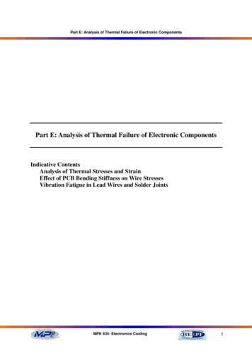
Thermal Management forElectronic Packaging03/02/2006Guoping XuSun Microsystems
CSE291: Interconnect and Packaging, UCSD, Winter 2006OutlineIntroductionHeat transfer theoryThermal resistance in electronic packagingThermal designThermal modelingThermal measurementPage 2
CSE291: Interconnect and Packaging, UCSD, Winter 2006IntroductionFunctions of Electronic PackagingPackage protectionSignal distributionPower distributionHeat dissipationPage 3
CSE291: Interconnect and Packaging, UCSD, Winter 2006IntroductionPackaging HierarchyChipPackageBoardSystemRackRoomPage 4
CSE291: Interconnect and Packaging, UCSD, Winter 2006IntroductionHigh end chip power trend600CPU Power, (W)500400UltraSparc [1]Power 4 [2]Itanium 2 [3]ITRS 2002 [4]ITRS 200530020010001990199520002005201020152020YearPage 5
CSE291: Interconnect and Packaging, UCSD, Winter 2006IntroductionCost performance chip power trend160140ITRS 2005CPU Power, (W)12010080604020020042006200820102012YearPage 62014
CSE291: Interconnect and Packaging, UCSD, Winter 2006IntroductionPower density in datacom equipmentPage 7
CSE291: Interconnect and Packaging, UCSD, Winter 2006IntroductionPower density in datacom equipmentTotal power: 24KWFootprint: 15 sq. ftPower density: 1600W/sq. ftSun Fire E25KPage 8
CSE291: Interconnect and Packaging, UCSD, Winter 2006IntroductionImpact of Device junction temperatureComputing performanceReliabilityFire hazard and/or Safety issuesPage 9
CSE291: Interconnect and Packaging, UCSD, Winter 2006Heat Transfer TheoryConductionDefinition: Conduction is a mode of heat transfer in which heat flows from aregion of higher temperaure to one of lower temperature within a medium (solid,liquid, or gases) or media in direct physical contactFourier's law: Q -KA(dT/dX)1-D conduction: Q -KA (T1-T2)/LThermal resistance: R (T1-T2)/Q L/(KA)Page 10
CSE291: Interconnect and Packaging, UCSD, Winter 2006Heat Transfer TheoryConductionContact thermal resistancePage 11
CSE291: Interconnect and Packaging, UCSD, Winter 2006Heat Transfer TheoryThermal conductivity of various packaging materialsMaterialAluminum (pure)Aluminum NitrideAluminaCopperDiamondEpoxy (No fill)Epoxy (High fill)Epoxy glassGoldLeadSiliconSilicon CarbideSilicon 2700.249.3Page 12
CSE291: Interconnect and Packaging, UCSD, Winter 2006Heat Transfer TheoryConvectionConvection: is a mode of heat transport from a solid surface to afluid and occurs due to the bulk motion of the fluid.Newton's law: Q hA (Tw- Tf)Convective thermal resistance: R 1/(hA)Effects of heat transfer coefficientConvetion mode: Natural convection, Foreced convection, phase changeFlow regime: Laminar, Turbulent flowFlow velocityy TfFluidySurface eTemperaturedistributionTwT(y)Page 13
CSE291: Interconnect and Packaging, UCSD, Winter 2006Heat Transfer TheoryTypical values of the heat transfer coefficientPage 14
CSE291: Interconnect and Packaging, UCSD, Winter 2006Heat Transfer TheoryRadiationDefinition: Radiation heat transfer occurs as a result of radiant energy emitted from abody by virtue of its temperature.Page 15
CSE291: Interconnect and Packaging, UCSD, Winter 2006Thermal Resistance-Package without heat sinkTaTbChipTtTjPackagePCBRja: Junction to air thermal resistanceRja (Tj-Ta)/PLow value is good thermal perfromanceRjc: Junction to case thermal resistanceRjc (Tj-Tc)/PΨjt: Thermal characterization parameter: Junction to package top,NOT thermal resistance.Ψjb: Thermal characterization parameter: Junction to boardPage 16
CSE291: Interconnect and Packaging, UCSD, Winter 2006Thermal Resistance-Package with heat sinkTaHeat sinkPackageDieTsTcTjRja: Junction to air thermal resistanceRja (Tj-Ta)/P Rjc Rcs RsaRjc: Junction to case thermal resistanceRjc (Tj-Tc)/PRsa: External heat sink thermal resistanceRsa (Ts-Ta)/PPage 17
CSE291: Interconnect and Packaging, UCSD, Winter 2006Thermal Resistance-PBGA package exampleTairPage 18
CSE291: Interconnect and Packaging, UCSD, Winter 2006Thermal Resistance-Impact factors for package without heat sinkDie sizePackage size, lead countPackaging material thermal condunctivityMaterial thickness in major heat flow pathNumber of viasHeat spreader or heat slugAir velocity and temperaturePC Board sizeBoard configuration and materialBoard layoutPage 19
CSE291: Interconnect and Packaging, UCSD, Winter 2006Thermal DesignConduction applicationSingle materialQDieSubstrateTcTjTc Tj - QL/(KA)tiComposite materialKin-planeLayer 1Layer 2Layer iLayer NKTthroughUniform heating on the diePage 20
CSE291: Interconnect and Packaging, UCSD, Winter 2006Thermal DesignConduction applicationHeat spreaderDieSubstrateAb As kb Ab R ba tanh H b Rsb kb Ab As 1 kb Ab R ba tanh H b 231 AbAsAb: Heat spreader base areaAs: Heat source areaHb: Heat spreader thicknessKb: Heat spreader thermal conductivityPage 21
CSE291: Interconnect and Packaging, UCSD, Winter 2006Thermal DesignConvection application-Heat sink designHfbHtfFinsHbLHeat sink baseWPage 22
CSE291: Interconnect and Packaging, UCSD, Winter 2006Thermal DesignConvection application-Heat sink designThermal resistance:Heat transfer:RbaTb Tinlet QhDhNu 7.54k airFin efficiency: o 1 At 1 f .m c p (1 e hAt o m c pLaminar flowhDhNu 0.024 Re 0.786 Pr 0.45k airAf1Turbulent flow f tanh( mH f )mH fPage 23)
CSE291: Interconnect and Packaging, UCSD, Winter 2006Thermal DesignConvection application-Heat sink designTotal static pressure loss: U ch 2L P K c 4 f app K e Dh2 Culham and Muzychka (2001)Apparent frictionfactorfappcalculationFullydeveloped flowfriction factor f f app Re 3.44 L* LDh Re 2 f Re 2 40.829 b H f 3 22.954 b H f 45 6.089 b H f f Re 24 32.527 b H f 46.721 b H fContraction losscoefficient KcExpansionlosscoefficient KeL* 0.5 2David Copeland (2000)12 1 f app Re 3.2 L* 0.57 2 2 f Re b H f 2 1f Re 4.7 19.64 b H f 1 2K c 0.42 1 K c 0.8 0.4 2K e 1 2K e 1 2 0.4 Nt fW btf b12Page 24
CSE291: Interconnect and Packaging, UCSD, Winter 2006Thermal DesignConvection application- Heat sink design ImpactfactorsAir flow rateAvailable spaceHeat sink base and fin materialFin pitch and fin thicknessHeat fluxHeat sink technologiesPage 25
CSE291: Interconnect and Packaging, UCSD, Winter 2006Thermal DesignDesign methodologyDefine requirementsAnalyze given package designIdentify major heat paths and paths for improvementsConsider and assess potential improvementsDetail analysis/modelingBuild prototypesThermal testingPage 26
CSE291: Interconnect and Packaging, UCSD, Winter 2006ModelingFinite Element Method (FEM)Software: ANSYSSolve conduction problem within package or boardRequire input data: material propoerties, package/boardconstruction/geometryBoundary conditions:Heat source distribution on the die or boardEffective convective heat transfer coefficient on the surface of the package orboardPage 27
CSE291: Interconnect and Packaging, UCSD, Winter 2006ModelingFinite Element MethodProcedure:Create package/board geometry or import from CAD fileMeshInput material properties and assign boundary conditionsSolvePost-processPage 28
CSE291: Interconnect and Packaging, UCSD, Winter 2006ModelingFinite Difference Method (FDM )Computational Fluid Dynamics (CFD)Commercial software: Flotherm, FluentSolve the temperature field and flow fieldNot only solve the conduction, also on convection, radiation andphase changeRequired input: Geometry, flow conditions, material propertiesincluding fluidMesh dependent on the chosed modelPage 29
CSE291: Interconnect and Packaging, UCSD, Winter 2006ModelingFinite Difference Method (FDM ) ExamplePage 30
CSE291: Interconnect and Packaging, UCSD, Winter 2006MeasurementPackaging thermal parametersMount package on a standard test boardMount thermocouple on top of the package centerMount thermacouple on board at the edge of packagePut package in a standard test environmentWind tunnel to vary the air speedApply known amount of powerMeasure temperature of Tj, Ta, Tb, TtCalculate Rja, Ψjt, ΨjbTaTtChipTjTbPackagePCB test boardPage 31
CSE291: Interconnect and Packaging, UCSD, Winter 2006MeasurementPackaging thermal parametersPage 32
CSE291: Interconnect and Packaging, UCSD, Winter 2006MeasurementPackaging thermal resistance RjcAll heat is removed from top of the packagePage 33
CSE291: Interconnect and Packaging, UCSD, Winter 2006MeasurementThermal interface material resistance RcsPage 34
CSE291: Interconnect and Packaging, UCSD, Winter 2006MeasurementThermal interface material resistance RcsPage 35
CSE291: Interconnect and Packaging, UCSD, Winter 2006MeasurementpettlToupirflowA tleinT2 4THeat sink thermal resistance RsawerloBlezzNoerbmhastctelowirfArsteeaRsa Ts TinletQQ k s iateemfac2TalrmerheTintsTHeat sinkT3 T2 LHeat source size: 25 mm x 25 mmPage 36
CSE291: Interconnect and Packaging, UCSD, Winter 2006MeasurementHeat sink thermal resistance RsaThe rmal Re s is tanc e , ( o C/ W )0.600Test dataPresent method (Eqs. 6-8)Teertstra [1]Copeland w rate (m /s )0.040.05Page 37
CSE291: Interconnect and Packaging, UCSD, Winter 2006Q&APage 38
Guoping XuGuoping.xu@sun.com
Power distribution Heat dissipation . CSE291: Interconnect and Packaging, UCSD, Winter 2006 Page 4 Introduction Packaging Hierarchy Chip Package Board System Rack Room . CSE291: Interconnect and Packaging, UCSD, Winter 2006 Page 5 Introduction High end chip power trend 0 100 200 300 400 500 600 1990 1995 2000 2005 2010 2015 2020 Year C PU Po w .

