Transcription
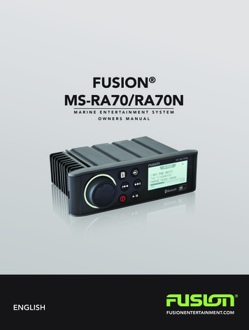
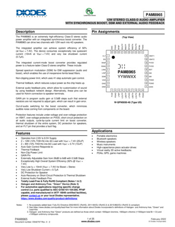
PAM896512W STEREO CLASS-D AUDIO AMPLIFIERWITH SYNCHRONOUS BOOST, SSM AND EXTERNAL AUDIO FEEDBACKPin AssignmentsThe PAM8965 is an extremely high-efficiency Class-D stereo audiopower amplifier with an integrated synchronous boost converter. ThePAM8965 can drive two channels with 12W each into 4Ω N526BSTLINP625SWSSM724SWVDD823PGNDGND922PGNDGND 1021GAINPAM8965YYWWXX13141516171819VBAT120PGNDGAIN pin to program audio gain at 0.5dB steps such that externalresistors are not required to adjust gain, which can result in gain error.12LFBNPLIM11LOUTNExternal audio feedback pins, which allow for customization of soundby using feedback network design. Alternatively, these pins can beused for Kelvin connection to speaker terminals.36LBSTNThermal foldback, which reduces output power as the chip heats up.37LPVDDNon-clipping power limit, which uses 41-step automatic gain control.38LBSTPSpread spectrum modulation (SSM) for EMI suppression (audio andboost), which enables the use of inexpensive ferrite bead filters.39LFBPThe integrated current-mode boost converter provides regulatedpower to a feature-laden Class-D stereo amplifier. These include:401PGNDThe integrated amplifier can achieve system efficiency of 92%(at VBAT 7.4V). The device consumes exceptionally low quiescentcurrent (10mA at VBAT 7.4V) and very low shutdown current(0.7μA).GND(Top View)LOUTPDescriptionW-QFN5050-40 (Type US)Out-of-audio switching for the boost converter, which minimizesaudible noise coming from components on the board.Protection features include under-voltage and over-voltage protectionon VBAT, over-voltage protection on PVDD, short circuit protection onall audio outputs, cycle-by-cycle current limit on boost converter,thermal shutdown of the entire system, DC protection for speakers,and an FLT pin that provides a fault flag.ApplicationsFeatures Operates from 2.8V to 8.5V Supply2 12W (10% THD N) into 4Ω Load with VBAT 7.4V (2SxP)2 8W (10% THD N) into 6Ω Load with VBAT 3.7V (1SxP)Auto Gain Control Responds to:Thermal FoldbackNon-Clip Power LimitGAIN PinExternally Adjustable Gain from 26dB to 6dB with 0.5dB StepsExceptionally High Overall System Efficiency (92% @ VBAT 7.4V)Very Low IQ 10mA (VBAT 7.4V) for Boost StereoVery Low Shutdown Current 0.7μADC Protection for SpeakerAuto-Recovery on Short-Circuit Protection & Thermal ShutdownExternal Audio Feedback PinsTotally Lead-Free & Fully RoHS Compliant (Notes 1 & 2)Halogen and Antimony Free. “Green” Device (Note 3)For automotive applications requiring specific changecontrol (i.e. parts qualified to AEC-Q100/101/104/200, PPAPcapable, and manufactured in IATF 16949 certified facilities),please contact us or your local Diodes uct-definitions/Notes: Portable electronicsBluetooth speakersWireless speakersMusic instrumentsHigh-capacitance piezo actuator drivesVirtual reality 3D active feedbacksPDAs, GPS, game machines1. No purposely added lead. Fully EU Directive 2002/95/EC (RoHS), 2011/65/EU (RoHS 2) & 2015/863/EU (RoHS 3) compliant.2. See https://www.diodes.com/quality/lead-free/ for more information about Diodes Incorporated’s definitions of Halogen- and Antimony-free, "Green" andLead-free.3. Halogen- and Antimony-free "Green” products are defined as those which contain 900ppm bromine, 900ppm chlorine ( 1500ppm total Br Cl) and 1000ppm antimony compounds.PAM8965Document number: DS42707 Rev. 3 - 21 of 25www.diodes.comFebruary 2022 Diodes Incorporated
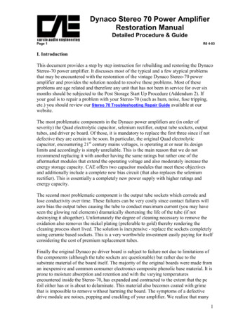
PAM8965Typical Applications Circuit 2.8V to 8.5V RFBPRBSTPROUTPENRINPRight InputLeft BAT1FLTONLOUTNLBSTNLFBNGNDPGNDPin DescriptionsPin Number123456789, 101112, 2013141516171819Pin Name GAINI22, 2324, 252627, 28293031, ��PAM8965Document number: DS42707 Rev. 3 - 2DescriptionFault flag. Open-drain output to signal system faults (VBAT UVLO or OVLO, OTP, DC input, audio SCP)Chip enable. High ON, Low OFF. Do not float this pin.Right channel audio input – PositiveRight channel audio input – NegativeLeft channel audio input – NegativeLeft channel audio input – PositiveSpread spectrum modulation. High ON, Low OFF. Do not float this pin.Internal 5V LDOAnalog signal groundNon-clip power limit setting. PLIM VDD disables power limit. Do not float this pin.Power ground for left channelLeft channel feedback – Positive. Short to LOUTP. Kelvin connect to speaker for higher performance.Left channel audio output – PositiveLeft channel boot-strap supply for high-side – PositiveLeft channel power supply for Class-D H-bridgeLeft channel boot-strap supply for high-side – NegativeLeft channel audio output – NegativeLeft channel feedback – Negative. Short to LOUTN. Kelvin connect to speaker for higher performance.Audio channel gain setting. Do not float this pin.4.5V or above 26dB (maximum gain setting).Then every 100mV is 0.5dB step, e.g., 4.4V 25.5dB, 4.3V 25dB, etc.0.5V or below 6dB (minimum gain setting)Power ground for boost converterBoost converter’s switching nodeBoost converter’s boot-strap supplyBoost converter’s output. Connect this to pin 16 and pin 35.Battery supply input for boost converter. See Application Information for decoupling requirement.Battery supply input for system. See Application Information for decoupling requirement.Power ground for right channelRight channel feedback – Negative. Short to ROUTN. Kelvin connect to speaker for higher performance.Right channel audio output – NegativeRight channel boot-strap supply for high-side – NegativeRight channel power supply for Class-D H-bridgeRight channel boot-strap supply for high-side – PositiveRight channel audio output – PositiveRight channel feedback – Positive. Short to ROUTP. Kelvin connect to speaker for higher performance.Connect to system ground2 of 25www.diodes.comFebruary 2022 Diodes Incorporated
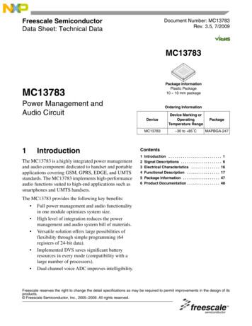
PAM8965Functional Block ConverterRFBPRBSTPDriverRF - RINNRiPWM ModulatorRiSample & HoldRINPROUTPRBSTNRFDriverROUTNRFBNPLIMAGC & FeedbackControlSSMPGNDGainDC BiasDetectionUVLO NLFBPFLTLBSTPDriverRF - LINNRiRFPWM ModulatorRiSample & HoldLINPLOUTPLBSTNDriverLOUTNLFBNAGC & FeedbackControlPGNDFigure 1. PAM8965 Block DiagramPAM8965Document number: DS42707 Rev. 3 - 23 of 25www.diodes.comFebruary 2022 Diodes Incorporated
PAM8965Absolute Maximum Ratings (@TA 25 C, unless otherwise specified.) (Note 4)SymbolParameterVBATVRINP, VRINN, VLINP, VLINNRatingUnitSupply Voltage (Pins VBAT1, VBAT2)-0.3 to 9.0VAudio Input Voltage-0.3 to 5.5VVPLIM, VGAIN, VSSMControl Input Voltage-0.3 to 6.0VVENControl Input Voltage-0.3 to VBATVMaximum Operating Junction Temperature (Note 5)-40 to 150 CTSTGStorage Temperature Range-40 to 150 CHBMHuman Body Model 2000VCDMCharged Device Model 1000VTJ MAXNote 4.Stresses greater than the Absolute Maximum Ratings specified above can cause permanent damage to the device. These are stress ratings only; functionaloperation of the device at these or any other conditions exceeding those indicated in this specification is not implied. Device reliability can be affected byexposure to absolute maximum rating conditions for extended periods of time.Recommended Operating Conditions (@TA 25 C, unless otherwise specified.)ParameterMinMaxUnitSupply Voltage (Pins VBAT1, VBAT2)2.88.5VAudio Input Voltage0.05.0VVPLIM, VGAIN, VSSMControl Input Voltage0.05.5VVENControl Input Voltage0.0VBATVMinimum Load Resistance (VBAT 5.0V)6—Minimum Load Resistance (VBAT 5.0V)4—TAOperating Free-Air Temperature Range-40 85 CTJOperating Junction Temperature Range (Note 5)-40 125 CSymbolVBATVRINP, VRINN, VLINP, VLINNRLMINNote 5.ΩThe PAM8965 incorporates an exposed thermal pad on the underside of the chip, which acts as a heatsink. The exposed pad must be connected to athermally dissipating Cu plane on the PCB for adequate power dissipation. Failure to do so may result in the device going into thermal shutdown.Thermal InformationParameterSymbolPackageRatingThermal Resistance (Junction to Ambient)θJAW-QFN5050-40 (Type US)33 C/WThermal Resistance (Junction to Case)θJCW-QFN5050-40 (Type US)10 C/WPAM8965Document number: DS42707 Rev. 3 - 24 of 25www.diodes.comUnitFebruary 2022 Diodes Incorporated
PAM8965Electrical Characteristics (VBAT 7.4V, TA 25 C, RL 4Ω 2 33μH, VPLIM VGAIN VDD, unless otherwise specified.)SymbolParameterTest ConditionMinTypMaxUnit8.5VInput Supply Voltage—2.8—VIHHigh-Level Input VoltageEN, SSM1.5——VVILLow-Level Input VoltageEN, SSM——0.5VVBAT 7.4V, RL 4Ω, PO 5W, f 1kHz—92—VBAT 3.7V, RL 6Ω, PO 3W, f 1kHz—86—VBAT 7.4V, No Load—10—VBAT 3.7V, No Load—20—VEN 0, VBAT 2.8V to 8.5V—0.75.0VBAT Rising—2.72.8VBAT FallingVBAT IQISDUVLOOVLOSystem Efficiency (Boost Stereo)Quiescent CurrentShutdown CurrentVBAT UVLO ThresholdVBAT OVLO Threshold2.302.452.55Hysteresis—0.250—VBAT Rising8.68.959.2VBAT Falling8.58.6—Hysteresis—0.350—TSDThermal Shutdown Threshold—— 150—TSD HYSThermal Shutdown Hysteresis—— 40—Thermal Foldback Trip Point—— 125—TFOLD%mAμAVV CBoost Converter (VBAT 7.4V, TA 25 C, RL 4Ω 2 33μH, VPLIM VGAIN VDD, unless otherwise specified.)SymbolVPVDDfSWParameterTest ConditionMinTypMaxUnitBoost Output Voltage——9.2—VBoost Switching Frequency——768—kHzBoost Switching Frequency in PFMNo Load5075—kHzRectifier Switch—50—mΩ—50—mΩ—8—ARONOn-State Resistance (Boost)ILIMBoost Converter Current LimitLow-Side SwitchPAM8965Document number: DS42707 Rev. 3 - 2—5 of 25www.diodes.comIL 20mAFebruary 2022 Diodes Incorporated
PAM8965Class-D Amplifier (VBAT 7.4V, TA 25 C, RL 4Ω 2 33μH, VPLIM VGAIN VDD, unless otherwise specified.)SymbolParameterContinuous Output Power, 2SxP(per Channel) (Note 6)POContinuous Output Power, 1SxP(per Channel) (Note 7)THD NTotal Harmonic Distortion NoiseIntegrated Output NoiseVNPSRRPower Supply Rejection RatioSNRSignal-to-Noise RatioTest ConditionMinTypMaxUnitVBAT 7.4V, RL 4Ω, f 1kHz, THD N 10%—12.0—WVBAT 7.4V, RL 4Ω, f 1kHz, THD N 1%—9.6—WVBAT 3.7V, RL 6Ω, f 1kHz, THD N 10%—8.0—WVBAT 3.7V, RL 6Ω, f 1kHz, THD N 1%—6.4—WVBAT 7.4V, RL 4Ω, PO 5W, CPVDD 220μF—0.035—VBAT 3.7V, RL 6Ω, PO 3W, CPVDD 220μF—0.023—Gain 20dBVIN @ AC Ground, 20Hz to 22kHzSSM OffGain 26dBVIN @ AC Ground, 20Hz to 22kHzSSM OffVIN AC Ground 100mV Supply RippleGain 26dBTHD N 1%, Gain 26dB,A-Weighted, SSM OffA-Weighting—50—No A-Weighting—70—A-Weighting—70—No A-Weighting—100—f 217Hz—-79—f 1kHz—-67—f 1kHz—100—GAIN VDD——26—GAIN GND——6—%μVrmsdBdBGVGainVOSOutput Offset VoltageVIN @ AC Ground, Gain 26dB——110mVfOSCAudio Oscillator Frequency———384—kHzGAIN VDD (26dB)——15—GAIN GND ��2.1—RINInput ResistancetONStartup Time from EN AssertedRONOn-State Resistance (Class-D)RFLTFLT Open-Drain ResistanceHigh-Side H-Bridge SwitchNotes:Low-Side H-Bridge SwitchUnder Any Fault ConditionIL 100mAdBkΩmsmΩkΩ6. For 2S x P battery configuration, minimum speaker resistance supported is 4Ω per channel.7. For 1S x P battery configuration, minimum speaker resistance supported is 6Ω per channel.PAM8965Document number: DS42707 Rev. 3 - 26 of 25www.diodes.comFebruary 2022 Diodes Incorporated
PAM8965Performance Characteristics (VBAT 7.4V, TA 25 C, RL 4Ω 33μH, VGAIN VDD, SSM On, unless otherwise specified.)1.THD N vs Power105210VBAT 7.4V, SSM ON, RL 4Ω100Hz: Magenta1kHz: Blue10kHz: RedVBAT 3.7V, SSM ON, RL 6Ω100Hz: Magenta1kHz: Blue10kHz: 0m20m50m100mW2.200m500m12510WTHD N vs Frequency10.50.21VBAT 7.4V, SSM ON, RL 4Ω1W: Blue2W: Magenta3W: Red0.50.20.10.10.050.05%VBAT 3.7V, SSM ON, RL 6Ω1W: Blue2W: Magenta3W: k20k1k2k5k10k20kHzFrequency Response4.Noise Floor 1 0-0-10-1VDD 7.4V, RL 4Ω, Gain 0-10-100-11-12-110-13-120-14-130-15Magenta: 0.1µFBlue: 1µFRed: 6020HzPAM8965Document number: DS42707 Rev. 3 - 250100200500Hz7 of 25www.diodes.comFebruary 2022 Diodes Incorporated
PAM8965Performance Characteristics (VBAT 7.4V, TA 25 C, RL 4Ω 33μH, VGAIN VDD, unless otherwise specified.) (continued)5.PSRR6.Crosstalk 0 0T TTTT TTT TT TTT T T ency vs. Output Power8.2k5k10k20kPower Limit10Efficiency (VBAT 7.4V, RL 4Ω)Efficiency (%)1kHzHz5100%290%1THDN(%)80%70%60%10TBlue: PL 2.4VRed: PL 2.2VGreen: PL 2.0VMagenta: PL 1.8V521O500m UTPU200mT0.5100m Po50m wer(20mW)10m0.20.10.0550%5m40%0.0202468Output Power (W)102m120.0110m20m50m100m200m500m11mSEInput Voltage(Vrms)9.Quiescent CurrentIQ45mAISD0.4uA40mA0.35uA0.3uA30mAISD (μA)IQ .05uA0mA3V4V5V6V7V8V9V0uA2.8VDocument number: DS42707 Rev. 3 - 23.8V4.3V4.8V5.3V5.8V6.3V6.8V7.3V7.8V8.3V8.8VVBAT (V)VBAT (V)PAM89653.3V8 of 25www.diodes.comFebruary 2022 Diodes Incorporated
PAM8965Performance Characteristics (VBAT 7.4V, TA 25 C, RL 4Ω 33μH, GAIN VDD, unless otherwise specified.)10.Start-up Waveform with EN Control11.Shutdown Waveform with EN ControlENENVDD (LDO)VDD (LDO)FLTFLTAUDIO OUTAUDIO OUTPAM8965Document number: DS42707 Rev. 3 - 29 of 25www.diodes.comFebruary 2022 Diodes Incorporated
PAM8965Detailed DescriptionThe PAM8965 is a stereo Class-D audio amplifier with integrated synchronous boost converter. The device boasts system efficiency of 92%(VBAT 7.4V), which implies that the boost converter and stereo Class-D amplifier can reach average efficiency of 96% each, negating anyadvantage of using separate ICs. The high efficiency also allows PAM8965 to deliver 2 12W (10% THD N with VBAT 7.4V) in to 2 4Ωspeakers without the need of a heat sink.The two Class-D audio channels, the integrated synchronous boost converter, and the high efficiency makes PAM8965 an extremely cost-effectivegeneral-purpose audio amplifier. The integration also results in the reduction of external components.With VBAT (input power supply) range of 2.8V to 8.5V, the PAM8965 is perfectly suited for battery applications. The wide input supply range makesit ideal for 1SxP or 2SxP Li-ion battery configurations. In addition, the PAM8965 consumes just 10mA quiescent current (V BAT 7.4V), and theshutdown current is only 0.7μA (typ), which helps to extend the battery life.The synchronous boost converter provides a regulated output of 9.2V and operates in pulse width modulation (PWM) mode for medium to highload. For light load condition, the converter transitions to pulse frequency modulation (PFM) mode to improve the efficiency of the converter. InPFM mode, to avoid the switching frequency from dropping in to the audio band, the boost converter features an out-of-audio mode, which keepsthe switching frequency above 75kHz (typ). This minimizes the possibility of audible vibrations coming from the components mounted on the PCB.In terms of performance, the integrated output noise of the audio channel at maximum gain setting of 26dB is only 70μVrms (A-weighted).Similarly, THD N is only 0.035% at PO 5W. The chopper-enabled integrator in the audio channel ensures that the output offset istypically 1mV at maximum gain.The headlining feature of PAM8965 is the provision of external audio feedback pins. While internal feedback connection takes care ofnonlinearities only in the internal feedback loop, with external feedback pins, the feedback can be Kelvin-connected to the speaker terminals. Thiseliminates parasitic resistance and inductance from bond wires, PCB trace, ferrite beads and long speaker leads from adversely affecting thefidelity of the audio signal. Furthermore, the external feedback pins allow the use of filter networks in the feedback path to customize soundwithout relying on DSP.In terms of features, the PAM8965 incorporates a 41-step (0.5dB per step) automatic gain control (AGC) system, which delivers smooth variationsin audio channel gain when responding to the following conditions: Junction temperature exceeds 125 C (thermal foldback)Output power exceeds a set threshold based on PLIM pin voltage (non-clip power limit)Volume control based on the GAIN pin voltageThe PAM8965 output can be driven in single-ended or in bridge-tied-load (BTL) configuration.Spread spectrum modulation (SSM) allows the use of inexpensive ferrite bead filters and yet meet EMI specification. Although boost switchingfrequency (768kHz) is twice that of Class-D PWM frequency (384kHz), nevertheless, the spread added on both systems due to SSM issynchronized. This ensures audible beats are not generated due to difference in switching frequencies.The start-up time, defined as the time between EN asserted and audible output from the speakers, is only 15ms. This includes the boost converterstart-up and audio channel wake-up along with the pre-charge of the DC-blocking capacitors at audio Inputs. The advantage of this fast start isthat the device does not require mute control. The device can be enabled when audio output is required, and disabled when audio output is off,consuming only 0.7μA in the off state.The PAM8965 has a multitude of protection features, which include under-voltage and over-voltage lock out on VBAT, over-voltage lock out onPVDD, short circuit protection on all audio outputs, cycle-by-cycle current limit on the boost converter, thermal shutdown of the entire system,speaker protection against DC audio, and an FLT pin that provides a fault flag.PAM8965Document number: DS42707 Rev. 3 - 210 of 25www.diodes.comFebruary 2022 Diodes Incorporated
PAM8965Application InformationAudio InputThe PAM8965 supports differential and single-ended input configurations.Differential InputDifferential input operation minimizes noise that appears common on both the input lines of the channel. To apply a differential input, connect thepositive terminal of the audio source to xINP pin and connect the negative terminal to xINN pin, where x can be L or R for Left and Right channels,respectively.It is best to AC-couple the audio source to xINP and xINN pins.Single-Ended InputTo apply a single-ended input, connect the audio source to xINN pin. AC-ground xINP pin by connecting a capacitor equal in value to the DCblocking capacitor on xINN pin. xINP input should be AC-grounded at the audio source, rather than at the device input, for achieving the bestnoise performance.AC- or DC-Coupled Audio SignalThe preferred method to provide audio input is to AC-couple the audio source to xINP and xINN pins with capacitors.It is also possible to DC-couple the audio source, provided the common-mode voltage of the audio source is close to 2.5V. If output impedance ofaudio source is high, or the common-mode voltage is far away from 2.5V, then risk of pop noise at turn-on is higher for a DC-coupled audio signal.In addition, the further the common-mode voltage of the audio source is away from 2.5V, the more the audio source will have to source/sink DCcurrent.Input Capacitor SelectionFor best THD performance, film capacitors are recommended at the Audio Inputs because they offer excellent stability over a wide temperatureand voltage range. Use ceramic capacitors for cost-sensitive applications.Input resistance of the PAM8965 can vary from 15kΩ at 26dB to 105kΩ at 6dB Gain setting. As a result, for AC-coupled applications, the cut-offfrequency of high-pass filter that is formed at the input, varies with the Gain setting. The -3dB cut-off frequency is given by (1). Using the minimumvalue of RIN, which is 15kΩ, provides a minimum recommended value of CIN 1μF to pass 20Hz to the amplifier.fC 12πR IN CIN(1)RF-3dBCINAudio InputRINfC(a)(b)Figure 2. (a) Audio Input Interface, (b) -3dB Cut-Off Frequency of Audio Input High-Pass FilterPAM8965Document number: DS42707 Rev. 3 - 211 of 25www.diodes.comFebruary 2022 Diodes Incorporated
PAM8965Application Information (continued)Audio Channel GainThe PAM8965 audio channel gain is defined using the GAIN pin. The channel gain can be set between 26dB and 6dB at 0.5dB steps. Channelgain is accurate when it is based on internal resistors only. If using external resistor on the inputs to set the gain, then the device-to-device gainvariation will be large. More importantly, even right and left channel gain will not match because the use of external resistors makes the channelgain dependent on the absolute values of these resistors.Connect a resistor divider between VDD and GND pins to define a voltage on the GAIN pin (Figure 3). This is important because GAIN isreferenced to these supplies. Table 1 provides the resistor ratio required on the GAIN pin to obtain the required channel gain. Figure 4 show therelationship between the GAIN pin voltage and audio channel gain assuming VDD 5.0V. Aim for R1 R2 100kΩ to reduce current wasted in thedivider. Place R1 and R2 close to the GAIN pin. A small 1nF capacitor can be placed near the pin to filter noise.GAIN Resistor Ratio R2R1 R 2(2)VDD (Pin 8)21R1GAINC1R2Figure 3. GAIN Resistor Divider SetupRatioGain (dB)RatioGain (dB)RatioGain (dB)RatioGain (dB)RatioGain (dB)RatioGain (dB)GND to 16.00.6419.50.7823.00.90 to 1.026.0Table 1. GAIN Resistor Ratio vs. Audio Channel Gain (dB)Channel Gain AIN Pin (V)Figure 4. Channel Gain vs. GAIN Pin Voltage (with VDD 5.0V)PAM8965Document number: DS42707 Rev. 3 - 212 of 25www.diodes.comFebruary 2022 Diodes Incorporated
PAM8965Application Information (continued)Enable-Disable ControlEN pin on the PAM8965 is active-high. Voltage above VIH (1.5V) enables the device. EN pin is not limited to 5V operation and can be connecteddirectly to VBAT, which has a maximum specification of 8.5V.When EN pin is pulled below VIL (0.5V), this disables the device and the audio outputs are muted and the boost converter is turned off. In thedisabled or shutdown state, the device consumes only 0.7μA (typ). To achieve the best pop-noise performance, it is recommended to first disablethe device before removing the power supply. Figure 5 shows one possible power-up and power-down sequence that would minimise output popnoise.After device turn-off, minimum wait of 400ms is required before asserting EN again.EN pin has to be driven and cannot be left floating.Power onPower offVBATENFigure 5. Optional Power-up & Power-down SequenceNon-Clip Power Limit (PLIM)The PAM8965 features a non-clipping power limit that protects the speakers from burn out. PLIM pin should be set such that the maximum powerrating of the speaker is matched with the maximum output power of the PAM8965.PLIM Resistor Ratio R2R1 R 2(3)VDD (Pin 8)R111PLIMR2Figure 6. PLIM Resistor Divider SetupConnect a resistor divider between VDD and GND pins to define a voltage on PLIM pin as shown in Figure 6. This is important because the PLIMfunction is referenced to these supplies. Aim for R1 R2 20kΩ. Place R1 and R2 close to the PLIM pin. Table 2 shows resistor ratio required onthe PLIM pin to set the required output power.Maximum PLIM voltage is 2.4V when using Power Limit function. PLIM 2.4V will result in POUT 9W for VBAT 7.4V and RL 4Ω. To disablethe power limit function, connect PLIM to VDD (Pin 8).PAM8965Document number: DS42707 Rev. 3 - 213 of 25www.diodes.comFebruary 2022 Diodes Incorporated
PAM8965Application Information (continued)RL 4Ω, VBAT 7.4VRL 6Ω, VBAT 3.7VR1 (Ω)R2 (Ω)RatioVPLIM (V)POUT (W)POUT 409.006.00———VDD11.508.00—Table 2. PLIM Pin Voltage (for VDD 5.0V) or Resistor Ratio for Output Power (per Channel)If instantaneous output power exceeds the defined PLIM value, then the amplifier triggers an attack cycle. Effectively, this begins a process of thePAM8965’s amplifier gain stepping down with 0.5dB steps for every attack cycle. The gain is reduced with successive attack cycles until the outputpower drops to the value defined by the PLIM pin voltage as shown in Figure 7.9.0RL 4 OhmRL 6 OhmOutput Power (W)8.07.06.05.04.03.02.01.00.01.01.52.02.5PLIM Pin (V)Figure 7. Output Power (per Channel) vs. PLIM Pin Voltage (for VDD 5.0V)Adjusting the amplifier’s closed-loop gain to control the output power results in an extremely smooth control, which prevents harsh sounds due tosaturation. This type of control avoids the output signal from being clipped, thus providing a much nicer listening experience. Figure 8 illustratesthe non-clip power limit attack cycle.Attack time for power limit is 50μs, and release time is elFigure 8. Non-Clip Power Limit Attack CyclePAM8965Document number: DS42707 Rev. 3 - 214 of 25www.diodes.comFebruary 2022 Diodes Incorporated
PAM8965Application Information (continued)Thermal FoldbackDevice protection due to OTP results in abrupt turn-off and turn-on of sound. The primary purpose of thermal foldback (ThmFB) is to avoidinterruption of sound due to OTP. The PAM8965’s ThmFB feature works by stepping down the closed-loop gain of the amplifier once the dietemperature reaches the ThmFB threshold. As the gain is stepped down, output power is reduced, which results in lower power dissipationthereby reducing the possibility of the device shutting down due to OTP.Thermal Foldback threshold is set at 125 C. As with PLIM, this feature controls the closed-loop gain of the amplifier resulting in smoothtransitions in the audio output. The full AGC range of 26dB to 6dB is available for ThmFB feature. Figure 9 shows an illustration of ThmFB attackand release cycles. The attack time is set at 170ms and the release time is meGainOutputSignalFigure 9. Thermal Foldback Attack/Release CycleFault Flag (FLT)The PAM8965 features a fault flag, which is an open-drain output on the FLT pin. This pin supports full voltage range up to VBAT.The following abnormal conditions are flagged on the FLT pin:UVLO on VBAT OVLO on VBAT Over-temperature shutdown (OTP) DC detected on any of the audio inputs (no auto-recovery on this fault) Short circuit protect (SCP) on any audio output The open-drain FET turns on when fault occurs, and turns off once the fault is cleared. It is recommended to connect a 100kΩ pull-up resistor fromFLT pin to any voltage up to VBAT. If the aim is to minimize PCB component count, then FLT pin can be left floating.Under Voltage Lock Out (UVLO) on VBATWhen VBAT drops below the UVLO threshold of 2.45V (typ), the device enters a quasi-disabled state where the boost converter and the audiochannels are turned off but a few blocks remain powered up. As a result, the current drawn from the battery in this state is higher than I SD. Thedevice will auto-recover and repeat the start-up sequence once VBAT goes above 2.8V.Over Voltage Lock Out (OVLO) on VBATWhen VBAT goes above the OVLO threshold of 8.9V (typ), the device enters a quasi-disabled state similar to UVLO condition. The device will autorecover and repeat the start-up sequence once VBAT drops 350mV below the OVLO threshold.PAM8965Document number: DS42707 Rev. 3 - 215 of 25www.diodes.comFebruary 2022 Diodes Incorporated
PAM8965Application Information (continued)Over-Temperature ProtectionTo prevent device from over-temperature stress, the PAM8965 incorporates thermal shutdown, which turns the device off when junctiontemperature exceeds 150 C (typ). OTP has a hysteresis of 40 C. The system will resume operation after junction temperature goes below 110 C (typ). In OTP state, both the audio channels and the boost converter are turned off. This is not a latched fault.For 1SxP applications, the high boost ratio results in very high boost switch currents. This reduces the efficiency of the system thereby increasingthe junction temperature of the device. Depending on the physical enclosure the device is placed in, it may be necessary to use a heatsink ifoutputting maximum power with maximum boost ratio.DC Audio DetectionThe PAM8965 analyses the PWM output waveform to detect if a DC signal is being applied to the speakers. This can occur due to damagedcapacitors at the audio inputs or due to shorts on the PCB. A DC signal can quickly over-heat and damage the speakers. By detecting DC in theoutput waveform rather than at the input, DC protection will kick-in at the same output level irrespective of the GAIN setting.Once DC is detected on any of the outputs (P or N of right or left channel), both audio channels are turned off with all four audio outputs changingstate to Hi-Z. The audio channels will remain off because this fault condition is latched. This ensures the speaker is protected against repeatedexposure to DC voltage/current, which can cause damage.Cycling EN or VBAT will clear the fault.Short-Circuit Protection with Auto-Recovery for Audio OutputsIf the PAM8965 detect
WITH SYNCHRONOUS BOOST, SSM AND EXTERNAL AUDIO FEEDBACK Description The PAM8965 is an extremely high-efficiency Class-D stereo audio power amplifier with an integrated synchronous boost converter. The PAM8965 can drive two channels with 12W each into 4Ω speakers. The integrated amplifier can achieve system efficiency of 92% (at V BAT 7.4V).