Transcription
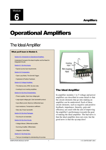
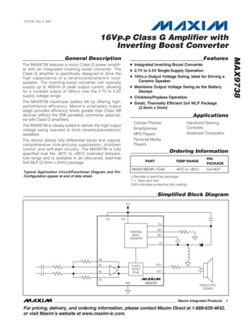
19-3700; Rev 0; 3/0816VP-P Class G Amplifier withInverting Boost ConverterFeatures Integrated Inverting Boost Converter 2.7V to 5.5V Single-Supply Operation 16VP-P Output Voltage Swing, Ideal for Driving aCeramic SpeakerThe MAX9738 features a mono Class G power amplifier with an integrated inverting boost converter. TheClass G amplifier is specifically designed to drive thehigh capacitance of a ceramic/piezoelectric loudspeaker. The inverting boost converter can typicallysupply up to 400mA of peak output current, allowingfor a constant output of 16VP-P over the 2.7V to 5.5Vsupply voltage range. Maintains Output Voltage Swing as the BatteryDecays Clickless/Popless Operation Small, Thermally Efficient 5x4 WLP Package(2.5mm x 2mm)The MAX9738 maximizes battery life by offering highperformance efficiency. Maxim’s proprietary outputstage provides efficiency levels greater than Class ABdevices without the EMI penalties commonly associated with Class D amplifiers.ApplicationsCellular PhonesSmartphonesMP3 PlayersPersonal MediaPlayersThe MAX9738 is ideally suited to deliver the high outputvoltage swing required to drive ceramic/piezoelectricspeakers.The device utilizes fully differential inputs and outputs,comprehensive click-and-pop suppression, shutdowncontrol, and soft-start circuitry. The MAX9738 is fullyspecified over the -40 C to 85 C extended temperature range and is available in an ultra-small, lead-free5x4 WLP (2.5mm x 2mm) package.Handheld GamingConsolesNotebook ComputersOrdering InformationPARTMAX9738EWP TG45Typical Application Circuit/Functional Diagram and PinConfiguration appear at end of data sheet.TEMP RANGEPINPACKAGE-40 C to 85 C5x4 WLP Denotes a lead-free package.T Tape and reel.G45 indicates protective die coating.Simplified Block LXFB IN IN-CLASS GOUTPUTSTAGE -OUT OUT-FBGNDMAX9738PIEZOELECTRICSPEAKERMaxim Integrated ProductsFor pricing, delivery, and ordering information, please contact Maxim Direct at 1-888-629-4642,or visit Maxim’s website at www.maxim-ic.com.1MAX9738General Description
MAX973816VP-P Class G Amplifier withInverting Boost ConverterABSOLUTE MAXIMUM RATINGS(Voltages with respect to GND.)VDD, VBAT . -0.3V to 6VVDD to VBAT . -0.1V to 0.1VVSS .Capacitor Connection Only,(VBAT - 10V) to 0.3VOUT , OUT- .-6V to (VDD 0.3V)(OUT to OUT-) . -8.7V to 8.7VIN , IN-, FB , FB-, ISET .-0.3V to (VDD 0.3V)LX .(VDD - 11.5V) to (VDD 0.3V)BST.(LX - 0.3V) to (LX 6V)SHDN.-0.3V to 6VContinuous Current into/out ofOUT , OUT-, VBAT, VSS, VDD .400mAAny Other Pin .20mADuration of OUT , OUT- Short Circuit toVDD, GND, VSS (VSS -6V).ContinuousRMS Current per BumpVBAT, LX .800mAContinuous Power Dissipation (TA 70 C)20-Bump UCSP (derate 10mW/ C above 70 C) .800mWOperating Temperature Range . -40 C to 85 CJunction Temperature . 150 CStorage Temperature Range . -65 C to 150 CBump Temperature (soldering) Reflow. 235 CStresses beyond those listed under “Absolute Maximum Ratings” may cause permanent damage to the device. These are stress ratings only, and functionaloperation of the device at these or any other conditions beyond those indicated in the operational sections of the specifications is not implied. Exposure toabsolute maximum rating conditions for extended periods may affect device reliability.ELECTRICAL CHARACTERISTICS(VDD VBAT SHDN 3.6V, GND 0V, VDD - VSS 9V, RISET 100kΩ, RIN RIN- 10kΩ, RFB RFB- 10kΩ, CL open, RL ,C1 10μF, C2 10μF, C3 0.1μF, C4 0.1μF, TA TMIN to TMAX, unless otherwise noted. Typical values are at TA 25 C.) (Note mAGENERALSupply Voltage RangeTotal Quiescent CurrentVDDIDD TOTMaximum Total QuiescentCurrentIDD TOT MAXShutdown Supply CurrentISHDNTurn-On TimeISET Bias VoltagetONVISETInferred from PSRR test2.7IVDD IVBAT (boost converter disabled)Typical application circuit (Note 2)16.5SHDN GND0.6Time from shutdown or power-on to fulloperation (CIN 0.1μF)100.91.0mA2μAms1.1VThermal Shutdown Threshold150 CThermal Shutdown Hysteresis15 C2
16VP-P Class G Amplifier withInverting Boost Converter(VDD VBAT SHDN 3.6V, GND 0V, VDD - VSS 9V, RISET 100kΩ, RIN RIN- 10kΩ, RFB RFB- 10kΩ, CL open, RL ,C1 10μF, C2 10μF, C3 0.1μF, C4 0.1μF, TA TMIN to TMAX, unless otherwise noted. Typical values are at TA 25 C.) (Note 1)PARAMETERSYMBOLCONDITIONSMINTYPMAX 3.7 15UNITSSPEAKER AMPLIFIEROutput Offset VoltageVOSInput DC Bias VoltageVBIASCommon-Mode Output LevelVCMClick-and-Pop LevelKCPVoltage GainAVContinuous Output PowerOutput VoltagePOUTVOUTCommon-Mode RejectionRatioCMRRVDD 2.7V or 5.5VTA 25 CTMIN TA TMAX(Note 3)1.01.231.5VDD 2.7V0.751.171.60VDD 5.5V2.4033.45Peak voltage into/out of shutdown,A-weighted, 32 samples per second(Note 4)VDD 2.7V (Note 5)Total Harmonic Distortion PlusNoisePSRRTHD N-6011.5VBAT VDD 2.7V or 5.5V, RLOAD 8Ω,THD N 1%THD N 1%, CIN 0.1μF, CL 1.6μF,RL 20Ω, TA 25 C(Note 6)5.5VBAT VDD 2.7V, f 10kHz5.0Dynamic RangeSNRDRSHDN Input ThresholdSHDN Input Leakage CurrentVIHVV12.5dBWVRMSVBAT VDD 3.6V, f 1kHz5.656.3VBAT VDD 3.6V, f 10kHz5.376.0fIN 1kHz (Note 7)6054dB60f 217Hz, 100mVP-P ripple80f 1kHz, 100mVP-P ripple70f 20kHz, 100mVP-P ripple60f 1kHz, VOUT 16VP-P, CL 1.6μF,RL 20Ω0.2f 10kHz, VOUT 15.2VP-P, CL 1.6μF,RL 20Ω0.4dB0.5%VOUT 5VRMS, A-weighted (Note 6)A-weighted (Note 8)355mA95dB110dB1.40.4VILIIH, IILmVdBV0.25Peak Load CurrentSignal-to-Noise Ratio12VBAT VDD 2.7V, f 1kHzVDD 2.7V to 5.5VPower-Supply Rejection Ratio 30-3 3VμA3MAX9738ELECTRICAL CHARACTERISTICS (continued)
MAX973816VP-P Class G Amplifier withInverting Boost ConverterELECTRICAL CHARACTERISTICS (continued)(VDD VBAT SHDN 3.6V, GND 0V, VDD - VSS 9V, RISET 100kΩ, RIN RIN- 10kΩ, RFB RFB- 10kΩ, CL open, RL ,C1 10μF, C2 10μF, C3 0.1μF, C4 0.1μF, TA TMIN to TMAX, unless otherwise noted. Typical values are at TA 25 C.) (Note ERTING BOOST CONVERTER (VDD - VSS -8.75V)Switching FrequencyFET On-TimetFONMinimum FET Off-TimePeak Output CurrentVDD 3V, typical application circuit(Note 9)FET Current Limit (DC)TA 25 C (Note 10)FET Current Limit (Transient)Typical application circuit, inductor ISATrating 1.7AFET mA1.351.6ILX 100mA, TA 25 C8.15AA0.20.26Ω8.99.60VRegulated Output VoltageVBAT - VSSTransient Load Regulation0 to 400mA load step, typical applicationcircuit300mVMaximum Output RippleILOAD 20mA, typical application circuit200mVP-PBST Shutdown LeakageSHDN 0V, LX 0V, BST 5V0.011μAVBAT Shutdown CurrentVBAT VDD, SHDN 0V, LX 0V,BST 5V0.013μALX Shutdown LeakageLX 0V, SHDN 0V, BST 5V0.013μAAll devices are 100% production tested at TA 25 C. Specifications over temperature limits are guaranteed by design.Total quiescent current depends on overall efficiency and varies with the LX inductor value and ESR, diode turn-on voltage, and the parasitic losses in all external components.Note 3: Input DC bias voltage determines the maximum voltage swing of the input signal. An input signal with an amplitudegreater than the input DC bias voltage results in clipping.Note 4: Amplifier inputs AC-coupled to GND.Note 5: Voltage gain is defined as [VOUT - VOUT-]/[VIN - VIN-].Note 6: VOUT is defined as [VOUT - VOUT-].Note 7: Matching of external AC-coupling input capacitors and gain resistors is critical to achieving good CMRR.Note 8: Dynamic range calculated by measuring the RMS voltage difference between a -60dBFS output signal and the noise floor,then adding 60dB. Full scale is defined as the output signal needed to achieve 1% THD N.Note 9: Peak output current depends on external power-supply components and the signal frequency.Note 10: Boost converter current limit is tested with a DC sweep. Actual current-limit values under transient conditions may be higher. At high input supply, VBAT, and low inductance, L, transient current limit might be higher than 1.7A.Note 1:Note 2:4
16VP-P Class G Amplifier withInverting Boost ConverterVDD 2.7VVDD 3.6V1THD N (%)0.10.10.01VOUT 5.5VRMS0.010.01VOUT 1.2VRMSVOUT 2VRMS0.001VOUT 0k100kFREQUENCY (Hz)FREQUENCY (Hz)TOTAL HARMONIC DISTORTION PLUSNOISE vs. OUTPUT VOLTAGETOTAL HARMONIC DISTORTION PLUSNOISE vs. OUTPUT VOLTAGETOTAL HARMONIC DISTORTION PLUSNOISE vs. OUTPUT VOLTAGEfIN 5kHz1fIN 10kHz0.1fIN 1kHzVDD 4.2V0.10.001fIN 1kHz0.0010.00134567012345OUTPUT VOLTAGE (VRMS)OUTPUT VOLTAGE (VRMS)TOTAL QUIESCENT CURRENTvs. SUPPLY VOLTAGESHUTDOWN CURRENTvs. SUPPLY VOLTAGE119IQ IVDD IVBAT54SUPPLY VOLTAGE (V)56234567POWER-SUPPLY REJECTION RATIOMAX9738 toc080.8VRIPPLE PSRR (dB)1307OUTPUT VOLTAGE (VRMS)0.9SHUTDOWN CURRENT (μA)1561.0MAX9738 toc071730.10.010.012fIN 10kHzfIN 1kHz0.011fIN 5kHz1fIN 10kHzTHD N (%)THD N (%)1MAX9738 toc06VDD 3.6VMAX9738 toc09fIN 5kHz10MAX9738 toc0510MAX9738 toc04VDD 2.7V2100FREQUENCY (Hz)1000.1VOUT 5.5VRMSVOUT 3.5VRMSTHD N (%)VDD 4.2V1THD N (%)THD N (%)110MAX9738 toc0210MAX9738 toc0110TOTAL QUIESCENT CURRENT (mA)TOTAL HARMONIC DISTORTION PLUSNOISE vs. FREQUENCYTOTAL HARMONIC DISTORTION PLUSNOISE vs. FREQUENCYMAX9738 toc03TOTAL HARMONIC DISTORTION PLUSNOISE vs. FREQUENCY0.1-800-902.02.53.03.54.04.5SUPPLY VOLTAGE (V)5.05.56.0101001k10k100kFREQUENCY (Hz)5MAX9738Typical Operating Characteristics(VDD VBAT SHDN 3.6V, GND 0V, RISET 100kΩ, RIN RIN- 10kΩ, RFB RFB- 10kΩ, CL 1.6μF, RL 20Ω, C1 10μF,C2 10μF, C3 0.1μF, C4 0.1μF, TA 25 C, Typical Application Circuit.)
Typical Operating Characteristics (continued)(VDD VBAT SHDN 3.6V, GND 0V, RISET 100kΩ, RIN RIN- 10kΩ, RFB RFB- 10kΩ, CL 1.6μF, RL 20Ω, C1 10μF,C2 10μF, C3 0.1μF, C4 0.1μF, TA 25 C, Typical Application Circuit.)POWER DISSIPATION DD 2.7V, fIN 1kHz1234900700600500400300100VDD 3.6V, fIN 1kHzVDD 4.2V, fIN 1kHz005PACKAGE DISSIPATION LIMIT800200000PACKAGE DISSIPATION LIMIT800POWER DISSIPATION (mW)PACKAGE DISSIPATION LIMIT1000MAX9738 toc1190012345OUTPUT VOLTAGE (VRMS)OUTPUT VOLTAGE (VRMS)MAXIMUM OUTPUT VOLTAGEvs. VBAT SUPPLYSTARTUP WAVEFORM061234MAX9738 toc136.46SHUTDOWN WAVEFORMMAX9738 toc15MAX9738 toc146.65OUTPUT VOLTAGE (VRMS)SHDN5V/divSHDN5V/divOUT - OUT500mV/divOUT - OUT500mV/div6.26.05.85.61% THD N5.42.53.03.54.04.55.05.510ms/div10ms/divVSS RIPPLE WITH 1kHz OUTPUT WAVEFORMEFFICIENCYvs. VSS LOAD CURRENTVBAT SUPPLY (V)MAX9738 toc17MAX9738 toc1690MAX9738 toc18CLASS G OUTPUT WAVEFORM80OUT 5V/divVSS500mV/divOUT5V/divOUT - OUT10V/divOUT - OUT10V/div70EFFICIENCY (%)POWER DISSIPATION (mW)1000MAX9738 toc101000800POWER DISSIPATIONvs. OUTPUT VOLTAGEPOWER DISSIPATIONvs. OUTPUT VOLTAGEMAX9738 toc12POWER DISSIPATIONvs. OUTPUT VOLTAGEOUTPUT VOLTAGE (VRMS)MAX973816VP-P Class G Amplifier withInverting Boost Converter60504030VDD 3.6VDC LOAD ON VSS ONLYINPUT AC-GROUNDEDNO LOAD ON AMPLIFIER201% THD N1% THD N100200μs/div200μs/div050100 150 200 250 300 350 400VSS LOAD CURRENT (mA)6
16VP-P Class G Amplifier withInverting Boost ConverterBOOST CONVERTER-INDUCTORCURRENT SCOPE PHOTO (3.6V)BOOST CONVERTER-INDUCTORCURRENT SCOPE PHOTO (3.6V)MAX9738 toc19MAX9738 toc20fIN 10kHzfIN divILOAD500mV/divILOAD500mV/divOUT - OUT10V/divOUT - OUT10V/div20μs/div4μs/divBOOST CONVERTER-INDUCTORCURRENT SCOPE PHOTO (4.2V)BOOST CONVERTER-INDUCTORCURRENT SCOPE PHOTO (4.2V)MAX9738 toc22MAX9738 toc21fIN 10kHzfIN divILOAD500mV/divILOAD500mV/divOUT - OUT10V/divOUT - OUT10V/div4μs/div20μs/divOUTPUT AMPLITUDEvs. FREQUENCYVOUT 2VRMS18166145VDD 3.6VVDD 2.7V4GAIN (dB)OUTPUT AMPLITUDE (VRMS)MAX9738 toc23VDD 4.2V720MAX9738 toc24FREQUENCY RESPONSE812108362411% THD N200101001kFREQUENCY (Hz)10k100k101001k10k100kFREQUENCY (Hz)7MAX9738Typical Operating Characteristics (continued)(VDD VBAT SHDN 3.6V, GND 0V, RISET 100kΩ, RIN RIN- 10kΩ, RFB RFB- 10kΩ, CL 1.6μF, RL 20Ω, C1 10μF,C2 10μF, C3 0.1μF, C4 0.1μF, TA 25 C, Typical Application Circuit.)
16VP-P Class G Amplifier withInverting Boost ConverterMAX9738Pin DescriptionPINNAMEA1, A2VBATFUNCTIONA3SHDNA4FB-Negative Polarity Amplifier FeedbackA5IN-Negative Polarity Amplifier InputB1, B2LXInverting-Boost Inductor Connection. Connect a 1.5μH to 2.2μH inductor between LX and GND.B4FB Positive Polarity Amplifier FeedbackB5IN Positive Polarity Amplifier InputC1BSTBoost Flying Capacitor Connection. Connect a 0.1μF capacitor between BST and LX.C2, C4VSSClass G Amplifier Negative Power-Supply Input. Connect to inverting boost converter outputnode. Bypass VBAT with a 10μF ceramic capacitor.Battery Connection. Bypass to GND with a 10μF ceramic capacitor.Active-Low Shutdown. Connect to VDD for normal operation.C5ISETBoost Current Set. Connect a 100kΩ resistor from ISET to GND.D1, D5VDDPower-Supply Input. Connect to VBAT.D2OUT-Negative Polarity Amplifier OutputD3GNDGroundD4OUT Positive Polarity Amplifier OutputDetailed DescriptionThe MAX9738 Class G power amplifier with invertingboost converter is the latest in linear amplifier technology. The Class G output stage offers improved performance over a Class AB amplifier while increasingefficiency to extend battery life. The integrated invertingboost converter generates a negative supply capableof delivering up to 400mA. The negative supply is onlyused when the output signal requires a larger supplyvoltage differential. As the battery voltage drops, theboost converter output becomes more negative tomaintain amplifier output swing all the way down toVBAT 2.7V.The Class G output stage and the inverting boost converter allow the MAX9738 to deliver a 16VP-P voltageswing, up to four times greater than a Class AB amplifier.Class G OperationThe MAX9738 Class G amplifier is a linear amplifier thatoperates within a low (VDD to GND) and high (VDD toVSS) supply range. Figure 1 illustrates the transitionfrom the low to high supply range. For small signals,the device operates within the lower (VDD to GND) supply range. In this range, the operation of the device isidentical to a traditional single-supply Class AB amplifier where:ILOAD IN18As the output signal increases so a wider supply isneeded, the device begins its transition to the highersupply range (VDD to VSS) for the large signals. Toensure a seamless transition between the low and highsupply ranges, both of the lower transistors are on sothat:ILOAD IN1 IN2As the output signal continues to increase, the transition to the high supply is complete. The device thenoperates from the higher supply range, where the operation of the device is identical to a traditional dual-supply Class AB amplifier where:ILOAD IN2During operation, the output common-mode voltage ofthe MAX9738 adjusts dynamically as the device transitions between supply ranges.Utilizing a Class G output stage with an inverting boostconverter allows the MAX9738 to realize a 17.5VP-Poutput swing with a 5V supply. A traditional Class ABamplifier would need to be powered with a 5V supplyto generate the same output swing at half the efficiencyof the Class G.
16VP-P Class G Amplifier withInverting Boost ConverterMAX9738BTL CLASS G SUPPLY N1IN2N1ONN2ONPZLIN2N1OFFN2ONVSSVSSVSSLOW SUPPLY RANGE OPERATIONIP IN1SUPPLY TRANSITIONIP IN1 IN2HIGH SUPPLY RANGE OPERATIONIP IN2Figure 1. Class G Supply TransitionInverting Boost ConverterThe MAX9738 features an integrated inverting boostconverter with an on-chip n-channel MOSFET to provide an inverted supply rail that can supply up to400mA over the 2.7V to 5.5V positive supply range.The boost converter generates the negative supply rail(VSS) needed to create the higher supply range thatallows the output of the device to operate over agreater dynamic range as the battery supply collapsesover time. The converter uses a constant on-time,pulse-frequency modulation (PFM) architecture. Theintegrated MOSFET and the built-in soft-start functionreduce the number of external components requiredwhile controlling inrush currents. The inverting boostregulator achieves soft-start by decreasing both peakinductor current limit and the constant on-time until VSSvoltage reaches 90% of its regulation level.PFM Controller BlockAn error amplifier compares the output voltage to aninternal target voltage. Once the output voltage issmaller than the regulation level, the controller sets aflip-flop, turning on the n-channel MOSFET and applying the battery voltage across the inductor. The currentthrough the inductor ramps up linearly, storing energyin its magnetic field. Once the on-time timer expires, orthe inductor current reaches the current limit, the controller resets the flip-flop and turns off the MOSFET.Since the inductor current is continuous, a transversepotential develops across the inductor that turns on thediode (D1). This discharge condition forces the currentthrough the inductor to ramp back down, transferringthe energy stored in the magnetic field to the outputcapacitor and the load. The MOSFET remains off untilthe minimum off-time is expired or the output voltage isabove the regulation level.9
MAX973816VP-P Class G Amplifier withInverting Boost ConverterShutdown ModeThe MAX9738 has a shutdown mode that reduces powerconsumption and extends battery life. Driving SHDN lowplaces the MAX9738 in a low-power (0.6μA) shutdownmode. Connect SHDN to VDD for normal operation.MAX9738FB Click-and-Pop SuppressionThe MAX9738 Class G amplifier features Maxim’s comprehensive, industry-leading click-and-pop suppression. During startup, the click-and-pop suppressioncircuitry eliminates any audible transient sources internal to the device.CIN Applications InformationCIN-Differential Input AmplifierThe MAX9738 features a differential input configuration,making the device compatible with many CODECs, andoffering improved noise immunity over a single-endedinput amplifier. In devices such as PCs, noisy digitalsignals can be picked up by the amplifier’s inputtraces. The signals appear at the amplifiers’ inputs ascommon-mode noise. A differential input amplifieramplifies the difference of the two inputs, and signalscommon to both inputs are canceled out. When configured for differential inputs, the voltage gain of theMAX9738 is set by:A V 20log[4 (RFBRIN)] (dB)where AV is the desired voltage gain in dB. RIN shouldbe equal to RIN-, and RFB should be equal to RFB-.The Class G output stage has a fixed gain of 4V/V(12dB). Any gain or attenuation set by the externalinput stage resistors add to or subtract from this fixedgain. See Figure 2.In differential input configurations, the common-moderejection ratio (CMRR) is primarily limited by the external resistor and capacitor matching. Ideally, to achievethe highest possible CMRR the following external components should be selected where:RFB RFB RIN RINand10CIN CIN-RFB RIN IN IN- -CLASS GOUTPUTSTAGERINRFB-FB-Figure 2. Gain SettingDriving a Ceramic SpeakerApplications that require a thin profile, such as today’smobile phones, demand that components have a smallform factor. Dynamic loudspeakers that use a cone andvoice coil typically cannot conform to the heightrequirements. The option for these applications is touse a ceramic/piezoelectric loudspeaker.Ceramic speakers are much more capacitive than aconventional loudspeaker. Typical capacitance valuesfor such a speaker can be greater than 1μF. High peakto-peak voltage drive is required to achieve acceptablesound pressure levels. The high output voltage requirement coupled with the capacitive nature of the speakerdemand that the amplifier supply much more current athigh frequencies than at lower frequencies. Above 5kHzthe typical speaker impedance can be less than 20Ω.The MAX9738 is ideal for driving a capacitive ceramicspeaker. The high boost converter current limit allowsfor a flat frequency response out to 20kHz while maintaining high output voltage swings. Figure 3 shows atypical circuit for driving a ceramic speaker.A 20Ω series resistance is required between the amplifier output and the ceramic speaker load to ensure theoutput of the amplifier sees some fixed resistance athigh frequencies when the speaker is essentially anelectrical short.
16VP-P Class G Amplifier withInverting Boost ConverterMAX9738VVSS RIPPLE VVSS RIPPLE(C) VVSS RIPPLE(ESR)OUT CLASS GOUTPUTSTAGERLOUT-IL RIPPLE2 L1 tFON and2 C1 VSSVVSS RIPPLE(ESR) IL RIPPLE(ESR) RESR whereVVSS RIPPLE(C) IL RIPPLE Figure 3. Driving a Ceramic SpeakerComponent SelectionInput Coupling Capacitors (CIN )The AC-coupling capacitors (CIN ) and input resistors(RIN ) form highpass filters that remove any DC bias froman input signal (see the Typical Application Circuit/Functional Diagram). CIN blocks the input signal sourcefrom appearing at the amplifier outputs. The -3dB point ofthe highpass filter, assuming zero source impedance dueto the input signal source, is given by:f 3dB 1(Hz)2π RIN CINCeramic speakers generally perform best at frequencies greater than 1kHz. To reduce low-frequency distortion that may be added by the ceramic speakerslow-frequency response, select a C IN such that thef-3dB closely matches the low-frequency response ofthe ceramic speaker. Use capacitors with low-voltagecoefficient dielectrics. Aluminum electrolytic, tantalum,or film dielectric capacitors are good choices for ACcoupling capacitors. Capacitors with high-voltage coefficients, such as ceramics (non-C0G dielectrics), canresult in increased distortion at low frequencies.Boost Converter Output Capacitor Selection (C1)The total output voltage ripple has two components: thecapacitive ripple caused by the charging andVBAT tFONL1where I L RIPPLE is the inductor ripple current. Forceramic capacitors, the output voltage ripple is typicallydominated by VVSS RIPPLE(C). The voltage rating andtemperature characteristics of the output capacitor mustalso be considered. Note that all ceramic capacitorstypically have large temperature coefficients and biasvoltage coefficients. The actual capacitor value in thecircuit is typically significantly less than the stated value.Input Filter Capacitor (C2)The input capacitor reduces the current peaks drawnfrom the input supply and reduces noise injection intothe IC. A 10μF ceramic capacitor is recommended forthe Typical Applications Circuit/Functional Diagrambecause of the high-source impedance seen in typicallab setups. Actual applications usually have muchlower source impedance since the step-up regulatoroften runs directly from a battery. Typically, the inputcapacitance can be reduced below 10μF.Boost Flying Capacitor (C3)A bootstrap circuit that uses an external flying capacitor between LX and BST provides the supply voltagefor the internal n-channel MOSFET driver. A 0.1μF orlarger ceramic capacitor provides sufficient current forthe internal MOSFET driver supply.Inductor SelectionThe MAX9738 operates with a standard 2.2μH inductorfor the entire range of supply voltages and load currents. The inductor must have a saturation (incremental) current (ISAT) rating greater than the peak switchingcurrent. Choose an inductor that has a higher ISAT rating than the given FET Current Limit (Transient) specification in the Electrical Characteristics table.Temperature characteristics of the inductor’s saturationcurrent must also be considered.11MAX9738discharging of the output capacitance, and the voltagedrop across the capacitor’s ESR caused by the currentinto and out of the capacitor. The worst-case voltageripple is:
Rectifier Diode SelectionThe MAX9738’s high-switching frequency demands ahigh-speed rectifier. Schottky diodes are recommended for most applications because of their fast recoverytime and low forward voltage. In general, a 1A to 2ASchottky diode complements the internal MOSFET.Ceramic Speaker ImpedanceCharacteristicsA 1μF capacitor is a good model for the ceramicspeaker as it best approximates the impedance of aceramic speaker over the audio band. When selectinga capacitor to simulate a ceramic speaker, the capacitor’s voltage rating must be equal to or higher than theexpected amplifier output voltage swing.Series Load ResistorThe capacitive nature of the ceramic speaker results invery low impedances at high frequencies. To preventthe ceramic speaker from shorting the amplifier outputat high frequencies, a series load resistor must beused. The output load resistor and the ceramic speakercreate a lowpass filter. To set the rolloff frequency ofthe output filter, the approximate capacitance of thespeaker must be known. This information can beobtained from bench testing or from the ceramicspeaker manufacturer. Set the lowpass filter cutoff frequency with the following equation:fLP 1(Hz)2π RL CSPEAKERIncreasing the value of RL decreases the amount ofhigh-frequency audio content sent to the speaker, butimproves the MAX9738’s power dissipation. Lowering121μF CAPACITOR100kMAX9738 fig04IMPEDANCE vs. FREQUENCY1MIMPEDANCE (Ω)MAX973816VP-P Class G Amplifier withInverting Boost 0FREQUENCY (Hz)Figure 4. Ceramic Speaker and Capacitor Impedancethe value of RL burdens the amplifier output stage withmore power dissipation. An RL of 20Ω is a good compromise between power dissipation and frequencyresponse when coupled with a typical ceramic speaker.WLP Applications InformationFor the latest application details on WLP construction,dimensions, tape carrier information, PCB techniques,bump-pad layout, and recommended reflow temperature profile, as well as the latest information on reliabilitytesting results, go to the Maxim website at www.maximic.com/ucsp for Application Note 1891: UCSP—AWafer-Level Chip-Scale Package.
16VP-P Class G Amplifier withInverting Boost SHUTDOWNLOGICC110μFC30.1μFD1LXL2.2μHLXRFB 10kΩCIN0.47μFRIN 10kΩFB IN OUT CLASS FBGNDMAX9738OUT-RL20ΩCL CSPEAKER1.6μFPIEZOELECTRICSPEAKER13MAX9738Typical Application Circuit/Functional Diagram
MAX973816VP-P Class G Amplifier withInverting Boost ConverterChip InformationPin ConfigurationPROCESS: BiCMOSTOP VIEW(BUMP SIDE DOWN)MAX973812345VBATVBATSHDNFB-IN-LXLXFB IN BSTVSSVSSISETABCPackage InformationDVDDOUT-GND20-BUMPWLPOUT VDDFor the latest package outline information, go towww.maxim-ic.com/packages.PACKAGE TYPEPACKAGE CODEDOCUMENT NO.5x4 WLPW202A2 121-0059Maxim cannot assume responsibility for use of any circuitry other than circuitry entirely embodied in a Maxim product. No circuit patent licenses areimplied. Maxim reserves the right to change the circuitry and specifications without notice at any time.14 Maxim Integrated Products, 120 San Gabriel Drive, Sunnyvale, CA 94086 408-737-7600 2008 Maxim Integrated Productsis a registered trademark of Maxim Integrated Products, Inc.
BOOST CONVERTER VDD GND PIEZOELECTRIC SPEAKER Simplified Block Diagram 19-3700; Rev 0; 3/08 For pricing, delivery, and ordering information, please contact Maxim Direct at 1-888-629-4642, or visit Maxim's website at www.maxim-ic.com. PART TEMP RANGE PIN-PACKAGE MAX9738EWP TG45 -40 C to 85 C 5x4 WLP