Transcription
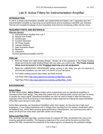
John CaldwellTI Designs – Precision: Verified DesignHeadphone Amplifier for Voltage-Output Audio DACsReference DesignTI Designs – PrecisionCircuit DescriptionTI Designs – Precision are analog solutions createdby TI’s analog experts. Verified Designs offer thetheory, component selection, simulation, completePCB schematic & layout, bill of materials, andmeasured performance of useful circuits. Circuitmodifications that help to meet alternate design goalsare also discussed.This headphone amplifier circuit converts the outputsignal from an audio digital-to-analog converter (DAC)into a single-ended signal suitable for headphones.An op amp is configured as a difference amplifier toconvert the differential output voltage from a DAC tosingle-ended. The circuit is designed to operate from5V bipolar power supplies commonly found inportable devices such as tablets and smartphones.Design ResourcesTIPD189TINA-TI OPA1688Ask The Analog ExpertsWEBENCH Design CenterTI Designs – Precision LibraryAll Design filesSPICE SimulatorProduct FolderC1R1R2ROUTVACVDC HeadphoneOutputVACROUTAudio DACR3R4C2An IMPORTANT NOTICE at the end of this TI reference design addresses authorized use, intellectual property matters andother important disclaimers and information.TINA-TI is a trademark of Texas InstrumentsWEBENCH is a registered trademark of Texas InstrumentsTIDUAW1-October 2015Headphone Amplifier for Voltage-Output Audio DACsCopyright 2015, Texas Instruments Incorporated1
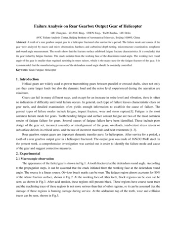
www.ti.com1Design SummaryThe design requirements are as follows: Supply Voltage: /-5 V Supply Current: 5mAThe design goals and performance are summarized in Table 1. Figure 1 depicts the measuredperformance of the design.Table 1: Comparison of Design Goals, Simulation, and Measured PerformanceGoalSimulatedMeasuredMagnitude Variation(20Hz – 20kHz)0.01dB0.009dB0.003dBPhase Variation(20Hz – 20kHz)5.0 0.927 -0.563ºTHD N (1kHz, 10mW,32 Ω load)-100dB (0.001%)-104.15dB (0.00062%)-106.7dB (0.00046%)Maximum OutputPower BeforeClipping (32 Ω)50mWN/A55mWOutput Impedance(1kHz) 0.1Ω0.00011Ω0.0317ΩTHD N vs Amplitude-401-500.1-70-800.01THD N (%)THD N tude (VRMS)32Ω16Ω1600ΩFigure 1: Measured THD N vs. Output Voltage2Headphone Amplifier for Voltage-Output Audio DACsCopyright 2015, Texas Instruments IncorporatedTIDUAW1-October 2015
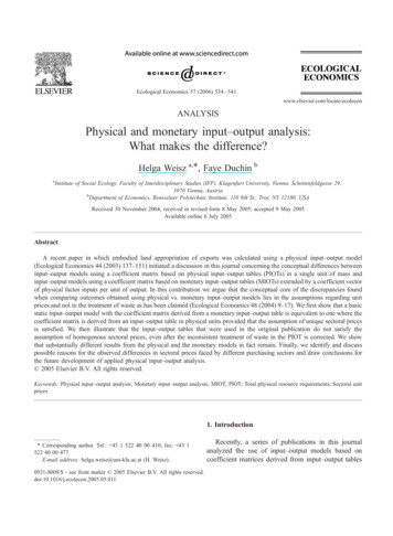
www.ti.com2Theory of OperationHigh performance audio DACs may have an output signal which is either a varying current or voltage.Additionally, “current segment” audio DACs may be used as a current output or a voltage output by simplychanging the external circuitry used with the DAC. Voltage output configurations require less externalcircuitry and therefore have advantages in cost, power consumption, and solution size. However, they mayoffer slightly lower performance than current output configurations. Differential outputs are standard onboth types of DACs because it doubles the output signal levels that can be delivered on a single, lowvoltage supply, and also allows for even-harmonics common to both outputs to be cancelled by externalcircuitry. A simplified representation of a voltage-output audio DAC is shown in Figure 2. Two ac voltagesources (VAC) deliver the output signal to the complementary outputs (OUT) through their associatedoutput impedances (ROUT). Both output signals may have a dc component as well, represented by dcvoltage source VDC.OUTROUT VACVDCVACROUTOUTAudio DACFigure 2: A simplified representation of a voltage output DACThe headphone amplifier circuit connected to the output of an audio DAC must convert the differentialoutput into a single-ended signal and be capable of producing signals of sufficient amplitude at theheadphones to achieve reasonable listening levels. Figure 3 shows a simplified schematic of a circuitwhich performs this function for voltage output DACs.C1R1R2ROUTVACVDC HeadphoneOutputVACROUTAudio DACR3R4C2Figure 3: A simplified schematic of a headphone amplifier circuit and audio DAC.An op amp is configured as a difference amplifier which converts the differential output voltage into asingle-ended one. The values of the resistors in the difference amplifier circuit are determined by thespecifications of the DAC such as output voltage and output impedance as well as the maximum outputvoltage desired at the headphone output. The op amp chosen must be capable of delivering the necessarycurrent to the headphones and remain stable into typical headphone loads which may have capacitancesas high as 400pF.TIDUAW1-October 2015Headphone Amplifier for Voltage-Output Audio DACsCopyright 2015, Texas Instruments Incorporated3
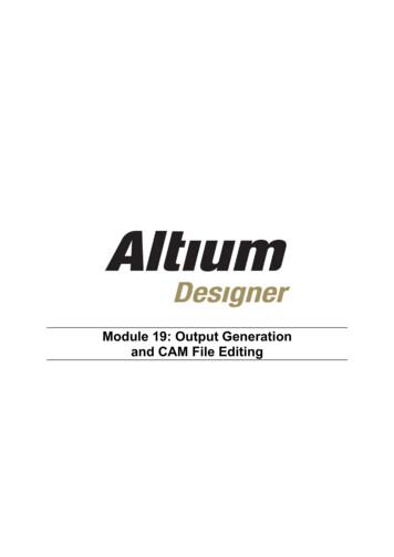
www.ti.com2.1Difference Amplifier DesignThe following design process will use a hypothetical DAC with common values of output voltage andimpedance for the design process. The specifications of the DAC are shown in Table 2.Table 2: Audio DAC specifications used for the design processParameterValueMax. differential output voltage2 VRMSOutput impedance (ROUT)300 ΩOutput dc offset1.65VThe gain of the difference amplifier in Figure 3 is determined by the resistor values and includes the outputimpedance of the DAC. For R2 R4 and R1 R3, the output voltage of the headphone amplifier circuit willbe:R2VOUT VDAC(1)R1 ROUTThe output voltage necessary for headphones depends on the headphone impedance as well as theheadphone efficiency, which is a measure of the sound pressure level (SPL, measured in dB) for a certaininput power level (typically given at 1mW). The headphone SPL at other power levels can be calculatedusing the efficiency at 1mW: P SPL(dB) 10 log IN 1mW (2)Where η is used to denote efficiency, and PIN is the input power to the headphones. Figure 4 shows theinput power required to produce certain SPLs for different headphone efficiencies. Typically, over-the-earstyle headphones have lower efficiencies than in-ear types with 95dB/mW being a common value.Sound Pressure Level vs. Input Power150140Sound Pressure Level (SPL, dB)13012090 dB/mW11095 dB/mW100100 dB/mW90105 dB/mW80110 dB/mW115 dB/mW70600.010.11101001000Input Power (mW)Figure 4: Sound pressure levels vs input power for headphones of varying sensitivity4Headphone Amplifier for Voltage-Output Audio DACsCopyright 2015, Texas Instruments IncorporatedTIDUAW1-October 2015
www.ti.comIn-ear headphones may have efficiencies of 115dB/mW or greater and will therefore have much lowerpower requirements. The output power goal for this design is 50mW which is sufficient power to produceextremely loud sound pressure levels in a wide range of headphones. A 32Ω headphone impedance isused for this requirement because this is a very common value in headphones for portable applications.The voltage required for 32 Ω headphones is therefore:VO P R 50mW 32 1.265VRMS(3)A tradeoff exists when selecting resistor values for this design. First, high resistor values contributeadditional noise to the circuit, degrading the audio performance. However, extremely low resistor valuesmay draw excessive current from the DAC, increasing distortion. A value of 2kΩ was selected for resistorsR1 and R3 as a reasonable compromise between these two considerations. Resistor R2 and R4 can thenbe calculated:R2R2VOUT VDAC 0.63 R2 1449 1.47k (4)R1 ROUT2k 300 The gain of the circuit can be increased to produce greater output voltages in order to accommodatehigher impedance headphones. However, this will increase the noise of the circuit, and will also limit thedynamic range of the circuit into lower impedance headphones. For this reason, some designers chose tohave the headphone amplifier gain selectable by a switch.2.2Capacitor SelectionCapacitors C1 and C2 have a dual role in the headphone amplifier circuit. First, they limit the bandwidth ofthe circuit to prevent the unnecessary amplification of interfering signals. Second, these capacitors canhelp to increase the overall stability of the circuit. The maximum value of these capacitors is determined bythe limitations on frequency response magnitude and phase deviations detailed in Section 1. C1 and C2combine with resistors R2 and R4 to form a pole at:fP 12 ( R2 , R4 )(C1 , C2 )(5)The phase shift at 20 kHz due to this pole should be limited to less than 5 ; this allows the pole frequencyto be calculated:fP f20kHz 228.6kHztan( ) tan(5 )(6)We must also calculate the minimum pole frequency allowable to meet the magnitude deviationrequirements:fP f2 1 1 G 20kHz2 1 1 0.999 416.6kHz(7)Where G represents the gain in decimal for a -0.01 dB deviation at 20 kHz, the upper limit for the value ofC1 and C2 can be calculated to meet the goals for phase shift and magnitude deviation at 20 kHz.11C1 , C 2 260 pF(8)2 ( R2 , R4 ) FP 2 (1.47k )( 416.6kHz )This limit defines the value of C1 and C2 in order to meet the goals for magnitude and phase deviationover the passband of the amplifier circuit. However, C1 and C2 also help improve stability of the circuit intocapacitive loads such as headphones. Determining the optimum value for these capacitors for stability isbest performed in simulation. Please see the stability portion of the simulation section for the finalcapacitor value.TIDUAW1-October 2015Headphone Amplifier for Voltage-Output Audio DACsCopyright 2015, Texas Instruments Incorporated5
www.ti.com3Component Selection3.1ResistorsThe resistors forming the difference amplifier (R1, R2, R3, and R4) should be precision 0.1% resistors forbest performance. Precision resistors maximize the common-mode rejection of the difference amplifierwhich can reduce dc offset at the headphone output and cancel even harmonic distortion from the DAC.Thin film resistors are also suggested for best audio performance.3.2CapacitorsAll capacitors that may have a substantial signal voltage across them (C1, C2) must be C0G/NP0 typeceramics. Other types of ceramic capacitors (X7R, X5R, etc.) will produce large amounts of distortion anddegrade the performance of the circuit. Please see references [1] and [2] for more information on thiseffect.3.3AmplifierThe basic amplifier requirements are given in Table 3. Additional op amp performance requirements whichwill impact the audio performance are described in the following sections.Table 3: Basic op amp requirementsRequirementChannelsPower Supply VoltagePower Supply CurrentValueUnit2- 10V 2.5 mA/Ch.Output Current and VoltageThe most difficult requirement to satisfy in the process of op amp selection is the output current capability.For this design, each op amp channel is required to deliver:P I 2R I 50mW 39.5mARMS 55.9mAP32 (9)This is a linear output current level, meaning the amplifier is not clipping or limited by its output short circuitcurrent protection. Because short circuit current is often the metric used for sorting op amps by outputcurrent capability, an op amp must be selected with a short circuit current much higher than 56mA.Furthermore the amplifier must be able to deliver this amount of current on the specified power supplies.This gives an output swing requirement of:VCC VOUT ( P ) 5V 2 1.265VRMS 3.21V( 10 )This means that the amplifier must be able to produce output voltages within 3.21V of its power supplieswhile delivering 55.9mAp current.NoiseThe noise of the op amp should be low enough to meet the design goals for total harmonic distortion andnoise. To achieve a THD N of -100dB the total noise of the circuit must be less than:VN ( RMS ) V f 106THD ( dB)20 0.566VRMS 10 100dB20 5.66 VRMSHeadphone Amplifier for Voltage-Output Audio DACsCopyright 2015, Texas Instruments Incorporated( 11 )TIDUAW1-October 2015
www.ti.comTo calculate the input voltage noise of the op amp, the noise gain of the circuit will be calculated as well asthe thermal noise contributions of the feedback resistors. Noise gain is always the gain measured from thenon-inverting input of the amplifier:GN 1 R21.47k 1 1.639ROUT R1300 2k ( 12 )From a noise perspective, the feedback resistors are in parallel, and the thermal noise contribution iscalculated from their equivalent resistance:e NR 4kT K ( R1 , R3 ROUT ) ( R2 , R4 )( 13 ) 4(1.381 10 23 )( 298 K )( 2k 300 ) (1.47k ) 3.84nV / HzFinally, calculating the required input voltage noise of the op amp involves taking the total allowable RMSnoise voltage and dividing it by the measurement bandwidth and noise gain. The noise contributions of thefeedback resistors are subtracted from that value. These operations are performed in squares and thesquare root is then taken of the final value because noise sources add as a root sum of squares.e N (OA)2 V N ( RMS ) f G BW N2 2e 2 5.66 VRMS 2 3.84nV / HzNR 22kHz (1.639) 2 2( 14 )e N (OA) 22.64nV / HzThe input voltage noise of the op amp must be less than 22.64nV/ Hz to meet the THD N goals for thisdesign. This analysis does not include distortion harmonics in the THD N analysis. Therefore an amplifiershould be selected with much lower noise than the calculated value to account for the additionaldegradation in THD N caused by the distortion harmonics. Additionally, the current noise of the op amp isnot included in this analysis. However, because the source impedance presented to the op amp inputs isfairly low (1.47kΩ 2.3kΩ 896.8Ω), current noise was not anticipated to be a significant contributor to thetotal output noise.Slew RateThe slew rate requirements of headphone amplifiers are extremely modest. The slew rate of a sinusoid isgiven by the equation:SR 2 f A( 15 )Where f is the frequency of the waveform and A is the amplitude, the maximum output signal is 1.265V RMSor 1.789VP. At 20 kHz, the accepted upper end of audibility, the slew rate will be:SR 2 (20kHz)(1.789Vp) 224.8V / s .2248V / s( 16 )Consider that for a DAC with a 192 kHz sample rate, the highest output frequency limited by the Nyquistsampling theorem is 96 kHz,
Figure 3 shows a simplified schematic of a circuit which performs this function for voltage output DACs. -V DC Audio DAC Headphone Out put R 1 2 R 3 R 4 R OUT R OUT AC V AC C 1 C 2 Figure 3: A simplified schematic of a headphone amplifier circuit and audio DAC. An op amp is configured as a difference amplifier which converts the differential output voltage into a single-ended one. The .