Transcription
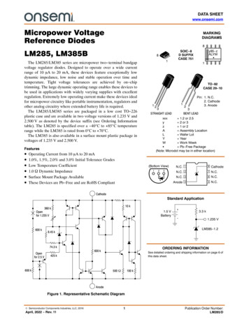
DATA SHEETwww.onsemi.comMicropower VoltageReference DiodesMARKINGDIAGRAMS8LM285, LM385BThe LM285/LM385 series are micropower two terminal bandgapvoltage regulator diodes. Designed to operate over a wide currentrange of 10 mA to 20 mA, these devices feature exceptionally lowdynamic impedance, low noise and stable operation over time andtemperature. Tight voltage tolerances are achieved by on chiptrimming. The large dynamic operating range enables these devices tobe used in applications with widely varying supplies with excellentregulation. Extremely low operating current make these devices idealfor micropower circuitry like portable instrumentation, regulators andother analog circuitry where extended battery life is required.The LM285/LM385 series are packaged in a low cost TO 226plastic case and are available in two voltage versions of 1.235 V and2.500 V as denoted by the device suffix (see Ordering Informationtable). The LM285 is specified over a 40 C to 85 C temperaturerange while the LM385 is rated from 0 C to 70 C.The LM385 is also available in a surface mount plastic package involtages of 1.235 V and 2.500 V.1Operating Current from 10 mA to 20 mA1.0%, 1.5%, 2.0% and 3.0% Initial Tolerance GradesLow Temperature Coefficient1.0 W Dynamic ImpedanceSurface Mount Package AvailableThese Devices are Pb Free and are RoHS Compliant1TO 92CASE 29 101123STRAIGHT LEAD2Pin: 1. N.C.2. Cathode3. Anode3BENT LEADxxx 1.2 or 2.5y 2 or 3z 1 or 2A Assembly LocationL Wafer LotY YearW Work WeekG Pb Free Package(Note: Microdot may be in either location)Features y85 zALYWGSOIC 8D SUFFIXCASE 7518(Bottom C.CathodeStandard Application10 k360 kOpenfor 1.235 V600 k1.5 VBattery-3.3 k1.235 VLM385 1.28.45 k74.3 kOpenfor 2.5 V ORDERING INFORMATION600 kSee detailed ordering and shipping information on page 6 ofthis data sheet.425 k500 W600 k100 kAnodeFigure 1. Representative Schematic Diagram Semiconductor Components Industries, LLC, 2016April, 2022 Rev. 111Publication Order Number:LM285/D
LM285, LM385BMAXIMUM RATINGS (TA 25 C, unless otherwise noted)RatingSymbolValueUnitReverse CurrentIR30mAForward CurrentIF10mAOperating Ambient Temperature RangeTALM285LM385 40 to 850 to 70 COperating Junction TemperatureTJ 150 CStorage Temperature RangeTstg 65 to 150 CElectrostatic Discharge Sensitivity (ESD)Human Body Model (HBM)Machine Model (MM)Charged Device Model (CDM)ESDV40004002000Stresses exceeding those listed in the Maximum Ratings table may damage the device. If any of these limits are exceeded, device functionalityshould not be assumed, damage may occur and reliability may be affected.ELECTRICAL CHARACTERISTICS (TA 25 C, unless otherwise noted)LM285 1.2CharacteristicSymbolReverse Breakdown Voltage (IRmin v IR v 20 mA)LM285 1.2/LM385B 1.2TA Tlow to Thigh (Note 1)LM385 1.2TA Tlow to Thigh (Note 1)V(BR)RMinimum Operating CurrentTA 25 CTA Tlow to Thigh (Note 1)Reverse Breakdown Voltage Change with CurrentIRmin v IR v 1.0 mA, TA 25 CTA Tlow to Thigh (Note 1)1.0 mA v IR v 20 mA, TA 25 CTA Tlow to Thigh (Note 1)Reverse Dynamic ImpedanceIR 100 mA, TA 25 CAverage Temperature Coefficient10 mA v IR v 20 mA, TA Tlow to Thigh (Note 1)MaxMinTypMax1.2231.200 1.235 1.2471.270 1.2231.2101.2051.1921.235 1.235 1.2471.2601.2601.273 8.0 1020 8.0 1520 1.01.51020 1.01.52025 0.6 0.6 80 80 60 60 20 20 2.4622.415 2.5 2.5382.585 2.4622.4362.4252.4002.5 2.5 2.5382.5642.5752.600 13 2030 13 2030mAmVDV(BR)/DTSUnitVZLong Term StabilityIR 100 mA, TA 25 C 0.1 C1. TlowThighTlowThighTypDV(BR)RnMinimum Operating CurrentTA 25 CTA Tlow to Thigh (Note 1)MinIRminWideband Noise (RMS)IR 100 mA, 10 Hz v f v 10 kHzReverse Breakdown Voltage (IRmin v IR v 20 mA)LM285 2.5/LM385B 2.5TA Tlow to Thigh (Note 1)LM385 2.5TA Tlow to Thigh (Note 1)LM385 1.2/LM385B 1.2Wppm/ CmVppm/kHRV(BR)RVIRmin 40 C for LM285 1.2, LM285 2.5 85 C for LM285 1.2, LM285 2.5 0 C for LM385 1.2, LM385B 1.2, LM385 2.5, LM385B 2.5 70 C for LM385 1.2, LM385B 1.2, LM385 2.5, LM385B 2.5www.onsemi.com2mA
LM285, LM385BELECTRICAL CHARACTERISTICS (TA 25 C, unless otherwise noted)LM285 1.2CharacteristicSymbolReverse Breakdown Voltage Change with CurrentIRmin v IR v 1.0 mA, TA 25 CTA Tlow to Thigh (Note 2)1.0 mA v IR v 20 mA, TA 25 CTA Tlow to Thigh (Note 2)DV(BR)RReverse Dynamic ImpedanceIR 100 mA, TA 25 CAverage Temperature Coefficient20 mA v IR v 20 mA, TA Tlow to Thigh (Note 2)TypMaxMinTypMax 1.01.51020 2.02.52025 0.6 0.6 80 80 120 120 20 20 Wppm/ CDV(BR)/DTnLong Term StabilityIR 100 mA, TA 25 C 0.1 CSUnitmVZWideband Noise (RMS)IR 100 mA, 10 Hz v f v 10 kHz2. TlowThighTlowThighLM385 1.2/LM385B 1.2MinmVppm/kHR 40 C for LM285 1.2, LM285 2.5 85 C for LM285 1.2, LM285 2.5 0 C for LM385 1.2, LM385B 1.2, LM385 2.5, LM385B 2.5 70 C for LM385 1.2, LM385B 1.2, LM385 2.5, LM385B 2.5www.onsemi.com3
LM285, LM385BΔV(BR)R, REVERSE VOLTAGE CHANGE (mV)TYPICAL PERFORMANCE CURVES FOR LM285 1.2/385 1.2/385B 1.2IR, REVERSE CURRENT ( A)μ10010TA 85 C1.0 25 C0.100.2- 40 C0.40.60.81.0V(BR), REVERSE VOLTAGE (V)1.21.4108.0TA 85 C6.0 25 C4.0- 40 C2.00-2.00.010.1Figure 2. Reverse Characteristics1.010IR, REVERSE CURRENT (mA)100Figure 3. Reverse Characteristics1.2V(BR)R, REVERSE VOLTAGE (V)VF, FORWARD VOLTAGE (V)1.2501.0TA - 40 C0.80.6 25 C 85 C0.40.200.011.2301.2201.2100.11.010IF , FORWARD CURRENT (mA)IR 100 mA1.240100-50Figure 4. Forward Characteristics1.501.25OUTPUT (V)750625500125Input100 k1.000.75Output0.50DUT0.253750250INPUT (V) Hz)100Figure 5. Temperature Drift875e n , NOISE (nV/-250255075TA , AMBIENT TEMPERATURE ( C)1250101001.0 Kf, FREQUENCY (Hz)10 K105.00100 kFigure 6. Noise Voltage00.10.20.30.6 0.7t, TIME (ms)0.80.9Figure 7. Response Timewww.onsemi.com41.01.1
LM285, LM385BΔV(BR)R, REVERSE VOLTAGE CHANGE (mV)TYPICAL PERFORMANCE CURVES FOR LM285 2.5/385 2.5/385B 2.5IR, REVERSE CURRENT ( A)μ10010TA 85 C 25 C1.0- 40 C0.100.51.01.52.02.5V(BR), REVERSE VOLTAGE (V)3.03.510TA 85 C8.06.0 25 C2.00-2.00.010.1Figure 8. Reverse CharacteristicsV(BR)R, REVERSE VOLTAGE (V)VF, FORWARD VOLTAGE (V)1.0TA - 40 C0.80.6 85 C 25 C0.200.012.5201.010IF , FORWARD CURRENT (mA)2.5002.4902.4802.4702.460100-50Figure 10. Forward Characteristics-250255075TA , AMBIENT TEMPERATURE ( C)100125Figure 11. Temperature Drift3.002.50 Hz)OUTPUT (V)150012501000Input100 k2.001.50Output1.00DUT0.507500500INPUT (V)e n , NOISE (nV/100IR 100 mA2.5102.4500.11.010IR, REVERSE CURRENT (mA)Figure 9. Reverse Characteristics1.20.4- 40 C4.02500101001.0 Kf, FREQUENCY (Hz)10 K105.00100 kFigure 12. Noise Voltage00.10.20.30.6 0.7t, TIME (ms)0.8Figure 13. Response Timewww.onsemi.com50.91.01.1
LM285, LM385BORDERING INFORMATIONDeviceOperating Temperature RangeReverse Break DownVoltageLM285D 1.2LM285D 1.2G1.235 VLM285D 1.2R2LM285D 1.2R2GLM285D 2.5LM285D 2.5G2.500 VLM285D 2.5R2LM285D 2.5R2GLM285Z 1.2LM285Z 1.2GTA 40 C to 85 C1.235 VLM285Z 2.52.500 VLM285Z 2.5GLM285Z 1.2RA1.235 VLM285Z 1.2RAGLM285Z 2.5RALM285Z 2.5RAG2.500 VLM285Z 2.5RPLM285Z 2.5RPGLM385BD 1.2LM385BD 1.2G1.235 VLM385BD 1.2R2LM385BD 1.2R2GLM385BD 2.5LM385BD 2.5GLM385BD 2.5R2TA 0 C to 70 C2.500 VLM385BD 2.5R2GLM385BZ 1.2LM385BZ 1.2GLM385BZ 1.2RA1.235 VLM385BZ 1.2RAGPackageShipping†SOIC 898 Units / RailSOIC 8(Pb Free)98 Units / RailSOIC 82500 / Tape & ReelSOIC 8(Pb Free)2500 / Tape & ReelSOIC 898 Units / RailSOIC 8(Pb Free)98 Units / RailSOIC 82500 / Tape & ReelSOIC 8(Pb Free)2500 / Tape & ReelTO 922000 Units / BagTO 92(Pb Free)2000 Units / BagTO 922000 Units / BagTO 92(Pb Free)2000 Units / BagTO 922000 / Tape & ReelTO 92(Pb Free)2000 / Tape & ReelTO 922000 / Tape & ReelTO 92(Pb Free)2000 / Tape & ReelTO 922000 Units / Fan FoldTO 92(Pb Free)2000 Units / Fan FoldSOIC 898 Units / RailSOIC 8(Pb Free)98 Units / RailSOIC 82500 / Tape & ReelSOIC 8(Pb Free)2500 / Tape & ReelSOIC 898 Units / RailSOIC 8(Pb Free)98 Units / RailSOIC 82500 / Tape & ReelSOIC 8(Pb Free)2500 / Tape & ReelTO 922000 Units / BagTO 92(Pb Free)2000 Units / BagTO 922000 / Tape & ReelTO 92(Pb Free)2000 / Tape & Reel†For information on tape and reel specifications, including part orientation and tape sizes, please refer to our Tape and Reel PackagingSpecifications Brochure, BRD8011/D.www.onsemi.com6
LM285, LM385BORDERING INFORMATIONDeviceOperating Temperature RangeReverse Break DownVoltageLM385BZ 2.5LM385BZ 2.5G2.500 VLM385BZ 2.5RALM385BZ 2.5RAGLM385D 1.2LM385D 1.2G1.235 VLM385D 1.2R2LM385D 1.2R2GLM385D 2.5LM385D 2.5G2.500 VLM385D 2.5R2LM385D 2.5R2GTA 0 C to 70 CLM385Z 1.2LM385Z 1.2GLM385Z 1.2RALM385Z 1.2RAG1.235 VLM385Z 1.2RPLM385Z 1.2RPGLM385Z 2.5LM385Z 2.5GLM385Z 2.5RP2.500 VLM385Z 2.5RPGPackageShipping†TO 922000 Units / BagTO 92(Pb Free)2000 Units / BagTO 922000 / Tape & ReelTO 92(Pb Free)2000 / Tape & ReelSOIC 898 Units / RailSOIC 8(Pb Free)98 Units / RailSOIC 82500 / Tape & ReelSOIC 8(Pb Free)2500 / Tape & ReelSOIC 898 Units / RailSOIC 8(Pb Free)98 Units / RailSOIC 82500 / Tape & ReelSOIC 8(Pb Free)2500 / Tape & ReelTO 922000 Units / BagTO 92(Pb Free)2000 Units / BagTO 922000 / Tape & ReelTO 92(Pb Free)2000 / Tape & ReelTO 922000 / Ammo BoxTO 92(Pb Free)2000 / Ammo BoxTO 922000 Units / BagTO 92(Pb Free)2000 Units / BagTO 922000 / Ammo BoxTO 92(Pb Free)2000 / Ammo Box†For information on tape and reel specifications, including part orientation and tape sizes, please refer to our Tape and Reel PackagingSpecifications Brochure, BRD8011/D.www.onsemi.com7
MECHANICAL CASE OUTLINEPACKAGE DIMENSIONSTO 92 (TO 226) 1 WATTCASE 29 10ISSUE DSCALE 1:1123STRAIGHT LEAD1DATE 05 MAR 202123BENT LEADSTYLES AND MARKING ON PAGE 3DOCUMENT NUMBER:DESCRIPTION:98AON52857ETO 92 (TO 226) 1 WATTElectronic versions are uncontrolled except when accessed directly from the Document Repository.Printed versions are uncontrolled except when stamped “CONTROLLED COPY” in red.PAGE 1 OF 3ON Semiconductor andare trademarks of Semiconductor Components Industries, LLC dba ON Semiconductor or its subsidiaries in the United States and/or other countries.ON Semiconductor reserves the right to make changes without further notice to any products herein. ON Semiconductor makes no warranty, representation or guarantee regardingthe suitability of its products for any particular purpose, nor does ON Semiconductor assume any liability arising out of the application or use of any product or circuit, and specificallydisclaims any and all liability, including without limitation special, consequential or incidental damages. ON Semiconductor does not convey any license under its patent rights nor therights of others. Semiconductor Components Industries, LLC, 2019www.onsemi.com
MECHANICAL CASE OUTLINEPACKAGE DIMENSIONSTO 92 (TO 226) 1 WATTCASE 29 10ISSUE DDATE 05 MAR 2021STYLES AND MARKING ON PAGE 3DOCUMENT NUMBER:DESCRIPTION:98AON52857ETO 92 (TO 226) 1 WATTElectronic versions are uncontrolled except when accessed directly from the Document Repository.Printed versions are uncontrolled except when stamped “CONTROLLED COPY” in red.PAGE 2 OF 3ON Semiconductor andare trademarks of Semiconductor Components Industries, LLC dba ON Semiconductor or its subsidiaries in the United States and/or other countries.ON Semiconductor reserves the right to make changes without further notice to any products herein. ON Semiconductor makes no warranty, representation or guarantee regardingthe suitability of its products for any particular purpose, nor does ON Semiconductor assume any liability arising out of the application or use of any product or circuit, and specificallydisclaims any and all liability, including without limitation special, consequential or incidental damages. ON Semiconductor does not convey any license under its patent rights nor therights of others. Semiconductor Components Industries, LLC, 2019www.onsemi.com
TO 92 (TO 226) 1 WATTCASE 29 10ISSUE DDATE 05 MAR 2021STYLE 1:PIN 1. EMITTER2. BASE3. COLLECTORSTYLE 2:PIN 1. BASE2. EMITTER3. COLLECTORSTYLE 3:PIN 1. ANODE2. ANODE3. CATHODESTYLE 4:PIN 1. CATHODE2. CATHODE3. ANODESTYLE 5:PIN 1. DRAIN2. SOURCE3. GATESTYLE 6:PIN 1. GATE2. SOURCE & SUBSTRATE3. DRAINSTYLE 7:PIN 1. SOURCE2. DRAIN3. GATESTYLE 8:PIN 1. DRAIN2. GATE3. SOURCE & SUBSTRATESTYLE 9:PIN 1. BASE 12. EMITTER3. BASE 2STYLE 10:PIN 1. CATHODE2. GATE3. ANODESTYLE 11:PIN 1. ANODE2. CATHODE & ANODE3. CATHODESTYLE 12:PIN 1. MAIN TERMINAL 12. GATE3. MAIN TERMINAL 2STYLE 13:PIN 1. ANODE 12. GATE3. CATHODE 2STYLE 14:PIN 1. EMITTER2. COLLECTOR3. BASESTYLE 15:PIN 1. ANODE 12. CATHODE3. ANODE 2STYLE 16:PIN 1. ANODE2. GATE3. CATHODESTYLE 17:PIN 1. COLLECTOR2. BASE3. EMITTERSTYLE 18:PIN 1. ANODE2. CATHODE3. NOT CONNECTEDSTYLE 19:PIN 1. GATE2. ANODE3. CATHODESTYLE 20:PIN 1. NOT CONNECTED2. CATHODE3. ANODESTYLE 21:PIN 1. COLLECTOR2. EMITTER3. BASESTYLE 22:PIN 1. SOURCE2. GATE3. DRAINSTYLE 23:PIN 1. GATE2. SOURCE3. DRAINSTYLE 24:PIN 1. EMITTER2. COLLECTOR/ANODE3. CATHODESTYLE 25:PIN 1. MT 12. GATE3. MT 2STYLE 26:PIN 1.2.3.STYLE 27:PIN 1. MT2. SUBSTRATE3. MTSTYLE 28:PIN 1. CATHODE2. ANODE3. GATESTYLE 29:PIN 1. NOT CONNECTED2. ANODE3. CATHODESTYLE 30:PIN 1. DRAIN2. GATE3. SOURCESTYLE 32:PIN 1. BASE2. COLLECTOR3. EMITTERSTYLE 33:PIN 1. RETURN2. INPUT3. OUTPUTSTYLE 34:PIN 1. INPUT2. GROUND3. LOGICSTYLE 35:PIN 1. GATE2. COLLECTOR3. EMITTERVCCGROUND 2OUTPUTSTYLE 31:PIN 1. GATE2. DRAIN3. SOURCEGENERICMARKING DIAGRAM*XXXXXXXXXXALYWGGXXXXALYWG Specific Device Code Assembly Location Wafer Lot Year Work Week Pb Free Package(Note: Microdot may be in either location)*This information is generic. Please refer todevice data sheet for actual part marking.Pb Free indicator, “G” or microdot “G”, mayor may not be present. Some products maynot follow the Generic Marking.DOCUMENT NUMBER:DESCRIPTION:98AON52857ETO 92 (TO 226) 1 WATTElectronic versions are uncontrolled except when accessed directly from the Document Repository.Printed versions are uncontrolled except when stamped “CONTROLLED COPY” in red.PAGE 3 OF 3ON Semiconductor andare trademarks of Semiconductor Components Industries, LLC dba ON Semiconductor or its subsidiaries in the United States and/or other countries.ON Semiconductor reserves the right to make changes without further notice to any products herein. ON Semiconductor makes no warranty, representation or guarantee regardingthe suitability of its products for any particular purpose, nor does ON Semiconductor assume any liability arising out of the application or use of any product or circuit, and specificallydisclaims any and all liability, including without limitation special, consequential or incidental damages. ON Semiconductor does not convey any license under its patent rights nor therights of others. Semiconductor Components Industries, LLC, 2019www.onsemi.com
MECHANICAL CASE OUTLINEPACKAGE DIMENSIONSSOIC 8 NBCASE 751 07ISSUE AK81SCALE 1:1 X DATE 16 FEB 2011NOTES:1. DIMENSIONING AND TOLERANCING PERANSI Y14.5M, 1982.2. CONTROLLING DIMENSION: MILLIMETER.3. DIMENSION A AND B DO NOT INCLUDEMOLD PROTRUSION.4. MAXIMUM MOLD PROTRUSION 0.15 (0.006)PER SIDE.5. DIMENSION D DOES NOT INCLUDE DAMBARPROTRUSION. ALLOWABLE DAMBARPROTRUSION SHALL BE 0.127 (0.005) TOTALIN EXCESS OF THE D DIMENSION ATMAXIMUM MATERIAL CONDITION.6. 751 01 THRU 751 06 ARE OBSOLETE. NEWSTANDARD IS 751 07.A85SB0.25 (0.010)MYM14 Y KGCNX 45SEATINGPLANE Z 0.10 (0.004)HMD0.25 (0.010)MZ YSXJS8811IC4.00.155XXXXXALYWGIC(Pb Free) Specific Device Code Assembly Location Wafer Lot Year Work Week Pb Free PackageXXXXXXAYWW11DiscreteXXXXXXAYWWGDiscrete(Pb Free)XXXXXX Specific Device CodeA Assembly LocationY YearWW Work WeekG Pb Free Package*This information is generic. Please refer todevice data sheet for actual part marking.Pb Free indicator, “G” or microdot “G”, mayor may not be present. Some products maynot follow the Generic Marking.1.2700.050SCALE 0.0200.050 METERSMINMAX4.805.003.804.001.351.750.330.511.27 ICMARKING DIAGRAM*SOLDERING FOOTPRINT*7.00.275DIMABCDGHJKMNSmm Ǔǒinches*For additional information on our Pb Free strategy and solderingdetails, please download the ON Semiconductor Soldering andMounting Techniques Reference Manual, SOLDERRM/D.STYLES ON PAGE 2DOCUMENT NUMBER:DESCRIPTION:98ASB42564BSOIC 8 NBElectronic versions are uncontrolled except when accessed directly from the Document Repository.Printed versions are uncontrolled except when stamped “CONTROLLED COPY” in red.PAGE 1 OF 2onsemi andare trademarks of Semiconductor Components Industries, LLC dba onsemi or its subsidiaries in the United States and/or other countries. onsemi reservesthe right to make changes without further notice to any products herein. onsemi makes no warranty, representation or guarantee regarding the suitability of its products for any particularpurpose, nor does onsemi assume any liability arising out of the application or use of any product or circuit, and specifically disclaims any and all liability, including without limitationspecial, consequential or incidental damages. onsemi does not convey any license under its patent rights nor the rights of others. Semiconductor Components Industries, LLC, 2019www.onsemi.com
SOIC 8 NBCASE 751 07ISSUE AKDATE 16 FEB 2011STYLE 1:PIN 1. EMITTER2. COLLECTOR3. COLLECTOR4. EMITTER5. EMITTER6. BASE7. BASE8. EMITTERSTYLE 2:PIN 1. COLLECTOR, DIE, #12. COLLECTOR, #13. COLLECTOR, #24. COLLECTOR, #25. BASE, #26. EMITTER, #27. BASE, #18. EMITTER, #1STYLE 3:PIN 1. DRAIN, DIE #12. DRAIN, #13. DRAIN, #24. DRAIN, #25. GATE, #26. SOURCE, #27. GATE, #18. SOURCE, #1STYLE 4:PIN 1. ANODE2. ANODE3. ANODE4. ANODE5. ANODE6. ANODE7. ANODE8. COMMON CATHODESTYLE 5:PIN 1. DRAIN2. DRAIN3. DRAIN4. DRAIN5. GATE6. GATE7. SOURCE8. SOURCESTYLE 6:PIN 1. SOURCE2. DRAIN3. DRAIN4. SOURCE5. SOURCE6. GATE7. GATE8. SOURCESTYLE 7:PIN 1. INPUT2. EXTERNAL BYPASS3. THIRD STAGE SOURCE4. GROUND5. DRAIN6. GATE 37. SECOND STAGE Vd8. FIRST STAGE VdSTYLE 8:PIN 1. COLLECTOR, DIE #12. BASE, #13. BASE, #24. COLLECTOR, #25. COLLECTOR, #26. EMITTER, #27. EMITTER, #18. COLLECTOR, #1STYLE 9:PIN 1. EMITTER, COMMON2. COLLECTOR, DIE #13. COLLECTOR, DIE #24. EMITTER, COMMON5. EMITTER, COMMON6. BASE, DIE #27. BASE, DIE #18. EMITTER, COMMONSTYLE 10:PIN 1. GROUND2. BIAS 13. OUTPUT4. GROUND5. GROUND6. BIAS 27. INPUT8. GROUNDSTYLE 11:PIN 1. SOURCE 12. GATE 13. SOURCE 24. GATE 25. DRAIN 26. DRAIN 27. DRAIN 18. DRAIN 1STYLE 12:PIN 1. SOURCE2. SOURCE3. SOURCE4. GATE5. DRAIN6. DRAIN7. DRAIN8. DRAINSTYLE 13:PIN 1. N.C.2. SOURCE3. SOURCE4. GATE5. DRAIN6. DRAIN7. DRAIN8. DRAINSTYLE 14:PIN 1. N SOURCE2. N GATE3. P SOURCE4. P GATE5. P DRAIN6. P DRAIN7. N DRAIN8. N DRAINSTYLE 15:PIN 1. ANODE 12. ANODE 13. ANODE 14. ANODE 15. CATHODE, COMMON6. CATHODE, COMMON7. CATHODE, COMMON8. CATHODE, COMMONSTYLE 16:PIN 1. EMITTER, DIE #12. BASE, DIE #13. EMITTER, DIE #24. BASE, DIE #25. COLLECTOR, DIE #26. COLLECTOR, DIE #27. COLLECTOR, DIE #18. COLLECTOR, DIE #1STYLE 17:PIN 1. VCC2. V2OUT3. V1OUT4. TXE5. RXE6. VEE7. GND8. ACCSTYLE 18:PIN 1. ANODE2. ANODE3. SOURCE4. GATE5. DRAIN6. DRAIN7. CATHODE8. CATHODESTYLE 19:PIN 1. SOURCE 12. GATE 13. SOURCE 24. GATE 25. DRAIN 26. MIRROR 27. DRAIN 18. MIRROR 1STYLE 20:PIN 1. SOURCE (N)2. GATE (N)3. SOURCE (P)4. GATE (P)5. DRAIN6. DRAIN7. DRAIN8. DRAINSTYLE 21:PIN 1. CATHODE 12. CATHODE 23. CATHODE 34. CATHODE 45. CATHODE 56. COMMON ANODE7. COMMON ANODE8. CATHODE 6STYLE 22:PIN 1. I/O LINE 12. COMMON CATHODE/VCC3. COMMON CATHODE/VCC4. I/O LINE 35. COMMON ANODE/GND6. I/O LINE 47. I/O LINE 58. COMMON ANODE/GNDSTYLE 23:PIN 1. LINE 1 IN2. COMMON ANODE/GND3. COMMON ANODE/GND4. LINE 2 IN5. LINE 2 OUT6. COMMON ANODE/GND7. COMMON ANODE/GND8. LINE 1 OUTSTYLE 24:PIN 1. BASE2. EMITTER3. COLLECTOR/ANODE4. COLLECTOR/ANODE5. CATHODE6. CATHODE7. COLLECTOR/ANODE8. COLLECTOR/ANODESTYLE 25:PIN 1. VIN2. N/C3. REXT4. GND5. IOUT6. IOUT7. IOUT8. IOUTSTYLE 26:PIN 1. GND2. dv/dt3. ENABLE4. ILIMIT5. SOURCE6. SOURCE7. SOURCE8. VCCSTYLE 29:PIN 1. BASE, DIE #12. EMITTER, #13. BASE, #24. EMITTER, #25. COLLECTOR, #26. COLLECTOR, #27. COLLECTOR, #18. COLLECTOR, #1STYLE 30:PIN 1. DRAIN 12. DRAIN 13. GATE 24. SOURCE 25. SOURCE 1/DRAIN 26. SOURCE 1/DRAIN 27. SOURCE 1/DRAIN 28. GATE 1DOCUMENT NUMBER:DESCRIPTION:98ASB42564BSOIC 8 NBSTYLE 27:PIN 1. ILIMIT2. OVLO3. UVLO4. INPUT 5. SOURCE6. SOURCE7. SOURCE8. DRAINSTYLE 28:PIN 1. SW TO GND2. DASIC OFF3. DASIC SW DET4. GND5. V MON6. VBULK7. VBULK8. VINElectronic versions are uncontrolled except when accessed directly from the Document Repository.Printed versions are uncontrolled except when stamped “CONTROLLED COPY” in red.PAGE 2 OF 2onsemi andare trademarks of Semiconductor Components Industries, LLC dba onsemi or its subsidiaries in the United States and/or other countries. onsemi reservesthe right to make changes without further notice to any products herein. onsemi makes no warranty, representation or guarantee regarding the suitability of its products for any particularpurpose, nor does onsemi assume any liability arising out of the application or use of any product or circuit, and specifically disclaims any and all liability, including without limitationspecial, consequential or incidental damages. onsemi does not convey any license under its patent rights nor the rights of others. Semiconductor Components Industries, LLC, 2019www.onsemi.com
onsemi,, and other names, marks, and brands are registered and/or common law trademarks of Semiconductor Components Industries, LLC dba “onsemi” or its affiliatesand/or subsidiaries in the United States and/or other countries. onsemi owns the rights to a number of patents, trademarks, copyrights, trade secrets, and other intellectual property.A listing of onsemi’s product/patent coverage may be accessed at www.onsemi.com/site/pdf/Patent Marking.pdf. onsemi reserves the right to make changes at any time to anyproducts or information herein, without notice. The information herein is provided “as is” and onsemi makes no warranty, representation or guarantee regarding the accuracy of theinformation, product features, availability, functionality, or suitability of its products for any particular purpose, nor does onsemi assume any liability arising out of the application or useof any product or circuit, and specifically disclaims any and all liability, including without limitation special, consequential or incidental damages. Buyer is responsible for its productsand applications using onsemi products, including compliance with all laws, regulations and safety requirements or standards, regardless of any support or applications informationprovided by onsemi. “Typical” parameters which may be provided in onsemi data sheets and/or specifications can and do vary in different applications and actual performance mayvary over time. All operating parameters, including “Typicals” must be validated for each customer application by customer’s technical experts. onsemi does not convey any licenseunder any of its intellectual property rights nor the rights of others. onsemi products are not designed, intended, or authorized for use as a critical component in life support systemsor any FDA Class 3 medical devices or medical devices with a same or similar classification in a foreign jurisdiction or any devices intended for implantation in the human body. ShouldBuyer purchase or use onsemi products for any such unintended or unauthorized application, Buyer shall indemnify and hold onsemi and its officers, employees, subsidiaries, affiliates,and distributors harmless against all claims, costs, damages, and expenses, and reasonable attorney fees arising out of, directly or indirectly, any claim of personal injury or deathassociated with such unintended or unauthorized use, even if such claim alleges that onsemi was negligent regarding the design or manufacture of the part. onsemi is an EqualOpportunity/Affirmative Action Employer. This literature is subject to all applicable copyright laws and is not for resale in any manner.PUBLICATION ORDERING INFORMATIONLITERATURE FULFILLMENT:Email Requests to: orderlit@onsemi.comonsemi Website: www.onsemi.com TECHNICAL SUPPORTNorth American Technical Support:Voice Mail: 1 800 282 9855 Toll Free USA/CanadaPhone: 011 421 33 790 2910Europe, Middle East and Africa Technical Support:Phone: 00421 33 790 2910For additional information, please contact your local Sales Representative
The LM285/LM385 series are micropower two terminal bandgap voltage regulator diodes. Designed to operate over a wide current range of 10 A to 20 mA, these devices feature exceptionally low dynamic impedance, low noise and stable operation over time and temperature. Tight voltage tolerances are achieved by on chip