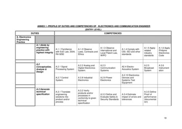
Transcription
Electronics, Inc.2590 North First Street, San Jose, CA 95131, U.S.A.Tel: 408-732-5000Fax: 408-732-5055http://www.atpinc.comRev. Date: Oct. 25, 2015ATP A4G16QE8BNPBSE16GB DDR4-2133 UNBUFFERED NON-ECC SODIMMDESCRIPTIONThe ATP A4G16QE8BNPBSE is a high performance 16GB DDR4-2133 Unbuffered NON-ECC SDRAMmemory module. It is organized as 2048M x 64 in a 260-pin Small Outline Dual-In-Line Memory Module(SODIMM) package. The module utilizes sixteen 1024Mx8 DDR4 SDRAMs in FBGA package. The moduleconsists of a 512-byte serial EEPROM, which contains the module configuration information.KEY FEATURES High Density: 16GB (2048M x 64)DIMM Rank: 2 RankCycle Time: 0.93ns (1067MHz)CAS Latency: 15Power supply: VDD 1.2V 0.06VVPP 2.5V 0.125VVDDSPD 2.2V 3.6VNominal and dynamic on-die termination(ODT) for data, strobe, and mask signalsLow-power auto self refresh (LPASR)Data bus inversion(DBI) for data bus16 internal banks(x8); 4 groups of 4 banks eachInternal self calibration through ZQTemperature controlled refresh (TCR)Asynchronous Reset7.8 s refresh interval at lower than TCASE85 C, 3.9 s refresh interval at 85 C TCASE 95 CSupport address and command signals parity functionSelectable BC4 or BL8 on-the fly(OTF)Dynamic On Die TerminationFly-by topologyFull module heat spreaderPCB Height: 1.18 inches(30mm)Minimum Thickness of Golden Finger: 30 Micro-inchRoHS compliantPart No.A4G16QE8BNPBSEMax Freq1067MHz (0.93ns@CL 15) x2Your Ultimate Memory Solution!Page 1 of 11InterfacePOD12
ATP A4G16QE8BNPBSEPIN DESCRIPTIONPin NameA0 A16A10/APA12/BC nBA0,BA1BG0,BG1RAS nCAS nWE nCS0 n, CS1 nCK0 t, CK1 tCK0 c, CK1 cCKE0, CKE1C0 C2ODT0, ODT1ACT nDQ0 DQ63DQS0 t DQS7 tDQS0 c DQS7 cDQM0 DQM7SCLSDASA0 SA2PARITYVDDVPPVREFCAVSSVDDSPDALERT nRESET nEVENT nVTTVDDQZQNCNFRFUDescriptionAddress InputsAddress Input/Auto prechargeAddress Input/Burst chopSDRAM Bank AddressBank group address inputsRow address strobe inputColumn address strobe inputWrite enable inputChip SelectsClock Inputs, positive lineClock Inputs, negative lineClock EnablesChip IDOn-die termination control lines inputCommand input: ACT n indicates an ACTIVATE command.Data Input /OutputData strobesData strobes, negative lineData MaskSerial clock for temperature sensor/SPD EEPROMSPD Data Input /OutputSerial address inputsParity for command and addressPower supplyDRAM activating power supplyReference voltage for control, command, and address pins.GroundSPD PowerAlert outputActive LOW asynchronous resetTemperature sensor Event OutputSDRAM I/O termination supplyDRAM DQ power supplyReference ball for ZQ calibrationNo ConnectNo functionReserved for future useYour Ultimate Memory Solution!2590 North First Street, San Jose, CA 95131, USA. http://www.atpinc.comTel. (408) 732-5000 Fax (408) 732-5055Page 2 of 11
ATP A4G16QE8BNPBSEPIN onNo.Designation1VSS2VSS133A1134EVENT n3DQ54DQ4135VDD136VDD5VSS6VSS137CK0 t138CK1 t7DQ18DQ0139CK0 c140CK1 c9VSS10VSS141VDD142VDD11DQS0 c12DQM0143PARITY144A013DQS0 VDDKEY19VSS20DQ2149CS0 n150BA021DQ322VSS151WE n /A14152RAS AS n/A1527VSS28DQ8157CS1 n158A1329DQ930VSS159VDD160VDD31VSS32DQS1 c161ODT1162C0,CS2 n,NC33DQM134DQS1 t163VDD164VREFCA35VSS36VSS165NC,CS3 74DQ3245DQ2146DQ20175VSS176VSS47VSS48VSS177DQS4 c178DQM449DQ1750DQ16179DQS4 t180VSS51VSS52VSS181VSS182DQ3953DQS2 c54DQM2183DQ38184VSS55DQS2 197VSS198DQS5 c69VSS70DQ24199DQM5200DQS5 t71DQ2572VSS201VSS202VSS73VSS74DQS3 c203DQ46204DQ4775DQM376DQS3 t205VSS206VSS77VSS78VSS207DQ42208DQ43Your Ultimate Memory Solution!2590 North First Street, San Jose, CA 95131, USA. http://www.atpinc.comTel. (408) 732-5000 Fax (408) 732-5055Page 3 of 11
ATP QS6 c220DQM691NC92NC221DQS6 06VSS235VSS236DQ57107VSS108RESET n237DQ56238VSS109CKE0110CKE1239VSS240DQS7 c111VDD112VDD241DQM7242DQS7 t113BG1114ACT n243VSS244VSS115BG0116ALERT n245DQ62246DQ63117VDD118VDD247VSS248VSS119A12/BC te:1. VPP is 2.5V DCYour Ultimate Memory Solution!2590 North First Street, San Jose, CA 95131, USA. http://www.atpinc.comTel. (408) 732-5000 Fax (408) 732-5055Page 4 of 11
ATP A4G16QE8BNPBSEFUNCTIONAL BLOCK DIAGRAM (PART1 OF 2)Your Ultimate Memory Solution!2590 North First Street, San Jose, CA 95131, USA. http://www.atpinc.comTel. (408) 732-5000 Fax (408) 732-5055Page 5 of 11
ATP A4G16QE8BNPBSEFUNCTIONAL BLOCK DIAGRAM (PART2 OF 2)Your Ultimate Memory Solution!2590 North First Street, San Jose, CA 95131, USA. http://www.atpinc.comTel. (408) 732-5000 Fax (408) 732-5055Page 6 of 11
ATP A4G16QE8BNPBSEABSOLUTE MAXIMUM DC RATINGSItemVoltage on VDD pin relative to VSSVoltage on VDDQ pin relative to VSSVoltage on VPP pin relative to VSSVoltage on any pin relative to VSSStorage TemperatureOperating TemperatureSymbolVDDVDDQVPPVIN, VOUTTSTGTCASERating-0.4V 1.5V-0.4V 1.5V-0.4V 3.0V-0.4V 1.975V-55 to 1000 to 95UnitsVVVVoCoCNotes1,31,3411,21,2Note:1. Stresses greater than those listed under “Absolute Maximum Ratings” may cause permanent damage to the device. This is a stress rating only and functionaloperation of the device at these or any other conditions above those indicated in the operational sections of this specification is not implied. Exposure to absolutemaximum rating conditions for extended periods may affect reliability2. Storage Temperature is the case surface temperature on the center/top side of the DRAM. For the measurement conditions, please refer to JESD51-2 standard.3. VDD and VDDQ must be within 300 mV of each other at all times;and VREFCA must be not greater than 0.6 x VDDQ, When VDD and VDDQ are less than 500 mV;VREFCA may be equal to or less than 300 mV4. VPP must be equal or greater than VDD/VDDQ at all times.AC & DC OPERATING CONDITIONSRecommended operating conditionsItemSupply Voltage 1,2,3Supply Voltage for Output 1,2,3DRAM Activating Power Supply3Input reference voltage command/address busTermination reference voltage (DC) –command/address bus4Input High Voltage (DC)Input High Voltage (AC)Input Low Voltage (DC)Input Low Voltage 9 * VDDTypical1.21.22.50.50 * VDDMax.1.261.262.750.51 * VDDUnitsVVVVVTT0.49 * VDD20mAVREF 0.075VREF 0.1VSS-0.50 * VDD0.51 * VDD 20mAVDDVREF - 0.075VREF - 0.1VVIH (DC)VIH (AC)VIL (DC)VIL (AC)-Note:1. Under all conditions VDDQ must be less than or equal to VDD.2. VDDQ tracks with VDD. AC parameters are measured with VDD and VDDQ tied together.3. DC bandwidth is limited to 20MHz.4. VTT termination voltages in excess of specification limit will adversely affect command and address signals' voltage margins, and reduce timing margins.RELIABILITYMTBF @25 oC (Hours) 1FIT @ 25 oC 2MTBF @40 oC (Hours) 1FIT @ 40 oC2TBDTBDTBDTBDNote:1. The Mean Time between Failures (MTBF) is calculated using a prediction methodology, Bellcore Prediction, which based on reliability data of the individualcomponents in the module. It assumes nominal voltage, with all other parameters within specified range.2. Failures per Billion Device-HoursYour Ultimate Memory Solution!2590 North First Street, San Jose, CA 95131, USA. http://www.atpinc.comTel. (408) 732-5000 Fax (408) 732-5055Page 7 of 11VVVV
ATP A4G16QE8BNPBSEIDD SPECIFICATION PARAMETER & POWER CONSUMPTION (PART1 OF 2)Values are for the DDR4 SDRAM only and are computed from values specified in the vendor’s component data sheet)SymbolProposed 40mA470mA48mA340mA1,000mAOperating One Bank Active-Precharge Current (AL 0)IDD0IPP0CKE: High; External clock: On; tCK, nRC, nRAS, CL: Refer to Component Datasheet for detail pattern; BL: 81; AL: 0; CS n: Highbetween ACT and PRE; Command, Address, Bank Group Address, Bank Address Inputs: partially toggling; Data IO: VDDQ; DM n:stable at 1; Bank Activity: Cycling with one bank active at a time: 0,0,1,1,2,2,. ; Output Buffer and RTT: Enabled in ModeRegisters2; ODT Signal: stable at 0; Pattern Details: Refer to Component Datasheet for detail patternOperating One Bank Active-Precharge IPP CurrentSame condition with IDD0Operating One Bank Active-Read-Precharge Current (AL 0)IDD1CKE: High; External clock: On; tCK, nRC, nRAS, nRCD, CL: Refer to Component Datasheet for detail pattern; BL: 81; AL: 0; CS n:High between ACT, RD and PRE; Command, Address, Bank Group Address, Bank Address Inputs, Data IO: partially toggling;DM n: sta-ble at 1; Bank Activity: Cycling with one bank active at a time: 0,0,1,1,2,2,. ; Output Buffer and RTT: Enabled in ModeRegisters2; ODT Signal: stable at 0; Pattern Details: Refer to Component Datasheet for detail patternPrecharge Standby Current (AL 0)IDD2NCKE: High; External clock: On; tCK, CL: Refer to Component Datasheet for detail pattern; BL: 81; AL: 0; CS n: stable at 1;Command, Address, Bank Group Address, Bank Address Inputs: partially toggling ; Data IO: VDDQ; DM n: stable at 1; BankActivity: all banks closed; Output Buffer and RTT: Enabled in Mode Registers2; ODT Signal: stable at 0; Pattern Details: Refer toComponent Datasheet for detail patternPrecharge Standby ODT CurrentIDD2NTCKE: High; External clock: On; tCK, CL: Refer to Component Datasheet for detail pattern; BL: 81; AL: 0; CS n: stable at 1;Command, Address, Bank Group Address, Bank Address Inputs: partially toggling ; Data IO: VSSQ; DM n: stable at 1; BankActivity: all banks closed; Output Buffer and RTT: Enabled in Mode Registers2; ODT Signal: toggling according ; Pattern Details:Refer to Component Datasheet for detail patternPrecharge Power-Down CurrentIDD2PCKE: Low; External clock: On; tCK, CL: Refer to Component Datasheet for detail pattern; BL: 81; AL: 0; CS n: stable at 1;Command, Address, Bank Group Address, Bank Address Inputs: stable at 0; Data IO: VDDQ; DM n: stable at 1; Bank Activity: allbanks closed; Output Buffer and RTT: Enabled in Mode Registers2; ODT Signal: stable at 0IDD2QCKE: High; External clock: On; tCK, CL: Refer to Component Datasheet for detail pattern; BL: 81; AL: 0; CS n: stable at 1;Command, Address, Bank Group Address, Bank Address Inputs: stable at 0; Data IO: VDDQ; DM n: stable at 1;Bank Activity: allbanks closed; Output Buffer and RTT: Enabled in Mode Registers2; ODT Signal: stable at 0Precharge Quiet Standby CurrentActive Standby CurrentIDD3NIPP3NCKE: High; External clock: On; tCK, CL: Refer to Component Datasheet for detail pattern; BL: 81; AL: 0; CS n: stable at 1;Command, Address, Bank Group Address, Bank Address Inputs: partially toggling ; Data IO: VDDQ; DM n: stable at 1;BankActivity: all banks open; Output Buffer and RTT: Enabled in Mode Registers2; ODT Signal: stable at 0; Pattern Details:Refer toComponent Datasheet for detail patternActive Standby IPP CurrentSame condition with IDD3NActive Power-Down CurrentIDD3PCKE: Low; External clock: On; tCK, CL: sRefer to Component Datasheet for detail pattern; BL: 81; AL: 0; CS n: stable at 1;Command, Address, Bank Group Address, Bank Address Inputs: stable at 0; Data IO: VDDQ; DM n: stable at 1; Bank Activity: allbanks open; Output Buffer and RTT: Enabled in Mode Registers2; ODT Signal: stable at 0Operating Burst Read CurrentIDD4RCKE: High; External clock: On; tCK, CL: Refer to Component Datasheet for detail pattern; BL: 82; AL: 0; CS n: High between RD;Command, Address, Bank Group Address, Bank Address Inputs: partially toggling ; Data IO: seamless read data burst with differentdata between one burst and the next one according ; DM n: stable at 1; Bank Activity: all banks open, RD commands cyclingthrough banks: 0,0,1,1,2,2,. ; Output Buffer and RTT: Enabled in Mode Registers2; ODT Signal: stable at 0; Pattern Details: Referto Component Datasheet for detail patternYour Ultimate Memory Solution!2590 North First Street, San Jose, CA 95131, USA. http://www.atpinc.comTel. (408) 732-5000 Fax (408) 732-5055Page 8 of 11
ATP A4G16QE8BNPBSEIDD SPECIFICATION PARAMETER & POWER CONSUMPTION (PART2 OF 2)Values are for the DDR4 SDRAM only and are computed from values specified in the vendor’s component data sheet)SymbolProposed mA360mA1,540mA88mAOperating Burst Write CurrentIDD4WCKE: High; External clock: On; tCK, CL: Refer to Component Datasheet for detail pattern; BL: 81; AL: 0; CS n: High between WR;Command, Address, Bank Group Address, Bank Address Inputs: partially toggling ; Data IO: seamless write data burst with differentdata between one burst and the next one ; DM n: stable at 1; Bank Activity: all banks open, WR commands cycling through banks:0,0,1,1,2,2,. ; Output Buffer and RTT: Enabled in Mode Registers2; ODT Signal: stable at HIGH; Pattern Details: Refer toComponent Datasheet for detail patternBurst Refresh Current (1X REF)IDD5BIPP5BCKE: High; External clock: On; tCK, CL, nRFC: Refer to Component Datasheet for detail pattern; BL: 81; AL: 0; CS n: Highbetween REF; Command, Address, Bank Group Address, Bank Address Inputs: partially toggling ; Data IO: VDDQ; DM n: stable at1; Bank Activity: REF command every nRFC ; Output Buffer and RTT: Enabled in Mode Registers2; ODT Signal: stable at 0; PatternDetails: Refer to Component Datasheet for detail patternBurst Refresh Write IPP Current (1X REF)Same condition with IDD5BSelf Refresh Current: Normal Temperature RangeIDD6NTCASE: 0 - 85 C; Low Power Array Self Refresh (LP ASR) : Normal4; CKE: Low; External clock: Off; CK t and CK c#: LOW; CL:Refer to Component Datasheet for detail pattern; BL: 81; AL: 0; CS n#, Command, Address, Bank Group Address, Bank Address,Data IO: High; DM n: stable at 1; Bank Activity: Self-Refresh operation; Output Buffer and RTT: Enabled in Mode Registers2; ODTSignal: MID-LEVELSelf-Refresh Current: Extended Temperature Range)IDD6ETCASE: 0 - 95 C; Low Power Array Self Refresh (LP ASR) : Extended4; CKE: Low; External clock: Off; CK t and CK c: LOW; CL:Refer to Component Datasheet for detail pattern; BL: 81; AL: 0; CS n, Command, Address, Bank Group Address, Bank Address,Data IO: High; DM n:stable at 1; Bank Activity: Extended Temperature Self-Refresh operation; Output Buffer and RTT: Enabled inMode Registers2; ODT Signal: MID-LEVELSelf-Refresh Current: Reduced Temperature RangeIDD6RTCASE: 0 - TBD ( 35-45) C; Low Power Array Self Refresh (LP ASR) : Reduced4; CKE: Low; External clock: Off; CK t and CK c#:LOW; CL: Refer to Component Datasheet for detail pattern; BL: 81; AL: 0; CS n#, Command, Address, Bank Group Address, BankAddress, Data IO: High; DM n:stable at 1; Bank Activity: Extended Temperature Self-Refresh operation; Output Buffer and RTT:Enabled in Mode Registers2; ODT Signal: MID-LEVELAuto Self-Refresh CurrentIDD6ATCASE: 0 - 95 C; Low Power Array Self Refresh (LP ASR) : Auto4;Partial Array Self-Refresh (PASR): Full Array; CKE: Low;External clock: Off; CK t and CK c#: LOW; CL: Refer to Component Datasheet for detail pattern; BL: 81; AL: 0; CS n#, Command,Address, Bank Group Address, Bank Address, Data IO: High; DM n:stable at 1; Bank Activity: Auto Self-Refresh operation; OutputBuffer and RTT: Enabled in Mode Registers2; ODT Signal: MID-LEVELOperating Bank Interleave Read CurrentIDD7CKE: High; External clock: On; tCK, nRC, nRAS, nRCD, nRRD, nFAW, CL: Refer to Component Datasheet for detail pattern; BL:81; AL: CL-1; CS n: High between ACT and RDA; Command, Address, Bank Group Address, Bank Address Inputs: partiallytoggling ; Data IO: read data bursts with different data between one burst and the next one ; DM n: stable at 1; Bank Activity: twotimes interleaved cycling through banks (0, 1, .7) with different addressing; Output Buffer and RTT: Enabled in Mode Registers2;ODT Signal: stable at 0; Pattern Details: Refer to Component Datasheet for detail patternIPP7Operating Bank Interleave Read IPP CurrentIDD8Maximum Power Down Current180mAPower Consumption per DIMM2,320mWPDIMMSame condition with IDD7System is operating at 1067MHz clock with VDD 1.2V. This parameter is calculated at a common loading.Your Ultimate Memory Solution!2590 North First Street, San Jose, CA 95131, USA. http://www.atpinc.comTel. (408) 732-5000 Fax (408) 732-5055Page 9 of 11
ATP A4G16QE8BNPBSETIMING PARAMETERParameterSymbolClock cycle time at CL 15, CWL 11Internal read command to first dataACT to internal read or write delay timePRE command periodACT to ACT or REF command periodACTIVE to PRECHARGE command periodAverage clock high pulse widthAverage clock low pulse widthDQS, DQS to DQ skew, per group, per accessDQ output hold time from DQS, DQSDQ low-impedance time from CK, CKDQ high-impedance time from CK, CKDQS, DQS READ PreambleDQS, DQS differential READ PostambleDQS, DQS output high timeDQS, DQS output low timeDQS, DQS WRITE PreambleDQS, DQS WRITE PostambleDQS, DQS low-impedance time (Referenced from RL-1)DQS, DQS high-impedance time (Referenced from RL BL/2)DQS, DQS differential input low pulse widthDQS, DQS differential input high pulse widthDQS, DQS rising edge to CK, CK rising edgeDQS, DQS falling edge setup time to CK, CK rising edgeDQS, DQS falling edge hold time to CK, CK rising edgeDDR4-2133MinMaxDLL locking timeInternal READ Command to PRECHARGE Command delayDelay from start of internal write trans-action to internal read command for different bank groupDelay from start of internal write trans-action to internal read command for same bank groupWRITE recovery timeMode Register Set command cycle timeMode Register Set command update delayCAS to CAS command delay for same bank groupAuto precharge write recovery precharge timeMulti-Purpose Register Recovery TimeACTIVE to ACTIVE command delay to same bank group for 1KB page sizeFour activate window for 1KB page sizeCommand and Address setup time to CK, CK referenced to Vih(ac) / Vil(ac) levelsCommand and Address hold time from CK, CK referenced to Vih(ac) / Vil(ac) levelsPower-up and RESET calibration timeNormal operation Full calibration timeNormal operation short calibration Z(DQS)tDQSLtDQSHtDQSStDSStDSHtDLLKtRTPtWTR StWTR )tZQinittZQopertZQCSExit Reset from CKE HIGH to a valid commandtXPRExit Power Down with DLL on to any valid command; Exit Precharge Power Down with DLLfrozen to commands not requiring a locked DLLAsynchronous RTT turn-on delay (Power-Down with DLL frozen)Asynchronous RTT turn-off delay (Power-Down with DLL frozen)RTT dynamic change skew8Gb REFRESH to REFRESH OR REFRESH to ACTIVE command intervalAverage periodic refresh interval (0 C TCASE 85 C)Average periodic refresh interval (85 C TCASE 95 C)Exit Self Refresh to commands not requiring a locked DLLExit Self Refresh to commands requiring a locked DLLPower Down Entry to Exit TimingWrite leveling output delayWrite leveling output errorNote:1. Unit ’nCK’ represents one clock cycle of the input clock, counting the actual clock EFItXStXSDLLtPDtWLOtWLOE110.33507.83.9tRFC(min) DYour Ultimate Memory Solution!2590 North First Street, San Jose, CA 95131, USA. http://www.atpinc.comTel. (408) 732-5000 Fax (408) 732-5055Page 10 of 110.938 5ns)6tWR roundup (tRP / max (5nCK,tRFC( min) nCK1nCK1nCK1nsnstCKnsususnCK1tCKnsns
ATP A4G16QE8BNPBSEPHYSICAL DIMENSIONS (UNITS IN INCHES)(Drawing not to scale)Note: Tolerance on all dimensions 0.006 inch (0.15mm) unless otherwise notedDisclaimer:No part of this document may be copied or reproduced in any form or by any means, or transferred to any third party,without the prior written consent of an authorized representative of ATP Electronics (“ATP”). The information in thisdocument is subject to change without notice. ATP assumes no responsibility for any errors or omissions that may appearin this document, and disclaims responsibility for any consequences resulting from the use of the information set forthherein. ATP makes no commitments to update or to keep current information contained in this document. Theinformation set forth in this document is considered to be “Proprietary” and “Confidential” property owned by ATP.Your Ultimate Memory Solution!2590 North First Street, San Jose, CA 95131, USA. http://www.atpinc.comTel. (408) 732-5000 Fax (408) 732-5055Page 11 of 11
consists of a 512-byte serial EEPROM, which contains the module configuration information. KEY FEATURES High Density: 16GB (2048M x 64) DIMM Rank: 2 Rank Cycle Time: 0.93ns (1067MHz) CAS Latency: 15 . 1 VSS 2 VSS 133 A1 134 EVENT_n 3 DQ5 4 DQ4 135 VDD 136 VDD 5 VSS 6 VSS 137 CK0_t 138 CK1_t 7 DQ1 8 DQ0 139 CK0_c 140 CK1_c 9 VSS 10 VSS 141 VDD .


![History of Electronics electricity [Read-Only]](/img/18/history-20of-20electronics-20-20electricity.jpg)
