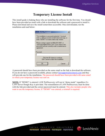
Transcription
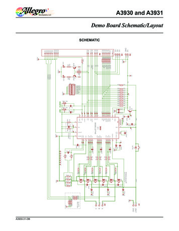
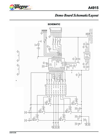
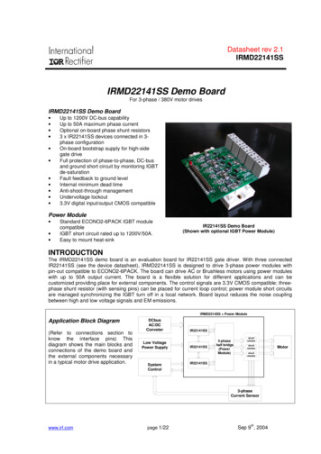
Datasheet rev 2.1IRMD22141SSIRMD22141SS Demo BoardFor 3-phase / 380V motor drivesIRMD22141SS Demo Board Up to 1200V DC-bus capabilityUp to 50A maximum phase currentOptional on-board phase shunt resistors3 x IR22141SS devices connected in 3phase configurationOn-board bootstrap supply for high-sidegate driveFull protection of phase-to-phase, DC-busand ground short circuit by monitoring IGBTde-saturationFault feedback to ground levelInternal minimum dead timeAnti-shoot-through managementUndervoltage lockout3.3V digital input/output CMOS compatiblePower Module Standard ECONO2-6PACK IGBT modulecompatibleIGBT short circuit rated up to 1200V/50A.Easy to mount heat-sinkIR22141SS Demo Board(Shown with optional IGBT Power Module)INTRODUCTIONThe IRMD22141SS demo board is an evaluation board for IR22141SS gate driver. With three connectedIR22141SS (see the device datasheet), IRMD22141SS is designed to drive 3-phase power modules withpin-out compatible to ECONO2-6PACK. The board can drive AC or Brushless motors using power moduleswith up to 50A output current. The board is a flexible solution for different applications and can becustomized providing place for external components. The control signals are 3.3V CMOS compatible; threephase shunt resistor (with sensing pins) can be placed for current loop control; power module short circuitsare managed synchronizing the IGBT turn off in a local network. Board layout reduces the noise couplingbetween high and low voltage signals and EM emissions.IRMD2214SS Power ModuleApplication Block Diagram(Refer to connections section toknow the interface pins) Thisdiagram shows the main blocks andconnections of the demo board andthe external components necessaryin a typical motor drive application.DCbusAC/DCConveterLow VoltagePower SupplySystemControlIR22141SSIR22141SS3-phasehalf resistorIR22141SS3-phaseCurrent Sensorwww.irf.compage 1/22thSep 9 , 2004Motor
Datasheet rev 2.1IRMD22141SSTable of contentsINTRODUCTION .1Table of contents.2Table of figures .2The IR22141SS.3The power module .3Important Notice.3BOARD CONNECTORS .4Connection with the system controller .4FAULT/SD logic signal .5VCC supply pin .5VSS ground pin (GND).5Connecting the current sensors .5High power signal connector.6Connecting the power module .6Test Points .7TEST BENCH CONNECTION .7OPERATING DESCRIPTION.8Power on sequence .8Normal operating mode.8Fault management .8Multilevel board solution.9BOARD SOLUTIONS.10Bootstrap circuit .10Gate resistances .10OTHER EXTRA COMPONENTS .11Desat circuit .11Clamping Diode for Vs below ground .11RC filter on com pin.12Fast diode between gate and supply pin .13Zener diode to preserve the IGBT gate .13Optional output shunt resistor .14Resistor on vcc .14BILL OF MATERIAL .15SCHEMATIC .16LAYOUT .16LAYOUT .17Table of figuresFigure 1: TOP image of board .4Figure 2: LED connection .5Figure 3: Test bench connection .7Figure 4: Power on sequence.8Figure 5: Three phase connection.9Figure 6: Example of a desaturation detection event .9Figure 7: Bootstrap circuit.10Figure 8: Desat external filter .11Figure 9: -Vs clamp .12Figure 10: COM below ground protection.12Figure 11: Collector-Gate current protection .13Figure 12: Zener clamp for IGBT gate.13www.irf.compage 2/22thSep 9 , 2004
Datasheet rev 2.1IRMD22141SSParametersValuesInput PowerDC 0 to 1200VDC-groundVcc15V typVssIccground100 mAOutput PowerIlmaxDCBus voltage positivewith 1200V power moduleDCbus voltage negativeLow voltage power supply.Follow IR22141 datasheetfor supply settingLow voltage groundquiescent Vcc current50A @25Cmax phase dc outputcurrent3.3V to 15V compatiblesee “Board Connectors”section on page 4Control Inputs/Outputs40 pin connector J1 I/OsDescription, conditionThe IR22141SSThe IR22141SS is a half bridge gate driver suited for power switching applications. The high side drivercan float up to 1200V. The IR22141SS have a high gate driving capability (2A source and 3A sink) witha low quiescent current. The device is designed to manage all the half-bridge faults by turning offsmoothly the desaturated transistor through the dedicated soft shut down pin preventing over-voltagesand reducing EM emissions. In a multi-phase system the drivers communicate using a dedicated localnetwork (SY FLT and FAULT/SD signals) to properly manage phase-to-phase short circuits. Thesystem controller may force shutdown or read device fault state through the 3.3 V compatible CMOS I/Opin (FAULT/SD). To improve the signal immunity from DC-bus noise, the control and power ground usededicated pins enabling low-side emitter current sensing as well. Undervoltage conditions in floating andlow voltage circuits are managed independently.For further technical information see the IR2214/IR22141 datasheet at http://www.irf.com.The power moduleIRMD22141SS demo board is ECONO2 compatible withSixPack standard pin out.Important NoticeIRMD22141SS demo board is supplied with a Bill Of Materialsuitable for a 1200V/50A@100C power module. The BOMpresented on page 15 provides a suggestion for the abovementioned power module.It is strongly recommended to customize the demo board to fit the application requirements for thepower module that has been chosen.Suggestions on passive sizing are also present in “Design Tips: Using monolithic high voltage gatedrivers”.www.irf.compage 3/22thSep 9 , 2004
Datasheet rev 2.1IRMD22141SSBOARD CONNECTORSP1P2J1P3Figure 1: TOP image of boardConnection with the system controllerOn board there is a 40 pins connector for the control signals. The driver board uses only 17 pins. Theremaining pins are for the sensing board (IRCS2277S) that can be connected on top of IRMD22141SSboard.CONNECTOR 417181920212223242526LIN32556FLT CLR327282930FAULT/SD5/631323334353637383940VCC37 - 40VSS17 - 20Table 1: 40-pin connector J1Input logical signals HIN1, LIN1, HIN2, LIN2, HIN3, LIN3 and FLT CLR:These logic inputs are 3.3 V compatible CMOS I/O port. The logic signals are active high with internalpull-down resistor of 10 kOhm. When both HIN and LIN of the same phase are active at the same timean internal anti-shot trough circuit turns off the output drivers. HIN turns on the high side IGBT while LINthe low side.www.irf.compage 4/22thSep 9 , 2004
Datasheet rev 2.1IRMD22141SSFLT CLR is active high and it is used to reset the fault state of all devices (see also the Faultmanagement section and the IR22141SS datasheet).FAULT/SD logic signalThis is an input/output logic signal, 3.3 V compatible CMOS I/O port. The logic signal is active low, tiedto connector VCC with a 10 k pull-up resistor. As an input, the signal shuts down (SD) all the drivers;as an output, it reports the power module fault (IGBT desaturation detection) or the VCC undervoltage(see also IR22141SS datasheet for more information).On board a red LED (DL2) indicates when the signal is active; Figure 2a shows the connection.VCC supply pinThis is the supply pin for all the devices. On board a green LED (DL1) indicates the supply power on;Figure 2b shows the gure 2: LED connectionVSS ground pin (GND)The board ground is connected to the power module DC- pin. The VSS pin of the connector and thedevices ground pin are star-connected to the DC- pin. DC- star connection has been chosen to reducethe noise coupled from the floating signals.Connecting the current sensorsP1, P2 and P3 are connected with the optional shunt resistors placed on the phase output nodes.CONNECTOR P1SHU 1(motor side)SHU2(power module side)U1233CONNECTOR P2SHV (motor side)SHV(power module side)V12233CONNECTOR P3SHW 1(motor side)SHW2(power module side)W11233Table 2: P1, P2 and P3 connectors for kelvin contacts to shunt signalswww.irf.compage 5/22thSep 9 , 2004
Datasheet rev 2.1IRMD22141SSThe SHU, SHV and SHW are sense pins connected as close as possible to the shunt resistors terminalsto reduce the parasitic effects of the traces.High power signal connectorThere are two connectors dedicated to each power signal (DC , U, V, W and DC-). Each singleconnector has 30 Ampere of maximal nominal dc current. DCbus traces are both on top and on one ofthe internal layers of the PC board in order to reduce power dissipation. Connectors, DC-bus, phase andground wires can be soldered directly on board using the corresponding pads located under the powerconnectors (to be removed).Connecting the power moduleThe board is fully compatible with the ECONO2-6PACK power module. The following table shows themodule pin-out.CONNECTION POINTS BETWEEN BOARD AND MODULE1234VGHU - phase U - high side IGBT gateVEHU - phase U - high side IGBT emitterVGLU - phase U - low side IGBT gateVELU - phase U - low side IGBT emitter5678910111213141516VGHV - phase V - high side IGBT gateVEHV - phase V - high side IGBT emitterVGLV - phase V - low side IGBT gateVELV - phase V - low side IGBT emitterVGHW - phase W - high side IGBT gateVEHW - phase W - high side IGBT emitterVGLW - phase W - low side IGBT gateVELW - phase W - low side IGBT emitterDC Phase WPhase VPhase U17www.irf.comDC- (GND)Table 3: High power module connectionpage 6/22thSep 9 , 2004
Datasheet rev 2.1IRMD22141SSTest PointsTest points on board provide signals that are not available at the connectors. See the following table:ONE FOR EACH DEVICE (U1 - U, U2 - V, U3 - W)VBVSDSHDSLVCCHigh side floating supply voltageHigh side floating supply offset voltageHigh side desat input voltageLow side desat input voltageLow side and logic fixed supply voltageGNDDevice VSSCOMMON FOR ALL DEVICESFAULT/SDSY FLTFault and Shut Down (or-wired)Synchronized Fault (or-wired)Table 4: Test pointsNote: the FAULT/SD signal is present on pin 5 and 6 of the 40-pin connector, too.TEST BENCH CONNECTIONIRMD22141SS does NOT provide opto isolation.The following picture shows the recommended connections for board evaluation. Bold lines areequipotential (DC- Vss gnd).Low VoltagesupplyVccVddHigh VoltagesupplyOscilloscopeDC-VssgndDC ControllerboardFlat cableto provide signals and Vcc-Vss 15V typ supplyFigure 3: Test bench connectionwww.irf.compage 7/22thSep 9 , 2004
Datasheet rev 2.1IRMD22141SSOPERATING DESCRIPTIONPower on sequenceBefore beginning the normal operating mode, it is strongly recommended to follow the power ONsequence. The purpose of this procedure is to set the internal device logic. This is achieved by chargingall bootstrap capacitors for the first time with the FLT CLR signal active. See Figure 4 for the correctprocedure.power-oncharging CbootVCCHIN1HIN2normal operationHIN3LIN1LIN2LIN3FLT CLR0102030405060708090100time(usec)Figure 4: Power on sequenceNormal operating modeIn the normal operating mode when HIN or LIN is active the high or low side IGBT turns on respectively.Turn on and turn off propagation delays and the propagation delay matching are specified in theIR22141SS datasheet. Devices introduce also a minimum dead-time (typical 330 ns).Fault managementThe IR22141SS is able to detect the excessive current increase by monitoring the IGBT desaturation.The three-phase connection of the IR22141SS allows managing all power module faults using theFAULT/SD and SYNC FLT signals in a local network.Figure 5 shows how the devices are interconnected to each other and with the FAULT/SD pin on theconnector. The fault management procedure starts when one of the drivers senses the IGBTdesaturation (see Figure 5 where, as an example, only one low side IGBT is shown).Figure 6 shows an example where the low side IGBT of U1 and U3 and the high side of U2 are on.The procedure is totally managed by an integrated FAULT LOGIC block without the controllerassistance.www.irf.compage 8/22thSep 9 , 2004
Datasheet rev 2.1IRMD22141SS(Connector J1)(output) SD(input) OP1HON3HON2HON1SSDH3SSDH2SSDH1DSL1COMPARE withVDESATLOP3FAULT LOGICmanagementredLEDLON3SSDL3LOP2FAULT LOGICmanagementLON2SSDL2desat diodeVCLOP1FAULT LOGICmanagementLON1VGSSDL1VEFAULT/SDSYNC FLTCOM3FAULT/SDSYNC FLTCOM2FAULT/SDCOM1SYNC FLTFigure 5: Three phase connectionVCEDSL1VDESATSYNC FLTFAULT/SDLOP1three stateLON1SSDL1three statethree statethree stateVGEHOP2HON2freeze statethree stateLON3freeze statefreeze stateLOP3three statethree statethree statefreeze stateFigure 6: Example of a desaturation detection eventMultilevel board solutionWith the optional shunt resistor the IRMD22141SS driver board can be connected with the IRCS2277Scurrent sensing board through J1 and P1, P2, and P3 connectors. More information available withIRCS2277S board datasheet.www.irf.compage 9/22thSep 9 , 2004
Datasheet rev 2.1IRMD22141SSBOARD SOLUTIONSSizing of the components mentioned in this section is indicated in the Bill of material on page 15.Bootstrap circuitThe high side floating supply (VBS) is provided by a bootstrap capacitor. Figure 7 shows the circuit onboard.DC Rboot*VCCDbootVB15VIR2214SSCboot*CVCCCboot** VGHRbootVS**VEHphaseVSSVGLVELFigure 7: Bootstrap circuitThe following table shows the names of these components on 8R13R14C15C14R25R26C21C20R37R38Gate resistancesThe following table shows the names of gate resistances on board.www.irf.comUVWhigh side gate to HOPhigh side gate to HONhigh side gate to SSDHlow side gate to LOPR18R17R15R9R30R29R27R22R42R41R39R34low side gate to LONlow side gate to SSDLR7R6R20R19R32R31page 10/22thSep 9 , 2004
Datasheet rev 2.1IRMD22141SSOTHER EXTRA COMPONENTSThese components are provided to make IRMD22141SS board as customizable as possible. In manycases the extra components are not required.Desat circuitThe IR22141S is able to detect the IGBT desaturation. To reject the noise on the desat pins theIR22141SS have an internal filter of 1 sec. If this is not enough an RC filter has been placed on board(see figure 8, RDSH, CDSH and RDSL, CDSL).High sidedesat diodeDC VBBIASVCCRDSHVGH15VCVCCVEHCDSHVSLow sidedesat LFigure 8: Desat external filterThe external resistor is in parallel with the internal bias circuit of the desat diode. If added, the externalresistor may cause an higher diode bias current that must be taken into account in bootstrap capacitorsizing.External RC filter delays desaturation detection, that causes a delay in turning the IGBT off. Considerthis delay when sizing the soft-shut-down resistors.The following table shows the names of these components on 40C16R33Clamping Diode for Vs below groundThis solution preserves the device when the VS pin goes below ground out of the device absolutemaximum ratings. The VS voltage is clamped to the maximum value allowed by a zener diode.www.irf.compage 11/22thSep 9 , 2004
Datasheet rev 2.1IRMD22141SSDC Rboot*DbootVCCVBCboot*CVCCCboot**VGHIR2214SS15V Rboot**VSVEHphaseVSSClampingstructure withzener diodeVGLVELFigure 9: -Vs clampThe following table shows the names of these components on board.DIODEZENERUVWD4Z2D10Z5D16Z8RC filter on com pinAn RC filter (RCOM, CCOM) is provided to preserve the IC device from low side IGBT emitter undervoltagespikes.CCOMVccCVccRGOFFONVssCOMGATE DRIVERRCOMFigure 10: COM below ground protectionThe following table shows the names of these components on board.CCOMRCOMwww.irf.comUVWC6R10C12R23C18R35page 12/22thSep 9 , 2004
Datasheet rev 2.1IRMD22141SSFast diode between gate and supply pinOn all low and high side drivers a fast diode is provided to clamp the gate coming over the VCC or VBsupply pins and to recover the current coming from the collector node through the gate-collectorcapacitance.DC DGDHVOUTRONpVCCDPnRGATEQLVGVEFigure 11: Collector-Gate current protectionThe following table shows the names of these components on board.(high side) DG(low side) DGUVWD6D2D12D8D18D14Zener diode to preserve the IGBT gateTo avoid a VGE increasing over the absolute maximum rating a zener diode is connected between gateand emitter pins on all the IGBTs.DC GATE DRIVERVCChigh sidedriverRbootVSlowvoltagesupplyVSSVOUTQLlow sidedriverRCOMLOADDLCOMGNDFigure 12: Zener clamp for IGBT gatewww.irf.compage 13/22thSep 9 , 2004
Datasheet rev 2.1IRMD22141SSThe following table shows the names of these components on board.(high side) ZENER(low side) ZENERUVWZ3Z1Z6Z4Z9Z7Optional output shunt resistorTwo type of output shunt resistor, for current sensor, are possible see the following table:TO220 orOARS-1UVWR3R3A // R3BR4R4A // R4BR5R5A // R5BThe OARS-1 type (A and B) are connected in parallel.Resistor on vccProvided to decouple VCC U1, VCC U2 and VCC U3 from supply line.Vcc decouplingwww.irf.comUVWR12R24R36page 14/22thSep 9 , 2004
Datasheet rev 2.1IRMD22141SSBILL OF MATERIALThe hereafter provided BOMs represent a suggestion based on the IGBT characteristics shown R32R33R34R35R36R37R38R39R40R41R42DescriptionSupply LED biaspull-up FAULT/SD and fault LED biasDriver U1 - gate SSDLDriver U1 - gate LONDriver U1 - Noise filter on DSLDriver U1 - gate LOPDriver U1 - COM resistorpull-up del SYNC FLTDriver U1 - Noise filter on VCCDriver U1 - Bootstrap resistorDriver U1 - Vs resistorDriver U1 - gate SSDHDriver U1 - Noise filter on DSHDriver U1 - gate HONDriver U1 - gate HOPDriver U2 - gate SSDLDriver U2 - gate LONDriver U2 - Noise filter on DSLDriver U2 - gate LOPDriver U2 - resistenza sul COMDriver U2 - Noise filter on VCCDriver U2 - Bootstrap resistorDriver U2 - Vs resistorDriver U2 - gate SSDHDriver U2 - Noise filter on DSHDriver U2 - gate HONDriver U2 - gate HOPDriver U3 - gate SSDLDriver U3 - gate LONDriver U3 - Noise filter on DSLDriver U3 - gate LOPDriver U3 - resistenza sul COMDriver U3 - Noise filter on VCCDriver U3 - Bootstrap resistorDriver U3 - Vs resistorDriver U3 - gate SSDHDriver U3 - Noise filter on DSHDriver U3 - gate HONDriver U3 - gate C14C15C16C17C18C19C20C21power on reset flt clr15V connector supply (ceramic)15V connector supply (electrolitic)Driver U1 - Noise filter on DSLDriver U1 - Noise filter on VCC (ceramic)Driver U1 - Vcc to COM (ceramic)Driver U1 - Noise filter on DSHDriver U1 - high side supply (electrolitic)Driver U1 - high side supply (ceramic)Driver U2 - Noise filter on DSLDriver U2 - Noise filter on VCC (ceramic)Driver U2 - loop corto tra COM e VCC (ceramic)Driver U2 - Noise filter on DSHDriver U2 - high side supply (electrolitic)Driver U2 - high side supply (ceramic)Driver U3 - Noise filter on DSLDriver U3 - Noise filter on VCC (ceramic)Driver U3 - loop corto tra COM e VCC (ceramic)Driver U3 - Noise filter on DSHDriver U3 - high side supply (electrolitic)Driver U3 - high side supply er U1 - DSLDriver U1 - gate to supply diode Cgc LDriver U1 - BootstrapDriver U1 - VS undershootDriver U1 - DSHDriver U1 - gate to supply diode Cgc HDriver U2 - DSLDriver U2 - gate to supply diode Cgc LDriver U2 - BootstrapDriver U2 - VS undershootDriver U2 - DSHDriver U2 - gate to supply diode Cgc HDriver U3 - DSLDriver U3 - gate to supply diode Cgc LDriver U3 - BootstrapDriver U3 - VS undershootDriver U3 - DSHDriver U3 - gate to supply diode Cgc Hgreen LED for 15V supplyred LED for FAULT/SDDriver U1 - zener clamp Vge LDriver U1 - zener clamp for VS undershootDriver U1 - zener clamp Vge HDriver U2 - zener clamp Vge LDriver U2 - zener clamp for VS undershootDriver U2 - zener clamp Vge HDriver U3 - zener clamp Vge LDriver U3 - zener clamp for VS undershootDriver U3 - zener clamp Vge Hpage 15/22DescriptionValue1uF - 35V47uF - 35V1uF - 35V330nF -35V1uF - 35V1uF - 35V330nF -35V1uF - 35V1uF - 35V330nF -35V1uF - 35V1200V - low recoveryfast1200V - low recovery1200V - low recovery1200V - low recoveryfast1200V - low recoveryfast1200V - low recovery1200V - low recovery1200V - low recoveryfast1200V - low recoveryfast1200V - low recovery1200V - low recovery1200V - low recoveryfast10V - 1W10V - 1W10V - 1W-thSep 9 , 2004
Datasheet rev 2.1IRMD22141SSSCHEMATICwww.irf.compage 16/22thSep 9 , 2004
Datasheet rev 2.1IRMD22141SSLAYOUTwww.irf.compage 17/22thSep 9 , 2004
Datasheet rev 2.1IRMD22141SSwww.irf.compage 18/22thSep 9 , 2004
Datasheet rev 2.1IRMD22141SSwww.irf.compage 19/22thSep 9 , 2004
Datasheet rev 2.1IRMD22141SSwww.irf.compage 20/22thSep 9 , 2004
Datasheet rev 2.1IRMD22141SSwww.irf.compage 21/22thSep 9 , 2004
Datasheet rev 2.1IRMD22141SSwww.irf.compage 22/22thSep 9 , 2004
Datasheet rev 2.1 IRMD22141SS www.irf.com page 1/ 2Sep 9th, 04 IRMD22141SS Demo Board For 3-phase / 380V motor drives IRMD22141SS Demo Board Up to 1200V DC-bus capability