Transcription
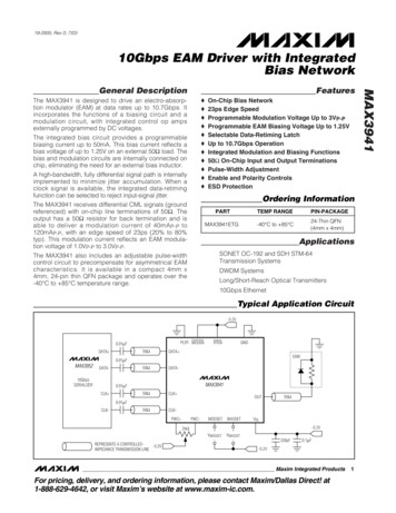
19-2935; Rev 0; 7/0310Gbps EAM Driver with IntegratedBias NetworkFeatures On-Chip Bias Network23ps Edge SpeedProgrammable Modulation Voltage Up to 3VP-PProgrammable EAM Biasing Voltage Up to 1.25VSelectable Data-Retiming LatchUp to 10.7Gbps OperationIntegrated Modulation and Biasing Functions50Ω On-Chip Input and Output TerminationsPulse-Width AdjustmentEnable and Polarity ControlsESD ProtectionOrdering InformationPARTTEMP RANGEPIN-PACKAGEMAX3941ETG-40 C to 85 C24-Thin QFN(4mm x 4mm)ApplicationsSONET OC-192 and SDH STM-64Transmission SystemsDWDM SystemsLong/Short-Reach Optical Transmitters10Gbps EthernetTypical Application Circuit-5.2VPLRT MODEN0.01µF50ΩDATA RTENGNDDATA ΩCLK 50ΩCLK-MAX39410.01µFCLK OUT50Ω0.01µFCLK-PWC PWC2kΩREPRESENTS A CONTROLLED-5.2VIMPEDANCE TRANSMISSION LINE.MODSETBIASSET VMODSET- VBIASSET-VEE-5.2V330pF0.1µF-5.2VMaxim Integrated ProductsFor pricing, delivery, and ordering information, please contact Maxim/Dallas Direct! at1-888-629-4642, or visit Maxim’s website at www.maxim-ic.com.1MAX3941General DescriptionThe MAX3941 is designed to drive an electro-absorption modulator (EAM) at data rates up to 10.7Gbps. Itincorporates the functions of a biasing circuit and amodulation circuit, with integrated control op ampsexternally programmed by DC voltages.The integrated bias circuit provides a programmablebiasing current up to 50mA. This bias current reflects abias voltage of up to 1.25V on an external 50Ω load. Thebias and modulation circuits are internally connected onchip, eliminating the need for an external bias inductor.A high-bandwidth, fully differential signal path is internallyimplemented to minimize jitter accumulation. When aclock signal is available, the integrated data-retimingfunction can be selected to reject input-signal jitter.The MAX3941 receives differential CML signals (groundreferenced) with on-chip line terminations of 50Ω. Theoutput has a 50Ω resistor for back termination and isable to deliver a modulation current of 40mA P-P to120mAP-P, with an edge speed of 23ps (20% to 80%typ). This modulation current reflects an EAM modulation voltage of 1.0VP-P to 3.0VP-P.The MAX3941 also includes an adjustable pulse-widthcontrol circuit to precompensate for asymmetrical EAMcharacteristics. It is available in a compact 4mm x4mm, 24-pin thin QFN package and operates over the-40 C to 85 C temperature range.
MAX394110Gbps EAM Driver with IntegratedBias NetworkABSOLUTE MAXIMUM RATINGSSupply Voltage VEE .-6.0V to 0.5VVoltage at MODEN,RTEN, PLRT, MODSET, BIASSET .(VEE - 0.5V) to 0.5VVoltage at DATA , DATA-, CLK , and CLK- -1.65V to 0.5VVoltage at OUT . .-4V to 0.5VVoltage at PWC , PWC- .(VEE - 0.5V) to (VEE 1.7V)Current Into or Out of OUT. .80mAContinuous Power Dissipation (TA 85 C)24-Lead Thin QFN(derate 20.8mW/ C above 85 C) .1354mWStorage Temperature Range . -55 C to 150 COperating Temperature Range . -40 C to 85 CLead Temperature (soldering, 10s) . 300 CStresses beyond those listed under “Absolute Maximum Ratings” may cause permanent damage to the device. These are stress ratings only, and functionaloperation of the device at these or any other conditions beyond those indicated in the operational sections of the specifications is not implied. Exposure toabsolute maximum rating conditions for extended periods may affect device reliability.ELECTRICAL CHARACTERISTICS(VEE -5.5V to -4.9V, TA -40 C to 85 C. Typical values are at VEE -5.2V, IBIAS 30mA, IMOD 100mA, and TA 25 C, unlessotherwise noted.)PARAMETERPower-Supply VoltageSupply CurrentPower-Supply Noise ding IBIAS andIMOD (Note 1)MAXUNITS-4.9VRetime disabled124174Retime enabled140201f 2MHz (Note 2)mA15dB10.7GbpsSIGNAL INPUT (Note 3)Input Data RatesSingle-Ended Input ResistanceNRZRINSingle-Ended Input VoltageVISDifferential Input VoltageVIDDifferential Input Return LossRLINInput to GND42.55058.5DC-coupled, Figure 1a-10AC-coupled, Figure 1b-0.4 0.4DC-coupled (Note 4)0.22.0AC-coupled (Note 4)0.21.6 15GHz15ΩVVP-PdBEAM BIASMaximum Bias CurrentVBIASSET VEE 2VMinimum Bias CurrentVBIASSET VEEBIASSET Voltage RangeVBIASSETEquivalent Bias ResistanceRBSEQVBias-Current-Setting AccuracyVEE(Note 6)mA1.2VEE 2VBIASSET VEE 0.11V2.14.3VBIASSET VEE 0.36V8.811.3VBIASSET VEE 2.0V5258.4VBIASSET VEE 0.36V-1100 1100VBIASSET VEE 0.36V-480 48050Ω driver load, VBIASSET VEE 0.55V,Figure 2mAVΩ36.4BIASSET Input ResistanceBIASSET Bandwidth560.3(Note 5)TA 25 CBias-Current TemperatureStability50mAppm/ C20kΩ5MHzEAM MODULATIONMaximum Modulation Current112Minimum Modulation CurrentVMODSET VEEMODSET Voltage RangeVMODSETEquivalent Modulation ResistanceRMODEQV212037VEE(Note 7)mAP-P40VEE 111.1mAP-PVΩ
10Gbps EAM Driver with IntegratedBias Network(VEE -5.5V to -4.9V, TA -40 C to 85 C. Typical values are at VEE -5.2V, IBIAS 30mA, IMOD 100mA, and TA 25 C, unlessotherwise noted.)PARAMETERSYMBOLCONDITIONSMINModulation depth 10%, 50Ω driver load,Figure 2Modulation Set BandwidthMODSET Input ResistanceModulation-Current TemperatureStability(Note 6)Modulation-Current-Setting ErrorOutput ResistanceROUTTYP-10OUT to GND42.5MHz20kΩ50BIASSET VEE, MODEN VEE, MODSET VEE, DATA high, DATA- lowTotal Off CurrentOutput Return LossRLOUTIBIAS 30mA,IMOD 50mAtSU, tHDFigure 3 (Note 6)Output Edge SpeedSetup/Hold Time(Notes 6, 8)Pulse-Width Control Input Range(Single Ended)For PWC and PWC-Pulse-Width Control Input Range(Differential)(PWC ) - (PWC-)δ0ppm/ C 10%58.5Ω1.2mA1020% to 80% (Notes 6, 8)Pulse-Width Adjustment RangeOutput Overshoot 15GHz23dB3225 30UNITS5-95750Ω driver load, TA 25 CMAXpsps 50psVEE 0.5VEE 1.5V-0.5 0.5V(Notes 6, 8)10%Driver Random JitterRJDR(Note 6)0.30.7psRMSDriver Deterministic JitterDJDRPWC- GND (Notes 6, 9)6.811psP-PCONTROL INPUTSInput High VoltageVIH(Note 10)Input Low VoltageVIL(Note 10)Input Current(Note 10)VEE 2.0-80VVEE 0.8V 200µANote 1: Supply current remains elevated once the retiming function is enabled. Power must be cycled to reduce supplycurrent after the retiming function is disabled.Note 2: Power-supply noise rejection is specified as PSNR 20log(Vnoise (on Vcc) / VOUT). VOUT is the voltage across a 50Ω load.Vnoise (on Vcc) 100mVP-P.Note 3: For DATA , DATA-, CLK , and CLK-.Note 4: CLK input characterized at 10.7Gbps.Note 5: RBSEQV (VBIASSET - VEE) / IBIAS with MODEN VEE, DATA high, and DATA- low.Note 6: Guaranteed by design and characterization using the circuit shown in Figure 4.Note 7: RMODEQV (VMODSET - VEE) / (IMOD - 37mA) with BIASSET VEE.Note 8: 50Ω load, characterized at 10.7Gbps with a 1111 1111 0000 0000 pattern.Note 9: Deterministic jitter is defined as the arithmetic sum of pulse-width distortion (PWD) and pattern-dependent jitter (PDJ).Measured with a 10.7Gbps 27 - 1 PRBS pattern with eighty 0s and eighty 1s inserted in the data pattern.Note 10: For MODEN and PLRT.3MAX3941ELECTRICAL CHARACTERISTICS (continued)
10Gbps EAM Driver with IntegratedBias NetworkMAX3941Test Circuits and Timing Diagrams0V100mV1.0V-0.5V-1.0V(a) DC-COUPLED SINGLE-ENDED CML INPUT0.4V800mV0V-0.4V100mV(b) AC-COUPLED SINGLE-ENDED (CML OR PECL) INPUTFigure 1. Definition of Single-Ended Input Voltage Range0V0VVOUTVOUTVBIASSET(a) MODULATING BIASSET(c) RESULT OF MODULATING BIASSETAND MODSET 180 OUT OF PHASE0VVOUTmWVMODSET(b) MODULATING MODSETPOUT(d) RESULTING OPTICAL OUTPUTNOTE: ALL AMPLITUDES ARE RELATIVE.Figure 2. Modulating BIASSET and MODSET Pins4
10Gbps EAM Driver with IntegratedBias NetworkCLK CLK-tSUVIS 0.1VP-P TO 1VP-PDC-COUPLED0.1VP-P TO 0.8VP-PAC-COUPLEDtHDDATA-VISDATA (DATA ) (DATA-)VID 0.2VP-P TO 2VP-PDC-COUPLED0.2VP-P TO 1.6VP-PAC-COUPLEDIOUTIMOD 40mAP-P TO 120mAP-PIBIAS 0mA TO 50mANOTE: IOUT RELATES TO RETIMED DATA.Figure 3. Setup and Hold Timing DefinitionGNDRTEN PWC 50Ω50ΩCLKD Q50Ω1DATA-VEE-5.2V0.1µF0DATA 50Ω300pF50ΩPWCCLK ure 4. AC-Characterization Circuit5MAX3941Test Circuits and Timing Diagrams (continued)
10Gbps EAM Driver with IntegratedBias NetworkMAX3941Test Circuits and Timing Diagrams (continued)VOLTAGEGNDVBIASVMODVOUTUSABLE RANGEVEE 1.9VBELOW USABLE RANGEFigure 5. Bias and Modulation Relationship to EAM VoltageTypical Operating Characteristics(Typical values are at VEE -5.2V, IBIAS 30mA, IMOD 100mA, TA 25 C, unless otherwise noted.)MAX3941 toc02MAX3941 toc01NOTE: BIAS AND MODULATION1 SET AT OPTIMUM LEVELS FOR EAM.2315ps/div20ps/div20ps/divPULSE WIDTH vs. RPWCRPWC- (Ω)2000 1750 1500 1250 1000 750 500 250160150IEE (mA)RETIMING ENABLED140130120RETIMING DISABLED110MEASURED AT 1.25GbpsWITH A 1010 PATTERN8408300820810800790780770760100750-40 -30 -20 -10 0 10 20 30 40 50 60 70 80 90TEMPERATURE ( C)6850PULSE-WIDTH POSITIVE PULSE (ps)MAX3941 toc04170MAX3941 toc05SUPPLY CURRENT vs. TEMPERATURE(50Ω LOAD, EXCLUDES IBIAS, IMOD)0250 500 750 1000 1250 1500 1750 2000RPWC (Ω)MAX3941 toc03OC-192 OPTICAL EYE DIAGRAM(OC-192 FILTER, 231 - 1 PRBS)10Gbps ELECTRICAL EYE DIAGRAM(VMOD 3VP-P, 231 - 1 PRBS)10Gbps ELECTRICAL EYE DIAGRAM(VMOD 1VP-P, 231 - 1 PRBS)
10Gbps EAM Driver with IntegratedBias NetworkPULSE-WIDTH DISTORTIONvs. TEMPERATUREVMOD vs. VMODSET(ZL 50Ω)4.0MAX3941 toc074.5VMODSET IS RELATIVE TO VEE.3.02.53.5VMOD 050709000.250.500.75TEMPERATURE ( C)VMODSET (V)VBIAS vs. VBIASSET(ZL 50Ω)POWER-SUPPLY NOISE REJECTIONvs. FREQUENCY30MAX3941 toc080VBIASSET IS RELATIVE TO VEE-0.21.00MAX3941 toc09PULSE-WIDTH DISTORTION (ps)3.5MAX3941 toc065.02520-0.6PSNR (dB)VBIAS 0010FREQUENCY (Hz)DIFFERENTIAL S11 vs. FREQUENCY(DEVICE POWERED)S22 vs. FREQUENCY(DEVICE POWERED)0MAX3941 toc100-510k1kVBIASSET (V)MAX3941 toc110-4-8-10-15 S22 (dB) S11 QUENCY (GHz)121503691215FREQUENCY (GHz)7MAX3941Typical Operating Characteristics (continued)(Typical values are at VEE -5.2V, IBIAS 30mA, IMOD 100mA, TA 25 C, unless otherwise noted.)
10Gbps EAM Driver with IntegratedBias NetworkMAX3941Pin DescriptionPINNAMEFUNCTION1DATA Noninverting Data Input with 50Ω On-Chip Termination2DATA-Inverting Data Input with 50Ω On-Chip Termination3, 4, 14GNDGround. All pins must be connected to board ground.5CLK Noninverting Clock Input for Data Retiming with 50Ω On-Chip Termination6CLK-Inverting Clock Input for Data Retiming with 50Ω On-Chip Termination7, 11, 12, 13,18, 19, 24VEE8PWC Positive Input for Modulation Pulse-Width Adjustment (See the Design Procedure Section)9PWC-Negative Input for Modulation Pulse-Width Adjustment. Ground to disable the pulse-widthadjustment feature (see the Design Procedure section).10MODSETModulation Current Set. Apply a voltage to set the modulation current of the driver output.15GND116OUT17GND2Ground. Ground connection.20PLRTDifferential Data Polarity Swap Input. Set high or float for normal operation. Set low to invert thedifferential signal polarity. Contains an internal 100kΩ pullup to GND.21BIASSETBias Current Set. Apply a voltage to set the bias current of the driver output.22MODENTTL/CMOS Modulation Enable Input. Set low or float for normal operation. Set high to put the EAMin the absorption (logic 0) state. Contains an internal 100kΩ pulldown to VEE.23RTENData-Retiming Input. Connect to VEE for retimed data. Connect to GND to bypass retiming latch.EPExposedPadNegative Supply Voltage. All pins must be connected to board VEE.Ground. Ground connection.Driver Output. Provides both modulation and bias output. DC-couple to EAM.Ground. Must be soldered to the circuit board ground for proper thermal and electrical performance(see the Exposed Pad Package section).Detailed DescriptionThe MAX3941 EAM driver consists of two main parts: ahigh-speed modulation driver and an EAM-biasingblock. The clock and data inputs to the driver are compatible with PECL and CML logic levels. The modulation and bias currents are output through the OUT pin.The modulation output stage is composed of a highspeed differential pair and a programmable currentsource with a maximum modulation current of 120mA.The rise and fall times are typically 23ps. The modulationcurrent is designed to produce an EAM voltage up to3.0VP-P when driving a 50Ω module. The 3.0VP-P resultsfrom 120mAP-P through the parallel combination of the50Ω EAM load and the internal 50Ω back termination.8Polarity SwitchThe MAX3941 includes a polarity switch. When thePLRT pin is high or left floating, the output maintains thepolarity of the input data. When the PLRT pin is low, theoutput is inverted relative to the input data.Clock/Data Input Logic LevelsThe MAX3941 is directly compatible with ground-reference CML. Either DC- or AC-coupling can be used forCML referenced to ground. For all other logic types,AC-coupling should be used.Optional Data Input LatchTo reject pattern-dependent jitter in the input data, a synchronous differential clock signal should be connected tothe CLK and CLK- inputs, and the RTEN control inputshould be connected to VEE.
10Gbps EAM Driver with IntegratedBias Network(ZL) in parallel with the internal 50Ω termination resistor(ROUT):Pulse-Width ControlTo program the desired bias current, force a voltage atthe BIASSET pin (see the Typical Application Circuit).The resulting IBIAS current can be calculated by the following equation:The pulse-width control circuit can be used to compensate for pulse-width distortion introduced by the EAM.The differential voltage between PWC and PWCadjusts the pulse-width compensation. The adjustmentrange is typically 50ps. Optional single-ended operation is possible by forcing a voltage on the PWC pinwhile leaving the PWC- pin unconnected. When PWCis connected to ground, the pulse-width control circuitis automatically disabled.Modulation Output EnableThe MAX3941 incorporates a modulation currentenable input. When MODEN is low or floating, the modulation/bias output (OUT) is enabled. When MODEN ishigh, the output is switched to the logic 0 state. Thetypical enable time is 2ns and the typical disable timeis 2ns.Design ProcedureProgramming the Modulation VoltageThe EAM modulation voltage results from IMOD passingthrough the EAM impedance (ZL) in parallel with theinternal 50Ω termination resistor (ROUT):VMOD IMOD ZL ROUTZL ROUTTo program the desired modulation current, force avoltage at the MODSET pin (see the Typical ApplicationCircuit). The resulting IMOD current can be calculatedby the following equation:IMOD VMODSET 37mA11.1ΩAn internal, independent current source drives a constant37mA to the modulation circuitry, and any voltage aboveVEE on the MODSET pin adds to this. The input impedance of the MODSET pin is typically 20kΩ. Note that theminimum output voltage is VEE 1.9V (Figure 5).Programming the Bias VoltageAs in the case of modulation, the EAM bias voltageresults from IBIAS passing through the EAM impedanceVBIAS IBIAS ZL ROUTZL ROUTVBIASSET36.4ΩIBIAS The input impedance of the BIASSET pin is typically20kΩ. Note that the minimum output voltage is VEE 1.9V (Figure 5).Programming the Pulse-Width ControlThree methods of control are possible when pulse predistortion is desired to minimize distortion at the receiver.The pulse width can be set with a 2kΩ potentiometer withthe center tapped to VEE (or equivalent fixed resistors),by applying a voltage to the PWC pin, or by applying adifferential voltage across the PWC and PWC- pins. SeeTable 1 for the desired effect of the pulse-width setting.Pulse width is defined as (positive pulse width)/((positivepulse width negative pulse width)/2).Input Termination RequirementThe MAX3941 data and clock inputs are CML compatible. However, it is not necessary to drive the IC with astandard CML signal. As long as the specified input voltage swings are met, the MAX3941 operates properly.Applications InformationLayout ConsiderationsTo minimize loss and crosstalk, keep the connectionsbetween the MAX3941 output and the EAM module asshort as possible. Use good high-frequency layouttechniques and multilayer boards with an uninterruptedground plane to minimize EMI and crosstalk. Circuitboards should be made using low-loss dielectrics. Usecontrolled-impedance lines for the clock and datainputs as well as for the data output. Be sure to filter thepower supply with capacitors placed close to the IC.Table 1. Pulse-Width ControlRPWC RPWC-VPWC (PWC- OPEN)(V)VEE 1VPWC VPWC(V)0 100RPWC RPWC- VEE 1 0 100RPWC RPWC- VEE 1 0PULSEWIDTH(%)100RPWC , RPWC- FORRPWC RPWC- 2kΩ9MAX3941The input data is retimed on the rising edge of CLK . IfRTEN is connected to ground, the retiming function is disabled and the input data is directly connected to the output stage. Leave CLK and CLK- open when retiming isdisabled.
MAX394110Gbps EAM Driver with IntegratedBias 50Ω50Ω50ΩOUTCLK VEECLK-DQZL0POLARITYMUXPWCDATA 1IMODDATA50ΩIBIAS50ΩMAX3941VEEPWC PWC-2kΩVEEMODSETBIASSET VMODSET-VBIASSET-VEEVEEVEEFigure 6. Functional DiagramInterface SchematicsLaser Safety and IEC 825Figures 7 and 8 show simplified input and output circuits of the MAX3941 EAM driver.Using the MAX3941 EAM driver alone does not ensurethat a transmitter design is compliant with IEC 825. Theentire transmitter circuit and component selections mustbe considered. Each customer must determine the levelof fault tolerance required by their application, recognizing that Maxim products are not designed or authorizedfor use as components in systems intended for surgicalimplant into the body, for applications intended to support or sustain life, or for any other application where thefailure of a Maxim product could create a situation wherepersonal injury or death may occur.Exposed-Pad PackageThe exposed pad on the 24-pin QFN provides a very lowthermal-resistance path for heat removal from the IC. Thepad is also electrically ground on the MAX3941 and mustbe soldered to the circuit board for proper thermal andelectrical performance. Refer to Maxim Application NoteHFAN-08.1: Thermal Considerations for QFN and OtherExposed-Pad Packages for additional Information.10
10Gbps EAM Driver with IntegratedBias ATA /CLK GND50ΩGNDOUTDATA-/CLKVEEVEEFigure 8. Simplified Output CircuitFigure 7. Simplified Input CircuitPin 9TOP VIEWPackage InformationFor the latest package outline information, go to www.maximic.com/packages.PARTPACKAGE TYPEPACKAGE CODEMAX3941ETG24-Thin QFN4mm x 4mm x 0.8mmT2444-1DATA 118VEEDATA-217GND2GND316OUT15GND1TRANSISTOR COUNT: 1918PROCESS: SiGe 1485PWC CLK 74VEE.GNDChip InformationTHIN QFN (4mm x 4mm)EXPOSED PAD CONNECTED TO GROUNDMaxim cannot assume responsibility for use of any circuitry other than circuitry entirely embodied in a Maxim product. No circuit patent licenses areimplied. Maxim reserves the right to change the circuitry and specifications without notice at any time.Maxim Integrated Products, 120 San Gabriel Drive, Sunnyvale, CA 94086 408-737-7600 11 2003 Maxim Integrated ProductsPrinted USAis a registered trademark of Maxim Integrated Products.MAX3941GND
typ). This modulation current reflects an EAM modula-tion voltage of 1.0VP-P to 3.0VP-P. The MAX3941 also includes an adjustable pulse-width control circuit to precompensate for asymmetrical EAM characteristics. It is available in a compact 4mm x 4mm, 24-pin thin QFN package and operates over the -40 C to 85 C temperature range. Features