Transcription
NXP SemiconductorsUser's GuideDocument Number: MBOOTQSPIUGRev 2, 05/2018MCU Bootloader QuadSPI User's Guide
ContentsContentsChapter 1 Introduction.4Chapter 2 Overview.52.1 Terminology. 52.2 Requirements. 62.2.1 Hardware requirements.62.2.2 Host tools.62.2.3 Demo application. 62.2.4 Required toolchains. 62.2.4.1 Firmware project. 62.2.4.2 Host project.72.3 QuadSPI image boot procedure. 72.3.1 Plaintext QuadSPI image boot flow. 72.3.2 Encrypted QuadSPI image boot flow.7Chapter 3 Creating application for QuadSPI memory. 93.1 Starting point: Basics of internal flash memory mapped led-demo example project. 93.2 Changes to the led-demo project.103.2.1 Changes to the linker file.103.2.2 Changes to flash config area.113.2.3 Configure BCA. 113.3 Generate QCB. 133.3.1 The QCB structure. 133.3.2 Example QCB for MX25U3235F device on TWR-K80F150M Tower System module.213.3.3 Generate the QCB with a simple example project. 24Chapter 4 Configure QuadSPI with MCU bootloader.284.1 Configure QuadSPI at runtime.284.2 Configure QuadSPI at start-up. 29Chapter 5 Flash QuadSPI image via SB file.315.1 Brief introduction of SB file. 315.2 Generate SB file for QuadSPI image. 315.3 Flash QuadSPI image via MCU bootloader.33Chapter 6 Advanced Usage: Encrypted QuadSPI image.356.1 Generate an SB file with KEK and SB KEY.366.2 Generate an SB file with encrypted QuadSPI image.376.2.1 The KeyBlob Block.386.2.2 Encrypt QuadSPI image. 386.2.3 Encrypting SB file with the SB key.39Chapter 7 Change QuadSPI clock in QuadSPI image.417.1 Create a RAM function via IAR EWARM.41MCU Bootloader QuadSPI User's Guide, Revision 2, May 20182NXP Semiconductors
Contents7.2 Create a RAM function via Keil MDK.427.3 Create a RAM function with MCUXpresso IDE. 437.4 Ensure no timing issue after clock change. 45Chapter 8 Application running on QuadSPI alias area. 468.1 Create an application to run on QuadSPI Alias Area.468.2 Create a simple boot application. 488.3 Downloading application running on QuadSPI alias memory with SB file.518.4 Creating encrypted QuadSPI application running on QuadSPI Alias memory with SB file52Chapter 9 Appendix A - QuadSPI configuration procedure. 54Chapter 10 Appendix B - Re-enter MCU bootloader under direct bootmode. 55Chapter 11 Appendix C - Explore more features in QCB.5611.1 Parallel mode.5611.2 Continuous read mode. 58Chapter 12 Appendix D - DDR mode issue workaround.6012.1 Example QCB for QuadSPI device N25Q256A with DDR mode support. 6012.2 Example QCB for QuadSPI device S26KS128S with Octal DDR mode support. 6112.3 Changes to user application for implementing DDR mode path. 6312.3.1 Workaround solution. 6312.3.2 Changes to linker file. 6412.3.3 Changes to startup file. 6512.3.4 Changes to system MK82F25615.c file.6512.4 Workaround block diagram. 6712.5 BD file for downloading QuadSPI image under DDR mode.68Chapter 13 Revision history. 70MCU Bootloader QuadSPI User's Guide, Revision 2, May 2018NXP Semiconductors3
IntroductionChapter 1IntroductionThe QuadSPI controller available on selected Kinetis devices supports execute-in-place (XIP) for external SPI flash memorydevices. This document describes the usage of MCU bootloader (MCUBOOT) in configuring various features of QuadSPIblock, including XIP, generating plaintext and encrypted bootable SB file image, and flashing QuadSPI memory with the SBfile image.QuadSPI features supported by MCU bootloader: Various types of SPI NOR flash memory devices available in the market. Flash memory booting from QuadSPI directly, using MCU bootloader. Single/Dual/Quad and Octal SPI NOR flash memory devices. High-performance read/write operation with parallel and DDR modes. Protecting intellectual property with AES-128 algorithm.MCU Bootloader QuadSPI User's Guide, Revision 2, May 20184NXP Semiconductors
OverviewTerminologyChapter 2OverviewThis document mainly focuses on the following topics: QuadSPI image boot procedure Creating an application image running on QuadSPI memory Configuring QuadSPI with MCU bootloader Programming QuadSPI memory with SB file Advanced usage: QuadSPI encrypted boot image Application requirements for re-configuring QuadSPI clockIn addition, the following topics are also covered in the appendix sections: QuadSPI configuration block (QCB) Re-enter MCU bootloader under direct boot mode Explore features supported in QCB Working around ROM issues in supported DDR mode devices2.1 TerminologyThe following table summarizes the terms and abbreviations included in this user's guide.Table 1. Terminology and abbreviationsTerminologyDescriptionMCUBOOTBCAMCU bootloaderBootloader Configuration Area, which provides customization of bootloaderoptions, such as enabledPeripherals, peripheralDetectionTimeout, and so on.See the MCU bootloader chapter in the silicon's reference manual for more details.QCBQuadSPI Configuration Block, a structure containing configurable parametersneeded by the MCU bootloader to configure the QuadSPI controller.See the MCU bootloader chapter in the silicon's reference manual for more details.KeyBlobA data structure which holds the KeyBlob entries. Each keyblob entry defines theencrypted QuadSPI memory region, decryption key, and so on.See the MCU bootloader chapter in the silicon's reference manual for more details.KEKKeyBlob Encryption Key, an AES-128 key used for encrypting plaintext KeyBloband decrypting encrypted KeyBlob.See the MCU bootloader chapter in the silicon's reference manual for more details.Table continues on the next page.MCU Bootloader QuadSPI User's Guide, Revision 2, May 2018NXP Semiconductors5
OverviewRequirementsTable 1. Terminology and abbreviations (continued)TerminologyDescriptionSB fileThe SB file is the NXP binary file format for bootable images. The file consists ofsections and sequence of bootloader commands and data that assists MCUbootloader in programming the image to target memory. The image data in theSB file can be encrypted as well. The file can be downloaded to the target usingthe MCU bootloader receive-sb-file command.See the MCU bootloader chapter in silicon's reference manual for more detailsOTFADOn-the-fly AES Decryption is a powerful IP block in MK81F256 and MK82F256,which supports decryption of the encrypted QuadSPI image on-the-fly usingKeyBlob.See the MCU bootloader chapter in the silicon's reference manual for more details2.2 Requirements2.2.1 Hardware requirements TWR-K80F150M Tower System module FRDM-K82F Freedom Development platform TWR-KL82 Tower System module FRDM-KL82 Freedom Development platform2.2.2 Host toolsThe following host tools are available with the release package. They assist in generating and provisioning of QuadSPIbootable image for the target device. blhost: command line host tool for MCU bootloader. elftosb: command line host tool for SB file generation. KinetisFlashTool: GUI host tool for MCU bootloader.2.2.3 Demo applicationLed demo running in internal flash and QuadSPI memory, under sdk package /boards/ board /bootloader examples/demo appsQCBGenerator, under sdk package /middleware/mcu-boot/apps/QCBGenerator/build2.2.4 Required toolchains2.2.4.1 Firmware projectThe following toolchains can be used to build the example led demo firmware application provided with the release package. ARM Keil development tool v5.24a with corresponding device pack IAR Embedded Workbench for ARM v8.20.2MCU Bootloader QuadSPI User's Guide, Revision 2, May 20186NXP Semiconductors
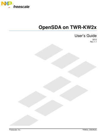
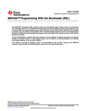
OverviewQuadSPI image boot procedure MCUXpresso IDE v10.1.12.2.4.2 Host projectThe following toolchains can be used to build the example QCBGenerator application provided with the release package. Microsoft Visual Studio Professional 2015 for Windows OS Desktop Codeblocks GCC v5.4.02.3 QuadSPI image boot procedureTo understand how to boot a QuadSPI image with MCU bootloader, it is necessary to understand the QuadSPI image bootflow. There are two types of QuadSPI image boot flow: Boot from a plaintext QuadSPI image. This method can be used on all targets with QuadSPI support. Boot from an encrypted QuadSPI image. This method can only be used on K8x processors that include OTFAD support,such as MK81F256 and MK82F256.2.3.1 Plaintext QuadSPI image boot flowThe figure below shows the boot flow of MCU bootloader in booting the device with a plaintext QuadSPI image.Figure 1. Plaintext QuadSPI image boot flow2.3.2 Encrypted QuadSPI image boot flowThe below figure shows the boot flow of MCU bootloader in booting the device with an encrypted QuadSPI image.MCU Bootloader QuadSPI User's Guide, Revision 2, May 2018NXP Semiconductors7
OverviewQuadSPI image boot procedureFigure 2. Encrypted QuadSPI image boot flowMCU Bootloader QuadSPI User's Guide, Revision 2, May 20188NXP Semiconductors
Creating application for QuadSPI memoryStarting point: Basics of internal flash memory mapped led-demo example projectChapter 3Creating application for QuadSPI memoryThis section describes how to modify a normal flash application (led demo) to run from QuadSPI. The fully functional LEDdemo example for QuadSPI with source code can be found in sdk package /boards/ board /bootloader examples/demo apps. The chapter also discuss on how to create QCB data structure for a typical QuadSPI flash memory device.3.1 Starting point: Basics of internal flash memory mappedled-demo example projectStart from the LED demo example project code for the MK82F256 device. The example led-demo project files for each of thesupported toolchains are available in sdk package /boards/ board /bootloader examples/demo apps folder of thepackage. This document focuses on the IAR project examples only. Open the led demo.eww file from the IAR folder andselect the led demo PFLASH project as the active project. See the following figure.Note that the linker file for the led demo PFLASH project shows all sections located in the internal flash memory region,including the vector table, flash config area, and text sections.When the led demo PFLASH image is built and flashed to the internal flash memory of the target device and begins itsexecution, it causes the blue and green LEDs to blink on the target board.The subsequent sections show the changes needed to convert the led demo PLASH project to run on the QuadSPI memoryfor the target device.MCU Bootloader QuadSPI User's Guide, Revision 2, May 2018NXP Semiconductors9
Creating application for QuadSPI memoryChanges to the led-demo projectFigure 3. The led demo PFLASH project3.2 Changes to the led-demo projectThe following subsections describe the steps to map the led-demo to run from the external QuadSPI flash memory.3.2.1 Changes to the linker fileThe first step is to update the linker file. The m text start, and m text end symbol names must be updated. The addressof m text start should be changed to 0x68001000, and m text end to 0x6FFFFFFF or the actual end address of theselected SPI flash device. See the changes in the following figure.MCU Bootloader QuadSPI User's Guide, Revision 2, May 201810NXP Semiconductors
Creating application for QuadSPI memoryChanges to the led-demo projectFigure 4. Linker file changes3.2.2 Changes to flash config areaThe bit 7-6 in the FOPT (0x40D) must be changed to 0b’10 to select the ROM as the boot source upon reset. The QuadSPIis configured after the ROM starts and when the QCB is present. After this operation, the flash config area is changed, asshown in the following figure.Figure 5. Change flash config area for QuadSPI imageSee the startup MK82F2515 qspi.s file in the led demo- sdk package /middleware/mcu-boot/apps/demo qspi/led demo/devices/MK80F25615/startup/ toolchain folder for more details.3.2.3 Configure BCAAfter the previous step, the target is able to run the led-demo application once the active peripheral detection timeout occurs.To customize the boot option for the QuadSPI image, the BCA is required. The first step to is to defineBOOTLOADER CONFIG in the project. Implement the operation shown in the following figure for IAR EWARM toolchain asan example.MCU Bootloader QuadSPI User's Guide, Revision 2, May 2018NXP Semiconductors11
Creating application for QuadSPI memoryChanges to the led-demo projectFigure 6. Enable BCA in EWARMThere are two ways to configure the QuadSPI image boot option:1. Change the peripheralDetectionTimeoutMs. For example, change it to 0x01F4 (500 ms).2. Change the bootFlags to 0xFE, which means boot directly from application without delay. To re-enter MCU bootloaderagain, see Appendix B.NOTEThe first way to configure the QuadSPI image boot option is recommended.In this example, there is a BootloaderConfig constant variable defined in system MK82F25615.c. It can be changed as shownin the following figure.When the BCA change is complete, the target supports execution of led demo image if it has been programmed to internalflash or QuadSPI memory.MCU Bootloader QuadSPI User's Guide, Revision 2, May 201812NXP Semiconductors
Creating application for QuadSPI memoryGenerate QCBFigure 7. Set peripheralDetectionTimeoutMs to 500 ms3.3 Generate QCBQuadSPI Config Block (QCB) is required for MCU ROM bootloader to properly configure and access the QuadSPI device.This section shows the QCB structure, determines the QCB parameters for the specified SPI flash device, and generatesthe QCB with a simple project.3.3.1 The QCB structureThe QCB is a data structure containing the most common used parameters for QuadSPI module. See the MCU bootloaderchapter in the silicon’s reference manual for more details. The QCB is organized as follows.MCU Bootloader QuadSPI User's Guide, Revision 2, May 2018NXP Semiconductors13
Creating application for QuadSPI memoryGenerate QCBTable 2. QuadSPI configuration blockOffsetSize (bytes)Configuration fieldDescription0x00 - 0x034tagMagic number to verify whether QCB is valid.Must be set to ‘kqcf’.[31:24] - ‘f’ (0x66)[23:16] - ‘c’ (0x63)[15: 8] - ‘q’(0x71)[7: 0] - ‘k’(0x6B)0x04 - 0x074versionVersion number of QuadSPI config block.[31:24] - name: must be ‘Q’(0x51)[23:16] - major: must be 1[15: 8] - minor: must be 1[7: 0] - bugfix: must be 00x08 - 0x0b4lengthInBytesSize of QuadSPI config block, in terms ofbytes.Must be 512.0x0c - 0x0f4dqs loopbackEnable DQS loopback support:0 DQS loopback is disabled.1 DQS loopback is enabledd, the DQS loopbackmode is determined by subsequent'dqs loopback internal' field.0x10 - 0x134data hold timeSerial flash data hold time. Valid value 0/1/2.See the QuadSPI Chapter for details.0x14 - 0x1b8-Reserved.0x1c - 0x1f4device mode configenConfigure work mode enable for external flashdevices:0 Disabled - ROM does not configure work modeof external flash devices.1 Enabled - ROM configures work mode ofexternal flash devices based on "device cmd"and LUT entries indicated by "write cmd ipcr".0x20 - 0x234device cmdCommand to configure work mode of externalflash devices. Effective only if"device mode config en" is set to 1.This command is device-specific.Table continues on the next page.MCU Bootloader QuadSPI User's Guide, Revision 2, May 201814NXP Semiconductors
Creating application for QuadSPI memoryGenerate QCBTable 2. QuadSPI configuration block (continued)OffsetSize (bytes)Configuration fieldDescription0x24 - 0x274write cmd ipcrIPCR pointed to LUT index for the commandsequence of configuring the device to workmode.Value index 240x28 - 0x2b4word addressableWord addressable:0 Byte addressable serial flash mode.1 Word addressable serial flash mode.0x2c - 0x2f4cs hold timeSerial flash CS hold time in terms of flash clockcycles.0x30 - 0x334cs setup timeSerial flash CS setup time in terms of flashclock cycles.0x34 - 0x374sflash A1 sizeSize of external flash connected to ports ofQSPI0A and QSPI0A CS0, in terms of bytes.0x38 - 0x3b4sflash A2 sizeSize of external flash connected to ports ofQSPI0B and quadSPI0A CS1, in terms ofbytes.This field must be set to 0 if the serial flashdevices are not present.0x3c - 0x3f4sflash B1 sizeSize of external flash connected to ports ofQSPI0B and quadSPI0B CS0, in terms ofbytes.This field must be set to 0 if the serial flashdevices are not present.0x40 - 0x434sflash B2 sizeSize of external flash connected to ports ofQSPI0B and quadSPI0B CS1, in terms ofbytes.This field must be set to 0 if the serial flashdevices are not present.0x44 - 0x474sclk freqFrequency of QuadSPI serial clock:0 Low frequency1 Mid frequency2 High frequencySee the MCU bootloader chapter in silicon’sreference manual for the definition of lowfrequency, mid-frequency and high-frequency. InMK82F256, they are 24 MHz, 48 MHz, and 96MHz.Table continues on the next page.MCU Bootloader QuadSPI User's Guide, Revision 2, May 2018NXP Semiconductors15
Creating application for QuadSPI memoryGenerate QCBTable 2. QuadSPI configuration block (continued)OffsetSize (bytes)Configuration fieldDescription0x48 - 0x4b4busy bit offsetBusy bit offset in status register of Serial flash[31:16]:0 - Busy flag in status register is 1 when flashdevices are busy.1 - Busy flag in status register is 0 when flashdevices are busy.[15:0]:The offset of busy flag in status register, validrange 0-31.0x4c - 0x4f4sflash typeType of serial flash:0 Single-pad1 Dual-pad2 Quad-pad3 Octal-pad0x50 - 0x534sflash portPort enablement for QuadSPI module:0 Only pins for QSPI0A are enabled.1 Pins for both QSPI0A and QSPI0B areenabled.0x54 - 0x574ddr mode enableEnable DDR mode:0 DDR mode is disabled.1 DDR mode is enabled.0x58 - 0x5b4dqs enableEnable DQS:0 DQS is disabled.1 DQS is enabled.0x5c - 0x5f4parallel mode enable Enable Parallel Mode:0 Parallel mode is disabled.1 Parallel mode is enabled.0x60 - 0x634portA cs1Enable QuadSPI0A CS1:0 QuadSPI0A CS1 is disabled.1 QuadSPI0A CS1 is enabled.This field must be set to 1 if sflash A2 size isnot equal to 0.Table continues on the next page.MCU Bootloader QuadSPI User's Guide, Revision 2, May 201816NXP Semiconductors
Creating application for QuadSPI memoryGenerate QCBTable 2. QuadSPI configuration block (continued)OffsetSize (bytes)Configuration fieldDescription0x64 - 0x674portB cs1Enable QuadSPI0B CS10 QuadSPI0B CS1 is disabled1 QuadSPI0B CS1 is enabledThis field must be set to 1 if sflash B2 size isnot equal to 0.0x68 - 0x6b4fsphsFull Speed Phase selection for SDRinstructions:0 Select sampling at non-inverted clock.1 Select sampling inverted clock.0x6c - 0x6f4fsdlyFull Speed Delay selection for SDRinstructions:0 One clock cycle delay.1 Two clock cycles delay.0x70 - 0x734ddrsmpDDR sampling point:Valid range: 0 - 7.0x74 - 0x173256look up tableLook-up-table for sequences of instructions.See the QuadSPI chapter in silicon’s referencemanual for more details.0x174 - 0x1774column address spac Column Address Space:eThe parameter defines the width of the columnaddress.0x178 - 0x17b4config cmd enEnable additional configuration command:0 Additional configuration command is notneeded.1 Additional configuration command is needed.0x17c - 0x18b16config cmdsIPCR arrays for each connected SPI flash."config cmds[n]" provides IPCR value, namelyseq id 24.All fields must be set to 0 if config cmd en is notset.Table continues on the next page.MCU Bootloader QuadSPI User's Guide, Revision 2, May 2018NXP Semiconductors17
Creating application for QuadSPI memoryGenerate QCBTable 2. QuadSPI configuration block (continued)OffsetSize (bytes)Configuration fieldDescription0x18c - 0x19b16config cmds argsCommand arrays needed to be transferred toexternal SPI flash."config cmds args[n]" provides commands tobe written.All fields must be set to 0 if config cmd en is notasserted.0x19c - 0x19f4differential clock pinenableEnable differential flash clock pin:0 Differential flash clock pin is disabled.1 Differential flash clock pin is enabled.0x1a0 - 0x1a34flash CK2 clock pin Enable flash CK2 clock pin:enable0 Flash CK2 clock pin is disabled.1 Flash CK2 clock pin is enabled.0x1a4 - 0x1a74dqs inverse selSelect clock source for internal DQSgeneration:0 Use 1x internal reference clock for DQSgeneration.1 Use inverse 1x internal reference clock for theDQS generation.0x1a8 - 0x1ab4dqs latency enableDQS Latency Enable:0 DQS latency disabled.1 DQS feature with latency included enabled.0x1ac - 0x1af4dqs loopback internal DQS loop back from internal DQS signal orDQS Pad:0 DQS loop back is sent to DQS pad first andthen looped back to QuadSPI.1 DQS loop back from internal DQS signaldirectly.0x1b0 - 0x1b34dqs phase selSelect Phase Shift for internal DQSgeneration:0 No Phase shift.1 Select 45 degree phase shift.2 Select 90 degree phase shift.3 Select 135 degree phase shift.0x1b4 - 0x1b74dqs fa delay chain s Delay chain tap number selection forelQuadSPI0A DQS:Valid range: 0-63Table continues on the next page.MCU Bootloader QuadSPI User's Guide, Revision 2, May 201818NXP Semiconductors
Creating application for QuadSPI memoryGenerate QCBTable 2. QuadSPI configuration block (continued)OffsetSize (bytes)Configuration fieldDescription0x1b8 - 0x1bb4dqs fb delay chain s Delay chain tap number selection forelQuadSPI0B DQS:Valid range: 0-630x1bc - 0x1c38-Reserved.0x1c4 - 0x1c74page sizePage size of external flash.Page size of all SPI flash devices must be thesame.0x1c8 - 0x1cb4sector sizeSector size of exernal SPI in flash.Sector size of all SPI flash devices must be thesame.0x1cc - 0x1cf4timeout millisecondsTimeout in terms of milliseconds:0 Timeout check is disabled.Other: QuadSPI Driver returns timeout if thetime that external SPI devices are busy lastsmore than this value.0x1d0 - 0x1d34ips cmd second dividerSecond driver for IPs command based onQSPI MCR[SCLKCFG], the maximum value ofQSPI MCR[SCLKCFG] depends on specificdevices.0x1d4 - 0x1d74need multi phase0 Only one phase is needed to access externalflash devices.1 Multiple phases are needed to erase/programexternal flash devices.0x1d8 - 0x1db4is spansion hyperflas 0 External flash devices do not belong tohCypress HyperFlash family.1 External flash devices belong to CypressHyperFlash family.0x1dc - 0x1df4pre read status cmdaddress offsetAdditional address for the PreReadStatuscommand.Set this field to 0xFFFFFFFF if it is not required.0x1e0 - 0x1e34pre unlock cmd addr Additional address for PreWriteEnableess offsetcommand.Set this field to 0xFFFFFFFF if it is not required.0x1e4 - 0x1e74unlock cmd address Additional address for WriteEnable command.offsetSet this field to 0xFFFFFFFFF if it is notrequired.Table continues on the next page.MCU Bootloader QuadSPI User's Guide, Revision 2, May 2018NXP Semiconductors19
Creating application for QuadSPI memoryGenerate QCBTable 2. QuadSPI configuration block (continued)OffsetSize (bytes)Configuration fieldDescription0x1e8 - 0x1eb4pre program cmd address offsetAddtional address for PrePageProgramcommand.Set this field to 0xFFFFFFFF if it is not required.0x1ec - 0x1ef4pre erase cmd addre Additional address for PreErase command.ss offsetSet this field to 0xFFFFFFFF if it is not required.0x1f0 - 0x1f34erase all cmd address offsetAdditional address for EraseAll command.-Reserved.0x1f4 - 0x1ff12Set this field to 0xFFFFFFFF if it is not required.NOTE1. Though there are several parameters in QCB, only a few parameters need to be configured formost SPI flash devices available on the market. See the example QCB for more details.2. While using MCU ROM bootloader, make sure the "ips cmd second divider" is not greaterthan 0x08 under SDR mode, and it is not greater than 2 under DDR mode.3. It is recommended to configure QSPI to SDR mode and switch to DDR mode in the applicationwhere possible to achieve higher program performance with MCU bootloader.In the QCB, the most important field is the Lookup Table (LUT), which contains command sequence for QuadSPI instructions,such as erase, read, and program. The command sequence in the LUT should appear in the order as shown in the followingtable:Table 3. Look-up table entries for MCU bootloaderIndexFieldDescription0ReadSequence for read instructions.1WriteEnableSequence for WriteEnable instructions.2EraseAllSequence for EraseAll instructions, optional.3ReadStatusSequence for ReadStatus instructions.4PageProgramSequence for Page Program instructions.6PreEraseSequence for Pre-Erase instructions.7SectorEraseSequence for Sector Erase.8DummySequence for dummy operation if neededFor example, if continuous read is configured inindex 0, the dummy LUT should be configured toforce external SPI flash to exit continuous readmode. If it is not required, this LUT entry must beset to 0.9PreWriteEnableSequence for Pre-WriteEnable instructions.Table continues on the next page.MCU Bootloader QuadSPI User's Guide, Revision 2, May 201820NXP Semiconductors
Creating application for QuadSPI memoryGenerate QCBTable 3. Look-up table entries for MCU bootloader quence for Pre-PageProgram instructions.11PreReadStatusSequence for Pre-ReadStatus instructions.5, 12, 13, 14, 15UndefinedAll of these sequences are free to be used for otherpurposes. I.e., index 5 can be used for enablingQuad mode of SPI flash devices. For more details,see Section 3.3.2, "Example QCB forMX25U3235F device on TWR-K80F150M TowerSystem module".For most types of SPI, flash devices are available in the market. Only index 0, 1, 3, 4, 7, and 8 are required. However, forother types of high-end SPI flash devices, such as Cypress HyperFlash, additional indexes list
SB file The SB file is the NXP binary file format for bootable images. The file consists of sections and sequence of bootloader commands and data that assists MCU bootloader in programming the image to target memory. The image data in the SB file can be encrypted as well. The file can be downloaded to the target using