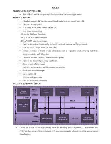
Transcription
User's GuideSLAU319L – July 2010 – Revised May 2016MSP430 Programming With the Bootloader (BSL)The MSP430 bootloader (BSL, formerly known as the bootstrap loader) allows users to communicatewith embedded memory in the MSP430 microcontroller during the prototyping phase, final production, andin service. Both the programmable memory (flash memory) and the data memory (RAM) can be modifiedas required. Do not confuse the bootloader with the bootstrap loader programs found in some digital signalprocessors (DSPs) that automatically load program code (and data) from external memory to the internalmemory of the DSP.To use the bootloader, a specific BSL entry sequence must be applied. An added sequence of commandsinitiates the desired function. A boot-loading session can be exited by continuing operation at a defineduser program address or by the reset condition.If the device is secured by disabling JTAG, it is still possible to use the BSL. Access to the MSP430memory through the BSL is protected against misuse by a user-defined password.MSP430, E2E are trademarks of Texas Instruments.All other trademarks are the property of their respective owners.SLAU319L – July 2010 – Revised May 2016Submit Documentation FeedbackMSP430 Programming With the Bootloader (BSL)Copyright 2010–2016, Texas Instruments Incorporated1
www.ti.com123456ContentsIntroduction . 3Bootloader Protocol – 1xx, 2xx, and 4xx Families. 8Bootloader Protocol – F5xx and F6xx Families . 19Bootloader Hardware . 29Differences Between Devices and Bootloader Versions . 33Bootloader PCB Layout Suggestion . 471Standard RESET Sequence. 52BSL Entry Sequence at Shared JTAG Pins . 53BSL Entry Sequence at Dedicated JTAG PinsList of Figures45678910. 6Basic Protocol - Byte Level ACK . 20Byte Level ACK . 21Bootloader Interface Schematic . 29Universal BSL Interface PCB Layout, Top . 47Universal BSL Interface PCB Layout, Bottom . 47Universal BSL Interface Component Placement . 48Universal BSL Interface Component Placement . 49List of Tables1BSL Overview . 42Data Frame of BSL Commands3Recommendations for MSP430F149 [MSP430F449] (TA 25 C, VCC 3.0 V, fmax 6.7 MHz) . 134Recommendations for MSP430F2131 (TA 25 C, VCC 3.0 V, fmax 6.7 MHz) . 135UART Protocol Interface678910111213141516171819202122232.UART Error Messages.BSL Core Command Wrapper for I2C .USB Peripheral Interface .BSL Core Commands .BSL Core Responses .BSL Core Messages .Serial-Port Signals and Pin Assignments .RS-232 Levels .Pin Assignment of Target Connector .Universal BSL Interface Parts List .BSL Version 1.10 on F13x, F14x(1) (excluding Rev AA), F11x, and F11x1 .BSL Version 1.30 on F41x, F11x, and F11x1 .BSL Version 1.40 on F12x .BSL Version 1.60 on F11x2, F12x2, F43x, F44x, FE42x, FW42x, F43x, FG43x, F415, F417 .BSL Version 1.61 on F16x, F161x, F42x0, F13x rev AA, F14x(1) rev AA, F47x, FG47x .BSL Version 2.02 and 2.13 on F21xx, F22xx, F23xx, F24xx, F261x.BSL Version 2.02 and 2.03 on G2xx3, G2xx4, G2xx5, TCH5E .BSL Version 2.12 and 2.13 on FG46xx, F471xx .MSP430 Programming With the Bootloader (BSL)Copyright 2010–2016, Texas Instruments 0SLAU319L – July 2010 – Revised May 2016Submit Documentation Feedback
Introductionwww.ti.com1IntroductionThe bootloader provides a method to program the flash memory during MSP430 project development andupdates. It can be activated by a utility that sends commands using the UART protocol. The BSL enablesthe user to control the activity of the MSP430 and to exchange data using a personal computer or otherdevice.To avoid accidental overwriting of the BSL code, this code is stored in a secure memory location, eitherROM or specially protected flash. To prevent unwanted source readout, any BSL command that directly orindirectly allows data reading is password protected.To invoke the bootloader, a BSL entry sequence must be applied to dedicated pins. After that, asynchronization character, followed by the data frame of a specific command, initiates the desiredfunction.1.1Supplementary Online InformationAs a compliment to this document, visit Bootloader (BSL) for MSP low-power microcontrollers. This sitecontains links to additional BSL user's guides, source code, firmware images, and the BSL scripter withdocumentation and code examples.Additional support is provided by the TI E2E Community.SLAU319L – July 2010 – Revised May 2016Submit Documentation FeedbackMSP430 Programming With the Bootloader (BSL)Copyright 2010–2016, Texas Instruments Incorporated3
Introduction1.2www.ti.comOverview of BSL FeaturesTable 1 summarizes the BSL features of the MSP devices, organized by device family.Table 1. BSL OverviewGeneralMSP430F5xx, F6xxMSP432FR5xx, nUSBUSBFactoryCryptoBootloader (1)FR2x33,FR231xFR413x,FR211xP401RBSL memory typeNo BSLROMFlash (2)Flash (2)ROMFRAMROMROMFlash (2)BSL memory sizeN/A1KB2KB2KB2KB4K3KB1KB8KB Peripheral configured by TLV UARTI2C SPI Tools SupportInvoke mechanismProtocolUSB '1xx, 2xx, 4xx' protocol '5xx, 6xx' protocol Sequence on TEST/RSTEntry sequenceon I/Os Empty reset vector invoke BSL Calling BSL from software application MSP-FET (3) BSL ScripterBSLDEMO MSPBSL library 32 byteMass erase on incorrect password (5) Completely disable the BSL using signature orerasing the BSL UARTonly UARTonly32 byte(4) 32 byte32 byte32 byte32 byte256 byte BSL payload encryptionUpdate of IP protected regions through bootcode (7)Additional security(2)(3)(4)(5)(6)(7)4 (6) Authenticated encryption(1) MSP-BSL 'Rocket'USB cable(1) Invalid or incomplete applicationHardware PUR pin tied to VUSBPassword protectionSecurity Sequence on defined I/OSoftware All BSL software collateral (application, examples, source code, and firmware images) is available in the BSL tool folder.The MSP430 USB developers package includes additional USB BSL sample applications.BSL in flash memory allows to replace the BSL with a custom version.MSP-FET supports UART and I2C BSL communication only.F543x (non A) has a 16-byte password.Some devices can disable mass erase on incorrect password. See the device family user's guide.The decryption of the payload is performed by the device bootcode.Firmware validation through CRC.MSP430 Programming With the Bootloader (BSL)Copyright 2010–2016, Texas Instruments IncorporatedSLAU319L – July 2010 – Revised May 2016Submit Documentation Feedback
Introductionwww.ti.com1.31.3.1Standard RESET and BSL Entry SequenceMSP430 Devices With Shared JTAG PinsApplying an appropriate entry sequence on the RST/NMI and TEST pins forces the MSP430 to startprogram execution at the BSL RESET vector instead of at the RESET vector located at address FFFEh.If the application interfaces with a computer UART, these two pins may be driven by the DTR and RTSsignals of the serial communication port (RS232) after passing level shifters. Detailed descriptions of thehardware and related considerations can be found in Section 4. The normal user reset vector at FFFEh isused if TEST is kept low while RST/NMI rises from low to high (standard method, see Figure 1).RST/NMI (DTR)TEST (RTS)User Program StartsFigure 1. Standard RESET SequenceThe BSL program execution starts when the TEST pin has received a minimum of two positive transitionsand if TEST is high while RST/NMI rises from low to high (BSL entry method, see Figure 2). This leveltransition triggering improves BSL start-up reliability. The first high level of the TEST pin must be at leasttSBW, En (see device-specific data sheet for tSBW, En parameter).RST/NMI (DTR)TEST (RTS)tSBW,enBootloader StartsFigure 2. BSL Entry Sequence at Shared JTAG PinsNOTE: The recommended minimum time for pin states is 250 ns. See the device-specific errata forany differences, because some 5xx and 6xx device revisions require specific entrysequences.The TEST signal is normally used to switch the port pins between their application function and the JTAGfunction. In devices with BSL functionality, the TEST and RST/NMI pins are also used to invoke the BSL.To invoke the BSL, the RST/NMI pin must be configured as RST and must be kept low while pulling theTEST pin high and while applying the next two edges (falling, rising) on the TEST pin. The BSL is startedafter the TEST pin is held low after the RST/NMI pin is released (see Figure 2).The BSL is not started by the BSL RESET vector if: There are fewer than two positive edges at the TEST pin while RST/NMI is low. JTAG has control over the MSP430 resources. Supply voltage, VCC, drops below its threshold, and a power-on reset (POR) is executed. RST/NMI pin is configured for NMI functionality (NMI bit is set).SLAU319L – July 2010 – Revised May 2016Submit Documentation FeedbackMSP430 Programming With the Bootloader (BSL)Copyright 2010–2016, Texas Instruments Incorporated5
Introduction1.3.2www.ti.comMSP430 Flash Devices With Dedicated JTAG PinsDevices with dedicated JTAG pins use the TCK pin instead of the TEST pin.The BSL program execution starts whenever the TCK pin has received a minimum of two negativetransitions and TCK is low while RST/NMI rises from low to high (BSL entry method, see Figure 3). Thislevel transition triggering improves BSL start-up reliability.RST/NMI (DTR)TCK (RTS)Bootloader StartsFigure 3. BSL Entry Sequence at Dedicated JTAG PinsNOTE: The recommended minimum time for pin states is 250 ns. See the device-specific errata forany differences, because some 5xx and 6xx device revisions have specific entry sequencerequirements.The BSL is not started by the BSL RESET vector if: There are fewer than two negative edges at TCK pin while RST/NMI is low. TCK is high if RST/NMI rises from low to high. JTAG has control over the MSP430 resources. Supply voltage, VCC, drops below its threshold, and a power-on reset (POR) is executed. RST/NMI pin is configured for NMI functionality (NMI bit is set).1.3.3Devices With USBDevices with USB are invoked when either of the following two conditions are met while the device ispowered by VBUS: The device is powered up by USB and the reset vector is blank. The device powers up with the PUR pin tied to VUSB.1.4UART ProtocolThe UART protocol applied here is defined as: Baud rate is fixed to 9600 baud in half-duplex mode (one sender at a time). Start bit, 8 data bits (LSB first), an even parity bit, 1 stop bit. Handshake is performed by an acknowledge character. Minimum time delay before sending new characters after characters have been received from theMSP430 BSL: 1.2 msNOTE: Applying baud rates other than 9600 baud at initialization results in communication problemsor violates the flash memory write timing specification. The flash memory may be extensivelystressed or may react with unreliable program or erase operations.6MSP430 Programming With the Bootloader (BSL)Copyright 2010–2016, Texas Instruments IncorporatedSLAU319L – July 2010 – Revised May 2016Submit Documentation Feedback
Introductionwww.ti.com1.5USB ProtocolThe USB protocol applied here is defined as: HID protocol with one input endpoint and one output endpoint. Each endpoint has a length of 64 bytes. VID: 0x2047 PID: 0x0200SLAU319L – July 2010 – Revised May 2016Submit Documentation FeedbackMSP430 Programming With the Bootloader (BSL)Copyright 2010–2016, Texas Instruments Incorporated7
Bootloader Protocol – 1xx, 2xx, and 4xx Families2Bootloader Protocol – 1xx, 2xx, and 4xx Families2.1Synchronization Sequencewww.ti.comBefore sending any command to the BSL, a synchronization character (SYNC) with its value of 80h mustbe sent to the BSL. This character is necessary to calculate all the essential internal parameters, whichmaintain UART and flash memory program and erase timings. It provides the BSL system time reference.When this is received, an acknowledge DATA ACK 90h is sent back by the BSL to confirm successfulreception.This sequence must be done before every command that is sent to the BSL.NOTE: The synchronization character is not part of the Data Frame described in Section 2.4.2.2CommandsTwo categories of commands are available: commands that require a password and commands that donot require a password. The password protection safeguards every command that potentially allows director indirect data access.2.2.1 Unprotected CommandsReceive passwordMass erase (erase entire flash memory, main as well as information memory)Transmit BSL version (V1.50 or higher or in loadable BL 150S 14x.txt but not V2.x BSLs)Change baud rate (V1.60 or V1.61 or V2.0x or in loadable BL 150S 14x.txt) Password Protected CommandsReceive data block to program flash memory, RAM, or peripheralsTransmit data blockErase segmentErase check (present in V1.60 or higher or in loadable BL 150S 14x.txt)Set Memory Offset (present in V2.12 or higher)Load program counter and start user programChange baud rate (BSL versions lower than V1.60 and higher than V2.10)2.2.22.3Programming FlowThe write access (RX data block command) to the flash memory, RAM, or peripheral modules area isexecuted online. That means a data byte or word is processed immediately after receipt, and the writecycle is finished before a following byte or word has completely arrived. Therefore, the entire write time isdetermined by the baud rate, and no buffering mechanism is necessary.Data sections located below the flash memory area address are assumed to be loaded into the RAM orperipheral module area and, thus, no specific flash control bits are affected.NOTE: If control over the UART protocol is lost, either by line faults or by violating the data frameconventions, the only way to recover is to rerun the BSL entry sequence to initiate anotherBSL session.8MSP430 Programming With the Bootloader (BSL)Copyright 2010–2016, Texas Instruments IncorporatedSLAU319L – July 2010 – Revised May 2016Submit Documentation Feedback
Bootloader Protocol – 1xx, 2xx, and 4xx Familieswww.ti.com2.4Data FrameTo ensure high data security during the data transmission, a data frame protocol called serial standardprotocol (SSP) is used. The BSL is considered the receiver in Table 2.2.4.1 Data-Stream StructureThe first eight bytes (HDR through LH) are mandatory (xx represents dummy data).Data bytes D1 to Dn are optional.Two bytes (CKL and CKH) for checksum are mandatory.Acknowledge done by the BSL is mandatory, except with the TX data block and TX BSL versioncommands.Table 2. Data Frame of BSL Commands (1) (2) (3) (4) (5) (6)ReceivedBSLCommandHDRCMDL1L2ALAHLLLHD1D2 DnCKLCKHACKRX data block8012nnALAHn–40D1D2 Dn–4CKLCKHACKRX password80102424xxxxxxxxD1D2 D20CKLCKHACKErase segment80160404ALAH02A5––––CKLCKHACKErase main or info80160404ALAH04A5––––CKLCKHACKMass erase80180404xxxx06A5––––CKLCKHACKErase check801C0404ALAHLLLH––––CKLCKHACKChange baud rate80200404D1D2D3xx––––CKLCKHACKSet mem offset80210404xxxxALAH––––CKLCKHACKLoad PC801A0404ALAHxxxx––––CKLCKHACKTX data block80140404ALAHn0––––CKLCKH–BSL responds80xxnnD1D2 . . DnCKLCKH–TX BSL version801E0404xxxxxxxx––––CKLCKH–BSL responds80xx1010D1D2 . D10CKLCKH–(1)(2)(3)(4)(5)(6)All numbers are bytes in hexadecimal notation.ACK is sent back by the BSL.The synchronization sequence is not part of the data frame.The erase check and TX BSL version commands are members of the standard command set in BSLs V1.50 or higher butexcluding 2.x BSLs.The change baud rate command is not a member of the standard command set (it is available in V1.60 or higher or in loadableBL 150S 14x.txt).Abbreviations:HDR: Header. Any value between 80h and 8Fh (normally 80h).CMD: Command identificationL1, L2: Number of bytes consisting of AL through Dn. Restrictions: L1 L2, L1 255, L1 evenAL, AH: Block start address or erase (check) address or jump address LO or HI byteLL, LH: Number of pure data bytes (250 max) or erase information LO or HI byte or block length of erase check (FFFFh max)D1 Dn: Data bytesCKL, CKH: 16-bit checksum LO or HI bytexx: Can be any data–: No character (data byte) received or transmittedACK: The acknowledge character returned by the BSL. Can be either DATA ACK 90h: Frame was received correctly,command was executed successfully, or DATA NAK A0h: Frame not valid (for example, wrong checksum, L1 L2), commandis not defined, is not allowed, or was executed unsuccessfully.n: Number of bytes consisting of AL through DnSLAU319L – July 2010 – Revised May 2016Submit Documentation FeedbackMSP430 Programming With the Bootloader (BSL)Copyright 2010–2016, Texas Instruments Incorporated9
Bootloader Protocol – 1xx, 2xx, and 4xx Families2.4.2www.ti.comChecksumThe 16-bit (2-byte) checksum is calculated over all received or transmitted bytes B1 to Bn in the dataframe, except the checksum bytes themselves, by XORing words (two successive bytes) and inverting theresult.This means that B1 is always the HDR byte and Bn is the last data byte just before the CKL byte.FormulaCHECKSUM INV [ (B1 256 B2) XOR (B3 256 B4) XOR XOR (Bn–1 256 Bn) ]orCKL INV [ B1 XOR B3 XOR XOR Bn–1 ]CKH INV [ B2 XOR B4 XOR XOR Bn ]2.4.3Example SequenceThe following example shows a request to read the memory of the MSP430 from location 0x0F00. Allvalues shown below are represented in hexadecimal format.TO BSL:80(Synchronization character sent to the BSL)FROM BSL: 90(Acknowledge from BSL)TO BSL:80 14 04 04 00 0F 0E 00 75 E0(Send Command to read memory from 0x0F00, length 0x000E)FROM BSL: 80 00 0E 0E F2 13 40 40 00 00 00 00 00 00 02 01 01 01 C0 A2(Returned values from BSL)2.4.4Commands – Detailed DescriptionSee Table 2.2.4.4.1GeneralFollowing the header byte HDR (80h) and the command identification CMD, the frame length bytes L1 andL2 (which must be equal) hold the number of bytes following L2, excluding the checksum bytes CKL andCKH.Bytes AL, AH, LL, LH, D1.Dn are command-specific. However, the checksum bytes CKL (low byte) andCKH (high byte) are mandatory.If the data frame has been received correctly and the command execution was successful, anacknowledge character DATA ACK 90h is sent back by the BSL. Incorrectly received data frames,unsuccessful operations, and commands that are locked or not defined are confirmed with a DATA NAK A0h.NOTE: BSL versions lower than V1.30 support only byte-access operations. Therefore, theperipheral module addresses at 0100h to 01FFh cannot be accessed correctly, because theyare word-oriented. In version V1.30 and higher, addresses 0000h to 00FFh are accessed inbyte mode; all others are accessed in word mode.2.4.4.2RX Data BlockThe receive data block command is used for any write access to the flash memory, RAM, or peripheralmodule control registers at 0000h to 01FFh. It is password protected.The 16-bit even-numbered block start address is defined in AL (low byte) and AH (high byte). The 16-biteven-numbered block length is defined in LL (low byte) and LH (high byte). Because pure data bytes arelimited to a maximum of 250, LH is always 0.10MSP430 Programming With the Bootloader (BSL)Copyright 2010–2016, Texas Instruments IncorporatedSLAU319L – July 2010 – Revised May 2016Submit Documentation Feedback
Bootloader Protocol – 1xx, 2xx, and 4xx Familieswww.ti.comThe following data bytes are succeeded by the checksum bytes CKL (low byte) and CKH (high byte). Ifthe receipt and programming of the appropriate data block was successful, an acknowledge characterDATA ACK is sent back by the BSL. Otherwise, the BSL confirms with a DATA NAK.NOTE: BSL versions V1.40 and higher support online verification inside the MSP430 for addresses0200h to FFFFh, which reduces programming and verification time by 50%. Onlineverification means that the data is immediately verified with the data that is written into theflash without transmitting it again. In case of an error, the loadable bootloaderBL 150S 14x.txt additionally stores the first incorrectly written location address 3 into theerror address buffer in the RAM at address 0200h (021Eh for F14x devices).2.4.4.3RX PasswordThe receive password command is used to unlock the password-protected commands, which performreading, writing, or segment-erasing memory access. It is not password protected.Neither start address nor block length information is necessary, because the 32-byte password is alwayslocated at addresses FFE0h to FFFFh. Data bytes D1 to D20h hold the password information starting withD1 at address FFE0h.If the receipt and verification of the password is correct, a positive acknowledge DATA ACK is sent backby the BSL, and the password-protected commands become unlocked. Otherwise the BSL confirms with aDATA NAK.After the protected commands become unlocked, they remain unlocked until another BSL entry is initiated.2.4.4.4Mass EraseThe mass erase command erases the entire flash memory area (main memory plus information memory,see corresponding data sheet). It is not password protected.All parameters shown in Table 2 are mandatory. After erasing, an acknowledge character DATA ACK issent back by the BSL.Mass erase initializes the password area to 32 times 0FFh.NOTE: BSL versions V2.01 and higher support automatic clearing of the LOCKA bit protectinginformation flash memory. When the BSL is entered from a reset condition, LOCKA iscleared by the BSL to mass erase the flash, including information memory. When the BSL isentered in-application, user software should ensure that LOCKA is written as 1 prior toinitiating the BSL. Otherwise, information flash is not erased during a BSL mass erase.2.4.4.5Erase SegmentThe erase segment command erases specific flash memory segments. It is password protected.The address bytes AL (low byte) and AH (high byte) select the appropriate segment. Any even-numberedaddress within the segment to be erased is valid. After segment erasing, an acknowledge characterDATA ACK is sent back by the BSL (V1.40 or lower).BSL versions V1.60 or higher perform a subsequent erase check of the corresponding segment andrespond with a DATA NAK if the erasure was not successful. In this case, the first non-erased locationaddress 1 is stored in the error address buffer in the RAM at address 0200h (021Eh for F14x devices).In this version, a problem occurs if only one of the information memory segments is erased. In this case,an error is reported, because an automatic erase check over the whole information memory is performed.As a solution, either erase the whole information memory or do a separate erase check after the erase,even if the erase reported an error.Erase segment 0 clears the password area and, therefore, the remaining password is 32 times 0FFh.SLAU319L – July 2010 – Revised May 2016Submit Documentation FeedbackMSP430 Programming With the Bootloader (BSL)Copyright 2010–2016, Texas Instruments Incorporated11
Bootloader Protocol – 1xx, 2xx, and 4xx Familieswww.ti.comWhen applying LL 0x04 and LH 0xA5, a mass erasure of only the main memory is performed. Indeed,this command must be executed a minimum of 12 times to achieve a total erasure time of 200 ms. Nosubsequent erase check of the entire main memory is done. Use the erase check command additionally.Check the device data sheet for more information on the cumulative (mass) erase time that must be metand the number of erase cycles required.2.4.4.6Erase Main or InfoThe erase main or info command erases specific flash memory section. It is password protected.The address bytes AL (low byte) and AH (high byte) select the appropriate section of flash (main orinformation). Any even-numbered address within the section to be erased is valid.2.4.4.7Erase CheckThe erase check command verifies the erasure of flash memory within a certain address range. It ispassword protected.The 16-bit block start address is defined in AL (low byte) and AH (high byte). The 16-bit block length isdefined in LL (low byte) and LH (high byte). Both can be either even or odd numbered to allow oddboundary checking.If the erase check of the appropriate data block was successful (all bytes contain 0FFh), an acknowledgecharacter DATA ACK is sent back by the BSL. Otherwise, the BSL confirms with a DATA NAK and thefirst non-erased location address 1 is stored in the error address buffer at address 0200h (021Eh forF14x devices).NOTE: This command is not a member of the standard command set. It is implemented in BSLversion V1.60 and higher or in the loadable bootloader BL 150S 14x.txt.2.4.4.8Change Baud RateThe change baud rate command offers the capability of transmissions at higher baud rates than thedefault 9600 baud. With faster data transition, shorter programming cycles can be achieved, which isespecially important with large flash memory devices. This command is not password protected.Three control bytes (D1 to D3) determine the selected baud rate. D1 and D2 set the processor frequency(f fmin), D3 indirectly sets the flash timing generator frequency (fFTGmin fFTG fFTGmax). In detail:D1: F1xx: Basic clock module control register DCOCTL (DCO.2 to DCO.0)F2xx: Basic clock module control register DCOCTL (DCO.2 to DCO.0)F4xx: FLL system clock control register SCFI0 (D, FN 8 to FN 2)D2: F1xx: basic clock module control register BCSCTL1 (XT2Off, Rsel.2 to Rsel.0)F2xx: basic clock module control register BCSCTL1 (XT2Off, Rsel.2 to Rsel.0)F4xx: FLL system clock control register SCFI1 (NDCO)D3 0: 9600 Baud1: 19200 Baud2: 38400 BaudAfter receiving the data frame, an acknowledge character DATA ACK is sent back, and the BSL becomesprepared for the selected baud rate. TI recommends that the BSL communication program waitapproximately 10 ms between baud rate alteration and the next data transmission to give the BSL clocksystem time to stabilize.NOTE: The highest achievable baud rate depends on various system and environment parameterslike supply voltage, temperature range, and minimum and maximum processor frequency.See the device-specific data sheet.12MSP430 Programming With the Bootloader (BSL)Copyright 2010–2016, Texas Instruments IncorporatedSLAU319L – July 2010 – Revised May 2016Submit Documentation Feedback
Bootloader Protocol – 1xx, 2xx, and 4xx Familieswww.ti.comNOTE: This command is implemented on BSL versions V1.60 or higher or available in the loadablebootloader BL 150S 14x.txt.Table 3. Recommendations for MSP430F149 [MSP430F449] (1)(TA 25 C, VCC 3.0 V, fmax 6.7 MHz)(1)(2)(3)(4)Baud Rate(Baud)ProcessorFrequency, fmin(MHz) (2)D2 BCSCTL1[SCFI1] (3)D3 (3)Program andVerify 60 KB(sec) (4)9600 (init)1.05192002.10x80 [00]0x85 [98]00 [00]78 3.7 [0.0]0xE0 [00]0x86 [B0]01 [01]384004.20xE0 [00]39 3.7 [2.4]0x87 [C8]02 [02]20 3.7 [2.4]D1 DCOCTL[SCFI0] (3)Values in brackets [ ] apply to MSP430F449.The minimum processor frequency is lower than in the standard ROM BSL (see Section 2.9.3, Initialization Status).D1 to D3 are bytes in hexadecimal notation.Additional 3.7 [2.4] seconds result from loading, verifying, and launching the loa
MSP430 Programming With the Bootloader (BSL) 1.3 Standard RESET and BSL Entry Sequence 1.3.1 MSP430 Devices With Shared JTAG Pins Applying an appropriate entry sequence on the RST/NMI and TEST pins forces the MSP430 to start program execution at the BSL RESET vector instead of at the RESET vector located at address FFFEh.