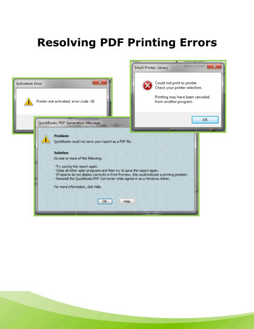
Transcription
DC/DC Converter OutputCapacitor BenchmarkR. Šponar, R. Faltus, M. Jáně, Z. Flegr, T. ZedníčekAVX Czech Republic s.r.o., Dvorakova 328, 563 01 Lanskroun, Czech Republicemail: e power supplies (SMPS) are commonly found in many electronicsystems. Important SMPS requirements are a stable output voltage with loadcurrent, good temperature stability, low ripple voltage and high overall efficiency.If the electronic system in question is to be portable, small size and light weightare also important considerations. A key component in switching power systemsis the output capacitor – used to store the charge and for smoothing - thereforeits careful selection plays a vital role in determining the overall parameters of thepower supply. Different capacitor technologies – tantalum, ceramic MLCC,niobium oxide (NbO) and aluminium - are suitable to meet different electricalrequirements.This paper presents the results of an output capacitor benchmark study used in astep-down DC/DC converter design, based on a well-used control IC (Maxim’sMAX 1537 – Ref.1) with a 6-24V input voltage range and two separate voltageoutputs of 3.3 and 5V. The behaviour of different output capacitor technologieswas evaluated by measuring the output ripple voltage. Defined fixed load andfixed switching frequency settings were used for all measurements.
IntroductionThe selection of a suitable output capacitor plays an important part in the design of switching voltageconverters. “Some 99 percent of so-called ‘design’ problems associated with linear and switching regulatorscan be traced directly to the improper use of capacitors”, states the National Semiconductor IC PowerHandbook (Ref.2). The importance of the output capacitor in switching DC/DC converters is related to the factthat it is (together with the main inductor) the reservoir of electric energy flowing to the output and it smoothesthe output voltage.Today, one can hardly find a consumer, industrial or high reliability electronic device that does notmake use of a voltage regulator. Designers basically use two types of regulators, linear LDO (low dropout) andstep-down switch-mode DC/DC regulators to convert voltage to lower level. Switching DC/DC regulators arepreferred for applications that require a greater difference between input and output voltages because they aremore efficient. This switching regulator option has been selected for our experimental measurements as it is themost commonly used approach in today’s power supply circuits.Frequency Dependence of Capacitance, ESR (effective serial resistance) and stability withoperational temperature and DC bias voltage are the important parameters of output capacitors, definingperformance and functionality of the complete power system. Therefore, it is these key parameters that havebeen measured using different capacitor technologies for the purpose of benchmarking.Notebook computers provide one of the most demanding electronics applications where DC/DCconverters are typically used with high output current requirements. Notebook supply voltages usually rangebetween 15 and 22V with 3.3 and 5 V internal power buses commonly seen. To satisfy market demand,semiconductor manufacturers offer integrated DC/DC controllers optimized for these voltage ranges. Suchcontrollers, soldered on a PCB together with all necessary passive and discrete components function asDC/DC converters with maximal output currents of up to several amperes. One notebook power supplyconverter evaluation kit, based around Maxim’s MAX1537 has been chosen as a real application example forthe evaluation of different capacitor technologies.Switched-mode power supply (SMPS) – theory and simulationsTypical SMPS topologies are shown in Figure 1. They are well documented (Ref.3).SMPS are used for VIN-to-VOUT transformation: VOUT VIN, realized by step-up, flyback or SEPIC converters; VOUT VIN, realized by step-down, flyback or SEPIC converters; VOUT VIN, realized by flyback or SEPIC converters; VOUT -VIN, realized by an inverting converter.An SMPS circuit consists of these specific parts: one or more switching transistors, mainly enhancement-mode MOSFETs; input and output smoothing capacitors;2
low-loss passive device(s) accumulating electromagnetic energy (inductors, capacitors, transformers); non-linear rectifying devices (plain P-N or Schottky diodes); control sub-circuitry for switching transistor management, feedback stability, and shut-down functionality.a)b)c)d)e)f)g)h)Figure 1: Typical SMPS topologies:a) Step-down (buck) converterb) Synchronous step-down (buck) converterc) Step-up (boost) converterd) Synchronous step-up (boost) convertere) Synchronous step-down-up (buck-boost) converterf) Single ended primary inductor converter (SEPIC)g) Flyback isolated-output converterh) Inverting converter (inverter)The SMPS function actually lies in the periodic repetition of charging and discharging cycle parts (pulse-widthmodulation – PWM) when the passive accumulating device(s) is (are) shortly connected to the input or outputvia the switching MOSFET. Switching duty cycle is the fundamental factor for VIN-to-VOUT transformation, i.e.determines the VOUT value with respect to the VIN value. Voltage drops and switching times of both rectifyingdiodes and switching MOSFETs are critical due to thermal parasitic losses.Figure 2 shows a basic simulation scheme with a step-down SMPS topology based on MAX1537 Evaluation Kit3
(Ref.4). OrCAD simulations express output voltage ripple dependencies on switching conditions and outputcapacitor properties. The circuit parameters are as follows:Rinput 0.1 Ω, Cin 10 µF, Lin 3 nH, Rin 0.1 Ω, Cinter 100 nF, Lser 6 µH,Cout 1 mF ( basic value ) , Lout 3 nH, Rout ESR 10 mΩ ( basic value ) , Rload 1 Ω,MOS Switch: Ron 25 mΩ, Roff 1 MΩ, tswitch 2.5 ns, tdelay 35 ns.Figure 2: SMPS simulation schemeFigure 3 shows that the output voltage ripple depends on the switching frequency and the duty cycle factor. VDCwas set at 7V. Obviously the optimal switching frequency lies between 100 kHz and 1MHz while the duty cyclefactor linearly affects the DC output voltage.Figure 3: SMPS output voltage ripple (dependent on frequency and duty cycle)Figure 4 shows the output voltage ripple dependency on output capacitor ESR and capacitance. VDC was set at20V, switching frequency is 300 kHz and the duty cycle is 17%. The lowest ripple values can be obtained when100µF C 1mF and ESR 0.1Ω are used.4
Figure 4: SMPS output voltage ripple (dependent on output capacitor ESR and C)Low Drop-Out Regulator (LDO) - theory and simulationsThere are two functions of a capacitor connected to the output of an LDO: Local electrical energy reserve RF noise coupling to ground Feedback stability factor for LDOA simplified structure of an LDO with external input/output capacitor and feedback resistors is shown in Figure5.Figure 5: Simplified LDO and typical external componentsIt is commonly known that the output capacitor influences the stability of an LDO with a connected load(assumed to be pure resistive). Note that the type of switching transistor used in the LDO structure correspondsto the orientation of positive /negative inputs of an amplifier within the LDO feedback loop. The followingtransistors can be utilized: NPN or PNP in case of BJT; and N-channel or P-channel in case of enhancementand depletion mode MOS. NPN and N-channel MOS transistors are implemented as shown in Figure 5; PNPand P-channel MOS require the amplifier inputs to be swapped. The feedback is designed to lead the voltagesignal from the voltage R2/(R2 R1) divider to the signal-error voltage amplifier (both VFA and CFA), which is DC5
biased on one input and asymmetrically supplied (VIN to GND).We are able to describe LDO properties that may influence the LDO feedback stability: input impedance of the feedback amplifier (much greater than both the external feedback resistors R1, R2); parasitic grounded impedance of connected open output mirror and voltage follower; input impedance of the feedback amplifier (much lower than the input impedance of the switchingtransistor); switching transistor parameters, mainly gate-source, gate-drain and drain-source capacitance; frequency characteristics of the over-current feedback loop.Major aspects playing an important role in LDO feedback stability will be analysed: two-pole amplifier (single-pole, unity-gain voltage followers, single-pole, open output current mirror); Giacoletto model of switching MOS transistor (based on voltage-controlled current source)The LDO stability is often evaluated from the open loop scheme shown in Figure 6.Figure 6: Open loop gain & phase measurement of LDO with external resistive divider, output capacitor andloadThe voltage open loop transfer function can be stated as follows:ΚV 2 π fb1gg a mCdss 2 π f b Cgd s 1Cgd Rgds 1Cout Resr 1 R R (R1 R2 ) s s Cout Resr Cds 1ds 1load 1 s C Rds esr R2,R1 R2where fB is a dominant pole frequency of the feedback voltage buffer, ga is a gain of the feedbacktransconductance amplifier, and gm is the transconductance gain of the Giacoletto model of the switching MOStransistor. The ‘gd’ and ‘ds’ index refers to the MOS gate-drain and drain-source resistance/capacitancerespectively. Resr and Cout represent the elementary model of the output capacitor and Rload means the resistive6
load.If a designer adds a capacitor to the LDO output, the voltage open loop transfer function changes with the ratio:R K V, with capacitorK V, without capacitor 1 sCds Resr 1 1 sR 1 Rload1 (R1 R2 ) s s ds Cds Resr CdsCRoutesr .The reader can confirm that in the case Resr Ω or Cout 0 F the R 1.KV function of LDO without the output capacitor contains plain real poles with characteristic frequencies: 1 (R1 R2 )1R 1 Rload, f p 3 ds2 π Cgd Rgd2 π Cds 1f p1 f b , f p 2 [Hz].Adding the output capacitor we obtain the plain real zero (fz1) and the pseudo-pole (fp4) due to s/CdsResrelement:f z1 11[Hz]., fp 4 2 π Cout Resr2 π Cout ResrDue to the pseudo-pole existence, the single zero is not eliminated by the pseudo-pole and has an ability toincrease the LDO stability.The well-known Bode criterion states that a feedback electrical system is stable if the open loop magnitudecurve crosses unity-gain level with a maximum slope of less than 30 dB/decade. Absolute stability is obtainedwhen the slope is lower or equal to 20 dB/decade, therefore the unity gain phase margin is positive.Let us assume following numerical values of the scheme shown in Figure 6:f b 10 kHz, g a g m 100 mS, Cgd 100 pF, Rgd 10 M Ω, Cds 1 nF, Rds Rload 10 Ω,R1 10 k Ω, R2 1 k Ω, Cout 〈10 nF; 1 mF〉 , Resr 〈1 m Ω; 100 Ω〉.If the typical value of DC reference voltage is Vref 1.25 V, then the output DC voltage and output load currentis:Vout Vref R1 R2V 13.75 V, I out out 1.375 A .R2RloadThe numerical values of pole characteristic frequencies of LDO without the output capacitor are as follows:f p 1 10 kHz, f p 2 159 Hz, f p 3 31.8 MHz .An LDO application designer should know the capacitance and ESR of the output capacitor. Figure 7 showshow the unity gain frequency (transient frequency) changes with varying Cout and Resr. It appears that by usingas high capacitance and as low ESR as possible leads to the lowest transient frequency.7
Figure 7: Capacitance and ESR of output capacitor influence unity gain frequency of LDO regulation loopFigure 8 displays an example of LDO open loop phase margin at 1 MHz and proves the phase margininsensitivity to ESR changes, especially for Cout 100 µF. The transient frequency point may be lower orgreater than 1 MHz (dependent certainly on Cout and ESR). As a worst case scenario, we need the positivephase margin for the band up to the transient frequency. Figure 8 proves that a too low ESR solution leads toundesired negative phase margin at lower Cout.Figure 8: LDO regulation loop phase margin @ 1 MHz8
Figure 9 shows the real worst case phase margin and was obtained using iterative computations over thetransient frequency space. The phase margin is always positive if Cout 100 µF, Resr 0.1 Ω. This conclusionis certainly valid only for the given numerical values of internal LDO parameters as well as external properties(i.e. resistive feedback voltage divider and output load). Both Cout and Resr fundamentally change a zero pointposition and thus shift the phase margin value in the positive-gain band.Figure 9: Worst case: LDO open loop phase margin @ unity gain frequencyPrevious symbolic and numerical computations as well as 3D graphs gave the answer to the question: “Howwill a capacitor affect the LDO stability.” It is clear that an LDO application designer should search for a validLDO model and verify the LDO stability in two ways: Open loop AC stability analysis (gain & phase margin evaluation); Steep input edge transient analysis of the output signal stability and settling (power-on testing).A numerical circuit simulation with precise LDO/SMPS and output capacitor models gives more credible resultsin a shorter time than elaborating rigorous semi-symbolic computations as shown above. The previousmathematical apparatus only wants to show the possibility to guess the right Cout and ESR values.Measurement set-upInitially, the frequency characteristics of capacitance and ESR of two capacitor groups was measured. The firstgroup included different capacitors specified for the 3.3V output with capacitance C 220µF; the second groupcontained capacitors for the 5V output where C 150µF. Electrical parameters were measured using an HP4194A impedance/gain-phase analyser (Ref. 5) in a frequency range of 120Hz to 1MHz (capacitance) and120Hz to 10MHz (ESR).The temperature stability of the converter is one of industry’s most common requirements. Thus, the secondmeasurement concentrated on capacitance and ESR stability with temperature and DC voltage bias. The 3.3Voutput capacitor group was measured using an HP 4192A impedance analyser and a Keithley 7002 switch9
system across the DC bias, voltage range 0 – 4V, conditioned in a Votsch VC 7018 laboratory oven over thetemperature range of -55 to 125degC.Maxim Integrated Product’s MAX1537EV KIT (Ref. 4) converter was used for the benchmarking tests. Theevaluation kit provides two power outputs, 3.3 and 5 V, both with a maximum current Iout of 5A. A photograph ofthe kit is shown in Figure 10. The recommended output capacitance, C, for the 3.3V output is 220µF (seeposition C6 in Figure 11); for the 5V output the value of C is 150µF. AC ripple voltage values and wave formswere used as the main indicator of filtering quality. A Goldstar GP-505 stabilized power supply was used tosupply the kit with a fixed input voltage Vin of 20V.Figure 10 : MAX1537EV evaluation kitFigure 11 : Section of the MAX1537EV evaluation kit schematic diagram with 3.3V output10
An output load was set up using resistors and capacitors to draw two thirds of the maximum current. (For 3.3Voutput this was a parallel combination of 2.2 Ω resistor (R) and 4.7µF tantalum capacitor (C); for the 5V outputthe value of R 3.2Ω (see Figure 12). Voltage waveforms and relevant AC Vrms (effective value) weredisplayed using an Agilent Infiniium 54830B digital oscilloscope (Ref. 6).Figure 12 : MAX1537EV evaluation kit measurement connection diagramFrequency characteristics of various capacitors used for 3.3 V outputCapacitanceTa-Polymer (Y220/6)Ta-MnO2 (Y220/6)NbO-MnO2 (D220/6)Ta-MnO2 (D220/10, multi)MLCC X5R (2x100/4)AlEl (220/16)250.0Cap [µF]200.0150.0100.050.00.01001 00010 000frequency [Hz]100 0001 000 000Figure 13 : Capacitance vs. frequency of various capacitors for 3.3V output11
ESR1.000Ta-Polymer (Y220/6)Ta-MnO2 (Y220/6)NbO-MnO2 (D220/6)Ta-MnO2 (D220/10, multi)MLCC X5R (2x100/4)AlEl (220/16)ESR [Ohm]0.1000.0100.0011001 00010 000100 000frequency [Hz]1 000 00010 000 000Figure 14 : ESR vs. frequency of various capacitors for 3.3V outputThe graphs above show the frequency characteristics of several different technology capacitors used for the3.3V evaluation kit output with nominal capacitance C 220µF (except MLCC where two parallel 100µF wereused). The capacitor technologies chosen were Tantalum-Polymer, Tantalum-MnO2 (single and multi-anodeconstruction), Niobium Oxide-MnO2, Multilayer Ceramic, and Aluminium Electrolytic.We can observe a relatively small drop in capacitance in the frequency range 10 – 100kHz in thecase of Tantalum-Polymer and Tantalum-MnO2 multi-anode construction capacitors (see Figure 15), whereasTantalum-MnO2 and Aluminium-electrolytic capacitors exhibit a larger drop across the same range. The actualcapacitance of the MLCC capacitor suffers due to its dependence on the DC bias voltage, which was appliedduring measurement. The very low ESR performance of the MLCC parts, and still relatively low ESR of theTantalum-Polymer capacitors is shown in Figure 16. The ESR of Aluminium-electrolytic capacitors is relativelyhigh over the complete measured frequency range.12
Frequency characteristics of various capacitors chosen for 5V outputMnO2-Polymer (Y150/6)CapacitanceTa-MnO2 (D150/10)200.0NbO-MnO2 (D150/6)180.0Ta-MnO2 (E150/16, multi)MLCC X5R (100/6)160.0AlEl (100/25)Cap [µF]140.0120.0100.080.060.040.020.00.01001 00010 000frequency [Hz]100 0001 000 000Figure 15 : Capacitance vs. frequency of various capacitors for 5V outputESRMnO2-Polymer (Y150/6)10.000Ta-MnO2 (D150/10)NbO-MnO2 (D150/6)Ta-MnO2 (E150/16, multi)MLCC X5R (100/6)ESR [Ohm]1.000AlEl (100/25)0.1000.0100.0011001 00010 000100 000frequency [Hz]1 000 00010 000 000Figure 16 : ESR vs. frequency of various capacitors for 5V outputThe graphs above show the frequency characteristics of different technology capacitors used with the 5Vevaluation kit output with nominal capacitance (C) of 150µF (except MLCC (100µF) and AlEl (100µF)).(Technologies as for the 3.3V output tests, detailed in the paragraph above.)Both Tantalum-MnO2 single and multi-anode capacitors retain a higher capacitance at higherfrequencies (above 100kHz), whereas Niobium Oxide-MnO2 and Aluminium electrolytic capacitors lose theircapacitance faster at lower frequencies (see Figure 15). MLCC exhibits very low ESR around the 100kHzfrequency range; Tantalum-MnO2 multi-anode and Tantalum-Polymer capacitors show low ESR in the same13
frequency range, whereas Aluminium electrolytic devices have a high ESR over all frequency ranges.Capacitance stability vs. DC bias voltage and temperatureTa-MnO2 (case Y 220µF / 6V)Ta-Polymer (case Y 220µF / 6V)Graph of Capacitance stabilityGraph of Capacitance stability7060807060-55500125Temperature [ C]DC Bias [V]4Temperature [ C]NbO-MnO2 (case D 220µF / 6V)2DC Bias [V]4MLCC X5R (2 x 100µF / 4V)Graph of Capacitance stabilityGraph of Capacitance e [ C]-25-555005-2550100DC Bias [V]Temperature [ C]21259011095100120651105Relative Capacitance [%]130120-55Relative Capacitance 5Relative Capacitance [%]130120-55Relative Capacitance [%]1304DC Bias [V]AlEl (220µF / 16V )Graph of Capacitance stability12011010090807060125Temperature [ C]295655035-2550-55Relative Capacitance [%]1304DC Bias [V]Figure 17 : Capacitance stability of various capacitors for the 3.3V evaluation kit outputThe experiments showed that the best overall capacitance stability is exhibited by Tantalum-MnO2 technology14
capacitors (see Figure 17). The capacitance of Niobium Oxide-MnO2 devices is more sensitive to DC biasvoltage, while Tantalum-Polymer is more sensitive to temperature changes. The capacitance of MLCC devicesis very dependent on both actual temperature and DC bias. The capacitance of Aluminium electrolyticcapacitors is stable with DC bias but very dependent on temperature.ESR stability vs. DC bias voltage and temperatureTa-MnO2 (case Y 220µF / 6V)Ta-Polymer (case Y 220µF / 6V)Graph of ESR stabilityGraph of ESR stability100.0ESR [mOhms]ESR [mOhms]100.010.0NbO-MnO2 (case D 220µF / 6V)95Temperature [ C]2DC Bias [V]4125125DC Bias [V]465352956535Temperature [ C]05-25-5505-55-2510.0MLCC X5R (2 x 100µF / 4V)Graph of ESR stabilityGraph of ESR stability10.0ESR [mOhms]ESR [mOhms]100.01.095Temperature [ C]6535DC Bias [V]2125125405-55295Temperature [ C]65355-25-550-250.110.04DC Bias [V]AlEl (220µF / 16V)Graph of ESR stabilityESR [mOhms]100000.010000.01000.0100.00125Temperature [ C]29565355-25-5510.04DC Bias [V]Figure 18 : ESR stability of various capacitors dedicated for 3.3 V evaluation kit output15
We can see that ESR is relatively stable vs. DC bias voltage for all capacitors. However, differences can beseen when we compare ESR stability versus temperature (see Figure 18). Tantalum-Polymer and MLCCcapacitors exhibit the most stable ESR, and the ESR of MLCC devices is very low over the whole temperaturerange. With Tantalum-MnO2 and Niobium Oxide-MnO2 components, ESR decreases as temperature increases.Aluminium electrolytic capacitors behave differently: ESR grows to very high values at low temperatures (below0degC), due to the limitation of wet electrolyte conductivity at low temperatures.DC/DC converter output ripple voltage waveform3.3 V line – Ta-Polymer (case Y 220µF / 6V)3.3 V line – MLCC X5R (2 x 100µF / 4V)3.3 V line – Ta-MnO2 (case Y 220µF / 6V)3.3 V line – AlEl (220µF / 16V)Figure 19 : Output ripple current waveforms on the 3.3V rail with selected capacitors5 V line – Ta-Polymer (case Y 150µF / 6V)5 V line – NbO-MnO2 (case D 150µF/ 6V)16
5 V line – MLCC X5R (100µF / 6V)5 V line – AlEl (100µF / 25V)Figure 20 : Output ripple current waveforms on the 5V rail with selected capacitorsFigure 19 and Figure 20 show the different waveform shapes that occur when different capacitors types areused. Comparing Tantalum-Polymer and Tantalum-MnO2 capacitors shows that the ripple voltage usingTantalum-MnO2 devices contains a lower level of higher harmonic components for both 3.3 and 5V outputs.The basic frequency of the ripple voltage is naturally equal to the switching frequency of the converter (fsw 300 kHz). When using MLCC capacitors, both 3.3 and 5V circuits exhibited undesirable oscillations (foscapproximately 50 kHz) and high AC Vrms due to the regulator instability. Aluminium electrolytic types did notperform well, as can be seen on the waveforms of both outputs measured by a relatively high AC Vrms.Temperature effect on output ripple voltageRipple voltage 3.3V line - VrmsRipple voltage 3.3V line - Vrms16032AC Vrms [mV]120100NbO-MnO2 (D220/6)31Ta-MnO2 (D220/10, multi)30MLCC X5R (2x100/4)29AC Vrms [mV]140AlEl (220/16)8060Ta-Polymer (Y220/6)Ta-MnO2 (Y220/6)NbO-MnO2 (D220/6)Ta-MnO2 (D220/10, e [ C]10203040Temperature [ C]Figure 21 a:b:3.3V output Vrms of ripple voltage benchmark, magnified scale on right side17506070
Ripple voltage 5V line - VrmsRipple voltage 5V line - Vrms19535MnO2-Polymer (Y150/6)33155NbO-MnO2 (D150/6)31135Ta-MnO2 (E150/16, multi)29AC Vrms [mV]AC Vrms [mV]175MLCC X5R (100/6)115AlEl (100/25)9575Ta-MnO2 (D150/10)NbO-MnO2 (D150/6)Ta-MnO2 (E150/16, ure [ C]10203040506070Temperature [ C]Figure 22 a:b:5V output Vrms of ripple voltage benchmark, magnified scale on right sideAluminium electrolytic and MLCC capacitor Vrms behaviour across a wide Vrms range is displayed in Figure21a and Figure 22a . Figure 21b and Figure 22b show a much smaller range in magnified scale. For bothoutputs and most of the capacitor technologies the output ripple Vrms decreases with increasing temperature ina nearly linear fashion. Aluminium electrolytic and MLCC capacitors are exceptions due to the exponentialchange in capacitance and ESR they exhibit with temperature (see Figure 17 and Figure 18). Aluminiumelectrolytic capacitors also exhibit a too high level of ESR across the temperature range, so their smoothingability is limited, as the output ripple voltage is much higher than with other technologies. When MLCC is usedwith the very low ESR levels circuit instabilities result, so output ripple voltage is also high. Among the othertechnologies we can observe that ripple voltage at the output will be lower when ESR is low and capacitance atswitching frequency is high.SummaryTable of output capacitor preliminary static measurementsCapacitortechnologyTa-PolymerTa-MnO2 (single)NbO-MnO2Ta-MnO2 (multi)MLCCAluminium El.Explanation:Level of the ESRat fsw 300 kHz - (too low)- (too high) very good,Capacitancestabilitytemperature 0- good,vs.0 neutral,18Capacitancestability vs.voltage bias - poorDCESR stability vs.temperature -
Table showing output capacitor application measurementsCapacitor technologyAC Vrms at 25 CTa-PolymerTa-MnO2 (single)NbO-MnO2Ta-MnO2 (multi)MLCCAluminium El.Explanation:-Vrmsstabilitytemperature 0 - 0 very good, good,0 neutral,vs.Case size 0 -- poorLow output ripple voltage for the DC/DC converter can be achieved using output capacitors withlow ESR at the switching frequency - in our case Tantalum-polymer and Tantalum-MnO2 multianode capacitors. The rate of decrease of the actual capacitance with frequency in relation to theresonance frequency is also important.-Tantalum-MnO2 capacitors are recommended in applications with variable output voltages becausethey offer the best capacitance stability versus DC bias voltage.-It is strongly recommended that designers consider the capacitance and ESR temperature stabilityof output capacitors when deciding on the system’s operating temperature. From this point of view,Tantalum-Polymer and Tantalum-MnO2 capacitors were found to be the most stable, whereasMLCC and Aluminium-electrolytic capacitor are the least stable.-Comparing capacitor size: in our benchmark, Tantalum-Polymer and Tantalum-MnO2 low profilecapacitors were the smallest suitable capacitors followed by Niobium Oxide-MnO2 with the samefootprint but a little higher in profile. Aluminium-electrolytic radial leaded capacitors require a biggerfootprint and are much larger in volume.Conclusions and Recommendations-As the main energy carrier, the output capacitor plays an important role in DC/DC switchingconverter functionality. The capacitance and ESR of the output capacitor can significantly influencethe DC/DC converter regulator feedback loop, which defines the stability of the converter operation.These parameters have to be in a certain range to assure stability of the system. In ourexperiments, MLCC output capacitors had too low an ESR (in range of 1 – 2mΩ), which resulted inoscillations of the circuit and a relatively high ripple voltage. Therefore, MLCC devices cannot berecommended based on the findings of our experimental study. The use of MLCC capacitors canbe recommended only following a careful evaluation of their low ESR versus stability of the loop.-Using of generic Aluminium electrolytic capacitors resulted in high output ripple voltage and poorfiltering due to their higher ESR characteristics. This also significantly deteriorates at lowertemperatures.-Based on our measurements using the Maxim MAX1537EVKIT evaluation kit we can conclude that19
using low ESR output capacitors such as Tantalum-Polymer and Tantalum-MnO2, especially with amulti-anode construction, leads to the best results measured by AC Vrms of output ripple voltageand Vrms temperature stability. MLCC and Aluminium Electrolytic technologies can be used aslong as attention is paid to the instability (MLCC) and output ripple (Aluminium). Good cost versusperformance value can be also achieved using NbO capacitors.References1] Maxim MAX1537 main power supply controller datasheet and product flyer: http://www.maximic.com/quick view2.cfm/qv pk/45212] C. Simpson, Member of Technical Staff, Power Supply Design Group, National Semiconductor3] SMPS datasheets from Maxim, National Semiconductor, Linear Technology, ON Semiconductor, TexasInstruments and other SMPS manufacturers, available at:http://www.maxim-ic.com/products/power/dc dc ple navId ons/parametrics.do?id search.tsp?family analog&familyId 490&uiTemplateId NODESTRY PGE T4] Maxim MAX1537EVKIT evaluation kit datasheet and product flyer: http://www.maximic.com/quick view2.cfm/qv pk/45465] HP Impedance analyser 4192A description and m6] Agilent Infiniium oscilloscope 54830B t2/9/0o4ptsp0alkuqg2rh3tp0wy3expy.pdf7] T. Zednicek, B. Vrana et al., Tantalum and Niobium Technology pdf8] T. Zednicek, Tantalum Polymer and Niobium Oxide t.pdf20
21
Figure 4 shows the output voltage ripple dependency on output capacitor ESR and capacitance. V DC was set at 20V, switching frequency is 300 kHz and the duty cycle is 17%. The lowest ripple values can be obtained when . two-pole amplifier (single-pole, unity-gain voltage followers, single-pole, open output current mirror);