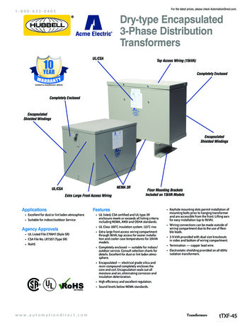
Transcription
This article has been accepted for publication in a future issue of this journal, but has not been fully edited. Content may change prior to final publication. Citation information: DOI 10.1109/JESTPE.2019.2891317, IEEE Journalof Emerging and Selected Topics in Power ElectronicsHigh-Frequency Three-Phase Interleaved LLC Resonant Converter withGaN Devices and Integrated Planar MagneticsChao Fei, Member, IEEE, Rimon Gadelrab, Student Member, IEEE, Qiang Li, Member, IEEE, Fred C. Lee, LifeFellow, IEEECenter for Power Electronics SystemsVirginia Tech, Blacksburg, VA 24061 USAAbstract— The LLC converter is deemed the most widelyused topology as DC/DC converter in server and telecomapplications. To increase the output power and reduce theinput and output current ripples, three-phase interleavedLLC converter is becoming more and more popular. It hasbeen demonstrated that three interleaved LLC convertercan achieve further efficiency improvement at the 3kWpower level. However, the magnetic components formultiphase LLC converter are complex, bulky, anddifficult to manufacture in a cost-effective manner. In thispaper, a high-frequency GaN based three-phase LLCconverter is employed to address these aforementionedchallenges. With GaN operating at 1MHz, all magneticscomponents, namely, 3 inductors and 3 transformers, canbe integrated in one common structure while all magneticwindings implemented in a compact 4-layer PCB with 3ozcopper. The proposed structure can be rthermore, shielding techniques for full-bridgesecondary has been investigated, and additional 2-layershielding has been integrated to reduce common-mode(CM) noise. A 1MHz 3kW 400V/48V three-phase LLCconverter is demonstrated, and peak efficiency of 97.7%and power density of 600W/inch3 (37kW/L) are achieved.frequency fS with better efficiency, resulting in a higher powerdensity and lower total cost [2][4].With the fast development of information technology (IT),the total power consumption of today’s data centers isbecoming noticeable. In 2014, data centers in the U.S.consumed an estimated 70 billion kWh, representing about1.8% of total U.S. electricity consumption [7]. Moreover, ascloud computing and big data are continuing to growingrapidly, data centers is expected to consume more and moreenergy. The current practice of data center power architecture isillustrated in Fig. 1(a), where all major processor/memorydevices are powered from a 12V bus. Such structure has limitedtotal system efficiency due to many energy conversion stagesand large copper loss at 12V bus, and high cost for connectorsand bus bar at 12V bus. To mitigate the heavy bus-bar loss andreduce energy conversion stages in the power distribution path,Google is promoting a new data center design with 48Vdistribution bus instead of 12V bus [8]-[13]. Power architecturewith 48V bus, shown in Fig. 1(b), has the benefits of lessdistribution losses at 48V bus compared to 12V bus,compatibility with 48V telecom power supply ecosystem, costeffective in-rack uninterruptible power source (UPS), and safebus bar voltage for human body.Keywords— LLC resonant converter, interleaving,magnetic integration, high-frequency transformer, galliumnitride (GaN).I.INTRODUCTIONThe LLC converter is the most widely used topology asDC/DC converter for front-end power supplies in server andtelecom applications. The LLC resonant converters have thebenefit of zero-voltage-switching (ZVS) for all the loadconditions, can maintain a low turn-off current for primaryswitches and zero-current-switching (ZCS) for the synchronousrectifiers (SRs), thus LLC converter can achieve both highefficiency and high power density [1]-[6]. Since LLC converterhas small turn-off current, the dv/dt at the primary switchingnode is also small, which helps reduce electromagneticinterference [5]. In comparison with soft-switching PWMconverters, LLC converters can achieve a higher switchingThis work was supported by the Power Management Consortium in theCenter for Power Electronics Systems (CPES), Virginia Tech.(a)(b)Fig. 1 Comparison of data center power architectures. (a) Current architecturewith 12V bus. (b) Alternative architecture with 48V bus.In datacenter architecture with 12V bus, most AC/12V PSUare designed for 1kW output power [14]. As power demand fordatacenter architecture keeps increasing, the AC/48V PSU isnormally designed for 3kW output power. To increase theoutput power, paper [15] changes primary side from half-bridgestructure to full-bridge structure, but output current ripples alsoincrease as output power increases. To increase output power2168-6777 (c) 2018 IEEE. Personal use is permitted, but republication/redistribution requires IEEE permission. See http://www.ieee.org/publications standards/publications/rights/index.html for more information.
This article has been accepted for publication in a future issue of this journal, but has not been fully edited. Content may change prior to final publication. Citation information: DOI 10.1109/JESTPE.2019.2891317, IEEE Journalof Emerging and Selected Topics in Power Electronicswhile maintaining a small output current ripples, two-phaseinterleaved LLC converters have been proposed in [16]-[20],but additional switches, components, and control algorithm arerequired in order to achieve current sharing. Three-phaseinterleaved LLC converter can achieve automatic currentsharing by interconnecting the three phases in certain ways,including connecting the primary sides to a common Y-node(Y-Primary) [21], connecting the secondary sides to a commonY-node (Y-Secondary) [22], employing a delta-connectresonant capacitor network for primary sides (primary -Crnetwork) [23], and other variations [24]. Furthermore, theprimary and secondary RMS current can be reduced due tointeraction between three phases [21]-[23], and three inductorsand three transformers can be integrated into one magneticcomponent [23]. Other three-phase interleaved LLC convertersare presented in [25][26], but they both requires additionalbalancing transformer. To sum up, three-phase interleaved LLCconverter is considered as a superior candidate for 3kW400V/48V DC/DC converter with the benefits of automaticcurrent sharing, reduced RMS current and integrated magnetics.Despite the advantages with three-phase LLC converter, itrequires three individual inductors and three individualtransformers, which increases system volume and cost a lot.Therefore, magnetic integration is necessary for application ofthree-phase LLC converter. But for present DC/DC convertersoperating at around 100 kHz, it is very difficult and expensiveto achieve integrated magnetic with PCB windings since themagnetic is still bulky. Recent progress in high-frequencysingle-phase LLC converter with GaN devices and novelmagnetic demonstrate significantly improved power density,while still maintaining a high efficiency [27]-[29]. Furthermore,other challenges in high-frequency LLC converter have alsobeen addressed, including: digital control systems design [11],[30]-[34], PCB winding for MHz fS [14], flux cancelation toreduce transformer size and losses [27]. Further efforts havebeen made to use a simple four-layer PCB winding to replaceconventional 12-layer PCB winding, and integrate SRs andoutput capacitors into the secondary winding [28][29]. Whenusing four-layer PCB windings, two shielding layers could beplaced in between primary and secondary windings. Eachshielding layer is connected to the primary ground. Therefore,the common-mode (CM) noise current can only circulate in theprimary side [35]. The high-frequency transformer is furtherimproved by integrating four transformers into one magneticcore [36], and a novel shielding technique is applied to reduceCM noise and improve efficiency [37].By pushing fS of three-phase LLC converter much higherthan that of state-of-the-art, integrated magnetics with PCBwinding and shielding technique can be applied to achieve highefficiency, high power density and reduced CM noise. In thispaper, Section II investigates the three-phase interleaved LLCconverter topologies and state-of-the-art magnetic integration.Section III employs a structure suitable for high-frequencyoperation, and proposes an integrated magnetic structure whichcan integrate three inductors and three transformers into onemagnetic core with 4-layer PCB winding and additional 2-layershielding. Section IV presents optimization method for theproposed magnetic structure. Section V presents experimentalresults on a 1MHz 400V/48V 3kW three-phase LLC converterprototype with a peak efficiency of 97.7% and a power densityof 600W/inch3. Both efficiency and power density of theproposed LLC converter have significant improvementcompared to the state-of-the-art design practices. The summaryis given in Section VI.II. INVESTIGATION OF THREE-PHASE INTERLEAVED LLCCONVERTERS AND MAGNETIC INTEGRATIONThere are many topologies of the three-phase interleavedLLC converter, these topologies provide a trade-off between thewinding loss and core loss of the transformers to better optimizethe magnetic components, which are the main challenge toachieve a high-efficiency high-power-density solution. Firsttopology is proposed in [21] to interconnect the primary sides toa common floating Y-node, as shown in Fig. 2(a), and simplyinterleaving the primary switches will provide automaticcurrent sharing between phases even there is tolerance in theresonant tanks of each phase. Additionally, it can help to reducethe RMS current, as shown in Fig. 2(b), by re-shaping thecurrent waveform through the voltage fluctuation at Y-node tobe more like rectangular waveforms [21][22], in which iLr 1ph isthe resonant current of single-phase LLC converter with 1kWoutput power and iLr 3ph is that of three-phase LLC converterwith 1kW output power per phase. It is shown that the peakcurrent, as well as the RMS current of iLr 3ph are reducedcompared to those of iLr 1ph, so that three-phase interleaved LLCconverter will result in a smaller conduction loss.(a)(b)Fig. 2 Three-phase LLC converter with Y-Primary connection. (a) Topology.(b) Waveform.Other topologies of three-phase LLC converter have beenproposed by the industry [23][24]. By moving the Y-node to thesecondary side as shown in Fig. 3(a) [23], it still has the benefitof automatic current sharing, however, the average voltage ofsecondary common Y-node is half of output voltage VO, so thatthe effective secondary Y-node is same as that of voltagedoubler structure in secondary side, which means the volt-2168-6777 (c) 2018 IEEE. Personal use is permitted, but republication/redistribution requires IEEE permission. See http://www.ieee.org/publications standards/publications/rights/index.html for more information.
This article has been accepted for publication in a future issue of this journal, but has not been fully edited. Content may change prior to final publication. Citation information: DOI 10.1109/JESTPE.2019.2891317, IEEE Journalof Emerging and Selected Topics in Power Electronicssecond applied to the transformer is reduced by half, and thetransformer secondary winding current is doubled, leading to anincrease in the winding losses. The operation of -Cr networkis equivalent to Y-Primary or Y-Secondary, however, therequired capacitance of each resonant capacitor Cr in -Crnetwork is just one third of that in Y-Primary. And since bothterminals of each resonant capacitor are connected to theswitching nodes, there is no DC bias in the resonant tank.Another topology is shown in Fig. 3(b) [24], in which theprimary and secondary winding are connected in deltaconnection. The benefit of the delta-connection is that thecurrent is reduced by a factor of 3 which means the windingloss is reduced to one third, however the voltage*second on thetransformer is increased by a factor of 3.When employing three-phase interleaved LLC converter,the number of magnetic components increases by three times.In order to reduce the number of magnetic components, thethree inductors and three transformers can be integrated intoone three-phase inductor and one three-phase transformer, asshown in Fig. 4(a). Furthermore, an integrated magneticstructure is proposed in [23] to stack the three-phase inductoron top of the three-phase transformer so that all the magneticcomponents are integrated into one. Each of the three core legsin the middle represents either an inductor or a transformer, andthe two outer legs are for magnetic shield. Such a structure,although can reduce the volume of magnetic components, isvery complex to manufacture since it requires hand-woundtransformer windings and bobbins, and additional assemblingprocess to assemble the two pieces of magnetic components.(a)(a)(b)Fig. 4 Integrated magnetic structure for three-phase LLC converter. (a) Beforeintegration. (b) After integration.(b)Fig. 3 Comparison of alternative three-phase LLC structures. (a) -Cr networkand Y-Secondary. (b) -Primary and -Secondary.In summary, there are three options to interconnect theprimary side: Y-Primary, primary -Cr network, -Primary;and two options to interconnect the primary side: Y-Secondary, -Secondary. Using one of these five options can achieveautomatic current sharing and re-shaped resonant current asshown in Fig. 2(b). Or any primary option and any secondaryoption can combine to also achieve automatic current sharingand re-shaped resonant current. The feature of different threephase LLC converter structure is compared in TABLE I. Theprimary and secondary current in phase leg is IPri and ISec;transformer primary and secondary winding current is ITx Pri andITx Sec; voltage applied to transformer primary and secondarywinding at resonant frequency is VTx Pri and VTx Sec; inputvoltage is VIN and output current is IOUT.Another way to reduce the number of magnetic componentsis to integrate one inductor and one transformer. Two U-I coresare combined into one E-I core in [38] as shown in Fig. 5(a),but for three-phase LLC converter, this would require three E-Icores. On the other hand, the air gaps for the center leg andouter leg need to be controlled separately, which increases themanufacturing complexity.Adding leakage layer, also known as magnetic shunt, intotransformer can also integrate inductor into transformer [39][44], as shown in Fig. 5(b). However, the vertical structure oftransformer with leakage layer is very complex, all thecomponents has to be stacked manually by hands. And alongthe vertical line, there are two air gaps that needs to becontrolled separately. This labor intensive manufacturingprocess will increase the total cost, and reduce the reliabilitydue to large tolerance during assembling.TABLE IComparison of Different Three-phase ConnectionStructureVoltageCurrentNoteY-PrimaryVTx Pri VIN / 2ITx Pri IPri -Cr networkVTx Pri VIN / 2ITx Pri IPri -PrimaryY-Secondary -SecondaryVTx Pri 3 VIN / 2VTx Sec VO / 2ITx Pri IPri / 3ITx Sec ISecVTx Sec 3 VO / 2ITx Sec ISec / 3N/A1/3 Cr, no DCbiasN/AISec 2 IOUT / 3ISec 2 IOUT / 3(a)(b)Fig. 5 Magnetic structures to integrate inductor into transformer. (a) EI corestructure [38]. (b) Transformer with leakage layer [40].2168-6777 (c) 2018 IEEE. Personal use is permitted, but republication/redistribution requires IEEE permission. See http://www.ieee.org/publications standards/publications/rights/index.html for more information.
This article has been accepted for publication in a future issue of this journal, but has not been fully edited. Content may change prior to final publication. Citation information: DOI 10.1109/JESTPE.2019.2891317, IEEE Journalof Emerging and Selected Topics in Power ElectronicsIn conclusion, the three-phase interleaved LLC convertershave superior performance over the single-phase LLC converterin terms of efficiency with the reduction of conduction losseswith lower RMS current, and power density with the benefit ofthe flux cancellation to integrate magnetics. However, for stateof-the-art three-phase LLC converter operating below 100kHz,the magnetic component is still a challenge considering size andcomplexity. With the rapid development of wide-band-gapdevices and its superior performance over the conventional SiMOSFET, it’s possible to push fS up to MHz, therefore, the sizeof magnetic components can be reduced significantly, and thewindings can be simply integrated into 4-layer PCB windingswith additional 2-layer shielding. The following sections willpresent proposed magnetic integration for high-frequency threephase LLC converter and its optimization process.III. PROPOSED MAGNETIC INTEGRATION FOR HIGHFREQUENCY THREE-PHASE LLC CONVERTERBase on the investigation in Section II, there are threeoptions for secondary structures, half-bridge secondary, centertap secondary and full-bridge secondary, as shown in Fig. 6using EPC GaN devices. The AC current path at certain timeinterval is also plotted in Fig. 6. For half-bridge structure, theaverage voltage of secondary common Y-node is half of VO, sothat the effective secondary Y-node is same as that of voltagedoubler structure in secondary side, and transformervoltage*second is reduced by half. But the SR current isdoubled and the AC current path is longer, so it requires twoEPC2029 GaN devices in parallel to handle the larger current.Larger AC current loop and paralleling SR devices aredetrimental for high-frequency operation.Compare to half-bridge structure, both center-tap and fullbridge secondary have much smaller AC current loop. Whilecenter-tap structure requires two sets of secondary windings perphase and double voltage rating of SR devices. Full-bridgestructure requires only one set of secondary windings per phaseand requires lower voltage rating SR devices, but at the cost ofdouble number of SR devices. The SR voltage and currentstresses, transformer turns ratio, voltage*second on transformer,SR device selection, number of devices and total SR conductionlosses for these three structures are compared in TABLE II.Based on these analysis, full-bridge secondary is selectedconsidering the trade-off between performance and cost.TABLE IIComparison of Secondary StructuresSecondarystructureSR voltage stressSR current stressTransformerturns ratioVoltage*secondSR deviceSR devicenumberTotal SRconduction lossHalf-bridgeCenter-tapFull-bridgeVO2 VOVO33.0A16.5A16.5A8:14:14:10.5 VO / fSVO / fSVO / fSEPC2029, 80VEPC2034, 200VEPC2029, 80V1261213.6W22.9W13.6WBased on the aforementioned analysis, full-bridge secondaryis selected due to efficiency consideration, -Cr network isselected since it requires smaller resonant capacitance. Theschematic is shown in Fig. 7, in which shielding is also addedand highlighted by yellow color.Fig. 7 Three-phase LLC converter with -Cr network primary and full-bridgesecondary.When fS is pushed much higher, there is opportunity toemploy PCB windings to replace hand-wound windings andbobbins. Fig. 8 is an example of three-phase planar transformer.Each core leg is for the transformer of each phase, since thesum of flux for three phases is zero due to 120 phase shift,there is no need for additional core leg. The blue solid linerepresents primary windings and red dash line representssecondary windings.(a)(b)Fig. 8 Three-phase planar transformer. (a) Top view with simplified windings.(b) Magnetic cores.(a)(b)(c)Fig. 6 Comparison of secondary structures. (a) Half-bridge secondary. (b)Center-tap secondary. (c) Full-bridge secondary.For the design in Fig. 8, since the primary winding andsecondary winding are perfectly interleaved, the leakageinductance is minimized. In order to regulate VO for certain2168-6777 (c) 2018 IEEE. Personal use is permitted, but republication/redistribution requires IEEE permission. See http://www.ieee.org/publications standards/publications/rights/index.html for more information.
This article has been accepted for publication in a future issue of this journal, but has not been fully edited. Content may change prior to final publication. Citation information: DOI 10.1109/JESTPE.2019.2891317, IEEE Journalof Emerging and Selected Topics in Power Electronicsrange, the resonant inductor Lr must be properly designed [3],however, leakage inductance is normally not large enough tomeet the requirement. Normally additional inductors are addedin order to achieve regulation requirement. In this paper, anovel integrated magnetic structure is proposed for three-phaseinterleaved LLC converter as shown in Fig. 9. Compare to Fig.8, the primary winding is extended, and an additional core leg isinserted for each phase. In the proposed structure, Lr can becontrolled by the inductors effective cross-section areas Ae Kand air gaps lg K, and the magnetizing inductance Lm can becontrolled by the transformer effective cross-section areas Ae mand air gaps lg m. The ratio LN between Lm and Lr is expressed in(1).𝐿𝑁 𝐿𝑚 𝐴𝑒 𝑚 𝑙𝑔 𝑚 𝐿𝑟𝐴𝑒 𝑟 𝑙𝑔 𝑟(a)(1)(b)Fig. 10 CM current in three-phase LLC converter with PCB windingtransformer. (a) Conduction path in schematics. (b) Cross-section view oftransformer.(a)(b)Fig. 9 Proposed three-phase integrated magnetic structure. (a) Top view withsimplified windings and cross-section view. (b) Magnetic cores.PCB windings has large overlap area between primarywinding and secondary windings, thus large inter-windingcapacitance. Since the primary side employs half-bridgestructure, there is high dv/dt in the primary switching node foreach phase. And these high dv/dt would induce large commonmode (CM) current, flowing from the three switching nodes inthe primary side, through transformer inter-winding cap, to thesecondary side, and coming back through LISN to the primaryswitching nodes, as shown in Fig. 10. For each phase, fullbridge secondary structure has complemental dv/dt at the twoswitching nodes, so these two dv/dt nodes cancel each other andthere is no CM noise generated from the secondary side.The shielding technique is an effective method to suppressCM noise. It is achieved by inserting shielding layers inbetween the primary and the secondary windings [35][37] asshown in Fig. 11. Since in this case the noise sources are in theprimary side, all shielding layers are connected to the primaryground. Therefore, the CM noise current induced by theprimary winding will flow to the shielding layer and thencirculate back to the primary ground. The shielding layers aremade identical to the secondary windings, so they have thesame voltage potential distribution along the windings.Therefore, even there is a parasitic capacitance between theshielding layers and the secondary windings, there is no CMcurrent between them since the voltage potential differenceacross this parasitic capacitance is zero.(a)(b)Fig. 11 Shielding eliminates CM current in three-phase LLC converter withPCB winding transformer and shielding. (a) Conduction path in schematics. (b)Cross-section view of transformer with shielding.Fig. 12 shows the voltage distribution on secondary windingand shielding for one phase of the proposed transformer, and2168-6777 (c) 2018 IEEE. Personal use is permitted, but republication/redistribution requires IEEE permission. See http://www.ieee.org/publications standards/publications/rights/index.html for more information.
This article has been accepted for publication in a future issue of this journal, but has not been fully edited. Content may change prior to final publication. Citation information: DOI 10.1109/JESTPE.2019.2891317, IEEE Journalof Emerging and Selected Topics in Power Electronicsthe primary winding is not included for simplicity. Twoterminals of secondary windings are marked as A and B, andthose of shielding are marked as A’ and B’. The center parts oftwo shielding layers are connected to primary ground. Thewindings can be stretched along the x-axis to map the voltagepotential at each point on the windings to the U-x coordinate atthe right side of Fig. 12. Since the secondary winding andshielding are identical, the voltage potentials of both at the sameposition on the x-axis are identical, so the two curves on the U-xcoordinate overlap each other, and have U V at x 0 and U V at x L.IV. OPTIMIZATION OF PROPOSED MAGNETIC STRUCTUREFOR THREE-PHASE LLC CONVERTERThis section provides an optimization process for theintegrated one core structure. Fig. 14 shows a survey of thesuitable magnetic materials for this application [45]. ML91 isselected due to its core loss. The core loss PCore can becalculated based on core loss density PV and core volume VCoreusing:𝑃𝐶𝑜𝑟𝑒 𝑃𝑉 𝑉𝐶𝑜𝑟𝑒(2)Fig. 14 Core loss measurement under 1MHz excitation.Fig. 12 Voltage potential on secondary windings and shielding.Based on the proposed magnetic and shielding structure, thePCB winding and shielding implementation is shown in Fig. 13.The windings for one phase is shown here for simplicity, andthose for the other two phases are same as Fig. 13. Comparingto the state-of-the-art designs, the proposed magnetic structureonly requires 6-layer PCB winding, which is cheaper and doesnot require assembling; the customized core can be eithermolded as one set of core or assembled with two traditional E-Icores. In mass productions, since the cost of magnetic core ismainly determined by volume, the proposed magnetic structureis cheaper than the state-of-the-art designs due to smallervolume at much higher fS. The manufacturing process is alsomuch simpler compared to hand-wound transformers ortransformers with magnetic shunt.The transformer losses are calculated with methods in[36][46]. In the application of high-power and low-voltage, thewinding loss is dominant over the core loss, therefore, thetransformer cross section area should be chosen in order toensure that the maximum flux density inside the core does notgo beyond the maximum allowable limit for the core material.Fig. 15 shows the optimization of the transformer total lossunder full load condition based on its dimensions. Since thetransformer has three dimension variables, core leg length a,winding width c and effective area Ae, Ae is first fixed to250mm2 to derive Fig. 15 and swept later to cover all thescenarios.Fig. 15 Transformer optimization with given Ae of 250mm2.Fig. 13 PCB winding and shielding implementation for one phase of theproposed integrated magnetic structure.Then from the tangential point we can draw the minimumloss contour for each footprint for a fixed cross section area.Furthermore, different Ae (corresponding to different PV value)are swept to get the optimal PV for different footprint as shownin Fig. 16. For smaller footprint, the optimal Ae is smaller andcorresponding PV is larger. The shaded area will be selected asthe design region for this paper.2168-6777 (c) 2018 IEEE. Personal use is permitted, but republication/redistribution requires IEEE permission. See http://www.ieee.org/publications standards/publications/rights/index.html for more information.
This article has been accepted for publication in a future issue of this journal, but has not been fully edited. Content may change prior to final publication. Citation information: DOI 10.1109/JESTPE.2019.2891317, IEEE Journalof Emerging and Selected Topics in Power ElectronicsFig. 18 Inductor Loss vs. footprint.Fig. 16 Transformer minimum loss vs. footprint under different PV.The input of three-phase LLC converter, is normallyregulated by the front-end power factor correction (PFC) to be400V; therefore, the three-phase LLC converter needs toregulate VO over a wide range, normally, from 40 V to 60 V,which corresponding to an input-to-output gain range of 0.8 to1.2 as shown in Fig. 17(a). The 48V batteries normally have anominal voltage of around 53.5V; in order to make three-phaseLLC converter have a reduced gain range and operate at unitgain point for nominal VO, the input of three-phase LLCconverter can be regulated to have a range of 400V to 440V bycontrolling the output of PFC, as shown in Fig. 17(b). By doingthat 600 V or 650 V devices can still be used for the PFC stageand the primary side of the DC-DC stage.(a)The flowchart for the optimization process of proposedmagnetic structure is shown in Fig. 19. Based on the proposedintegrated magnetic structure and design methodology, a 3kWthree-phase interleaved LLC converter is designed, and thespecifications are shown in TABLE III. The primary side uses600V GaN devices PGA26E07BA from Panasonic, and thesecondary side uses 80V GaN devices EPC2029 from EPC.(b)Fig. 17 Output-to-input gain of three-phase LLC converter. (a) Fixed VIN of400V. (b) Variable VIN of 400V to 440V.Base on gain range requirement, the parameters of LLCconverter can be designed following the methodology in [3].The Lm is selected to be 25uH and Lr is selected to be 2.5uH.Wide fS range at light load condition can be solved with burstmode [34]. Since the transformer width b and winding width care determined from transformer optimization, those twovariables are already determined for inductor part. Then theinductor can be optimized with different core leg length ai. 2Dfinite element analysis (FEA) is employed to get the inductorwinding loss for given winding width c. And core loss isderived based on equation (2). The total footprint is calculatedbased on total width b, winding width c, and core leg length ai.Then the inductor loss vs. footprint can be plotted as shown inFig. 18.Fig. 19 Flowchart for whole optimization process.TABLE IIISpecifications of the Proposed Three-phase LLC ConverterComponentParametersResonant Frequency1MHzDead Time60nsTransformer turns ratio4:1Primary devicesPGA26E07BASecondary devicesEPC2029Primary DriverSi8273GBDSecondary DriversLM5113Resonant Capacitor3nFResonant Inductance2.5uHMagnetizing Inductance25uHTo verify the design, 3D FEA simulation is employed toshow the current distribution in windings. The currentdistribution on top surface and bottom surface of each windinglayer is shown in Fig. 20, and the to
Abstract— The LLC converter is deemed the most widely used topology as DC/DC converter in server and telecom applications. To increase the output power and reduce the input and output current ripples, three-phase interleaved LLC converter is becoming more and more popular. It has been demonstrated that three interleaved LLC converter