Transcription
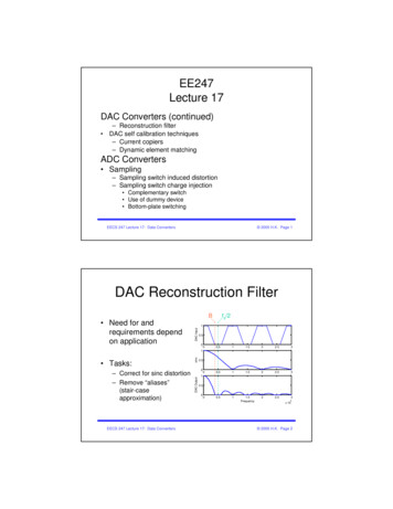
EE247Lecture 17DAC Converters (continued) – Reconstruction filterDAC self calibration techniques– Current copiers– Dynamic element matchingADC Converters Sampling– Sampling switch induced distortion– Sampling switch charge injection Complementary switch Use of dummy device Bottom-plate switchingEECS 247 Lecture 17: Data Converters 2005 H.K. Page 1DAC Reconstruction FilterBfs/21DAC Input Need for andrequirements dependon application0.5000.511.522.5– Correct for sinc distortion– Remove “aliases”(stair-caseapproximation)EECS 247 Lecture 17: Data Converterssincx 100.50DAC Output Tasks:36100.511.522.5361x 100.5000.511.5Frequency22.536x 10 2005 H.K. Page 2
Reconstruction Filter OptionsD igitalF ilterDACSCFilterCTF ilterZOH Digital and SC filter possible only in combination withoversampling (signal bandwidth B fs/2) Digital filter– Band limits the input signal à prevent aliasing– Could also provide high-frequency pre-emphasis tocompensate in-band sinc amplitude droop associated withthe inherent DAC ZOH functionEECS 247 Lecture 17: Data Converters 2005 H.K. Page 3DAC Implementation Examples Untrimmed segmented– T. Miki et al, “An 80-MHz 8-bit CMOS D/A Converter,” JSSCDecember 1986, pp. 983– A. Van den Bosch et al, “A 1-GSample/s Nyquist Current-SteeringCMOS D/A Converter,” JSSC March 2001, pp. 315 Current copiers:– D. W. J. Groeneveld et al, “A Self-Calibration Technique forMonolithic High-Resolution D/A Converters,” JSSC December1989, pp. 1517 Dynamic element matching:– R. J. van de Plassche, “Dynamic Element Matching for HighAccuracy Monolithic D/A Converters,” JSSC December 1976, pp.795EECS 247 Lecture 17: Data Converters 2005 H.K. Page 4
8x8 arrayEECS 247 Lecture 17: Data Converters2µ tech., 5VsupplySegmented (6 2) 2005 H.K. Page 5Two sources of systematic error:- Finite current source output resistance- Voltage drop due to finite ground bus resistanceEECS 247 Lecture 17: Data Converters 2005 H.K. Page 6
Current-Switched DACs in CMOSI1 k (VGSM 1 Vth )VGSM 2 VGSM 1 4RI, VGSM 3 VGSM 1 7RIVG SM 4 VG SM 1 9RI, VG SM 5 VGSM 1 10RI24RI 2I 2 k (VGSM 2 Vth ) I1 1 VGSM 1 Vth 2I1gmM 1 VGSM 1 Vth2IoutVDDM1M2I1I2M3I3M4I4 M 5 I52 4RgmM 1 I 2 I1 1 I1 (1 4RgmM 1 ) 2 2 7RgmM 1 I 3 I1 1 I1 (1 7RgmM 1 ) 2 2 9RgmM 1 I 4 I1 1 I1 (1 9RgmM 1 ) 2 2 10RgmM 1 I 5 I1 1 I1 (1 10RgmM 1 ) 2Rx4IRx3IRx2IRxIExample: 5 unit element current sources Assumption: RI is small compared to transistor gate overdriveà Desirable to have gm smallEECS 247 Lecture 17: Data Converters 2005 H.K. Page 7Current-Switched DACs in CMOSExample: INL of 7 unit element DACINL [LSB]0.3Sequential current source switchingSymmetrical current source switching0.20.10-0.101234Input567Example: 7 unit element current source DAC- assume gmxR 1/100 If switching of current sources sequential (1-2-3-4-5-6-7)à INL 0.25LSB If switching of current sources symmetrical (4-3-5-2-6-7 )à INL 0.09, -0.058LSBEECS 247 Lecture 17: Data Converters 2005 H.K. Page 8
Current-Switched DACs in CMOSExample: DNL of 7 unit element DACDNL [LSB]0.20.10-0.1-0.2Sequential current source switchingSymmetrical current source switching1234567InputExample: 7 unit element current source DAC- assume gmxR 1/100 If switching of current sources sequential (1-2-3-4-5-6-7)à DNLmax 0.15LSB If switching of current sources symmetrical (4-3-5-2-6-7 )à DNL 0.15LSBEECS 247 Lecture 17: Data Converters 2005 H.K. Page 9(5 5)More recent published DAC using symmetrical switching built in 0.35µ/3Vanalog/1.9V digital, area x10 smaller compared to previous exampleEECS 247 Lecture 17: Data Converters 2005 H.K. Page 10
EECS 247 Lecture 17: Data Converters 2005 H.K. Page 1116bit DAC (6 10)- MSB DAC uses calibrated current sourcesI/2CurrentDividerEECS 247 Lecture 17: Data ConvertersI/2I 2005 H.K. Page 12
EECS 247 Lecture 17: Data Converters 2005 H.K. Page 13Current Divider AccuracyId d IdIdd IdId I d1 I d 22I d1 I d 2I/2I/2M1M2II/2 dId /2M1I/2-dId /2M2IId d W L d Vth VG S Vt h W L 2Ideal CurrentDividerReal CurrentDividerM1& M2 mismatchedàProblem: Device mismatch could severely limit DAC accuracyEECS 247 Lecture 17: Data Converters 2005 H.K. Page 14
EECS 247 Lecture 17: Data Converters 2005 H.K. Page 15Dynamic Element MatchingDuring Φ2During Φ1I1(1) 21 Io (1 1 )I2(1) 21 Io (1 1 )I1( 2 ) 21 Io (1 1 )Io/2I2( 2 ) 21 Io (1 1 )Io/2I1I2fclkI (1) I2( 2 )I2 22I (1 1 ) (1 1 ) o22Io f o r 1 s m a l l2EECS 247 Lecture 17: Data Converters/ 2 error 1Io 2005 H.K. Page 16
EECS 247 Lecture 17: Data Converters 2005 H.K. Page 17Dynamic Element MatchingDuring Φ2During Φ1I1(1) 12 I o (1 1 )I(1)2 I o (1 1 )12I 3(1) 12 I1(1) (1 2 ) I o (1 1 )(1 2 )I1( 2 ) 12 I o (1 1 )I( 2)2 I o (1 1 )12I 3( 2 ) 12 I1( 2 ) (1 2 )14 14 I o (1 1 )(1 2 )I 3(1) I 3( 2 )2I (1 1 )(1 2 ) (1 1 )(1 2 ) o42I o (1 1 2 )4Io/4Io/2Io/4I3I4I2fclk/ 2 error 2I1I3 E.g. 1 2 1% à matching error is (1%)2 0.01%EECS 247 Lecture 17: Data Convertersfclk/ 2 error 1Io 2005 H.K. Page 18
SummaryD/A Converter D/A architecture– Unit element – complexity proportional to 2B- excellent DNL– Binary weighted- complexity proportional to B- poor DNL– Segmented- unit element MSB(B1) binary weighted LSB(B2)à complexityproportional (2B1-1) B2 – DNL compromise between the two Static performance Dynamic performance DAC improvement techniques– Component matching– Glitches– Symmetrical DAC element switching rather than sequential switching– Current source self calibration– Dynamic element matchingEECS 247 Lecture 17: Data Converters 2005 H.K. Page 19MOS Sampling CircuitsEECS 247 Lecture 17: Data Converters 2005 H.K. Page 20
Re-CapAnalog InputAnti-AliasingFilterAnalogPreprocessing How can webuild circuitsthat "sample"Sampling on"Bits toStaircase"AnalogPost processingReconstructionFilterAnalog OutputEECS 247 Lecture 17: Data Converters 2005 H.K. Page 21Ideal Samplingφ1 In an ideal world,zero resistancesampling switcheswould close for thebriefest instant tosample a continuousvoltage vIN onto thecapacitor C Not realizable!EECS 247 Lecture 17: Data ConvertersvINvOUTS1Cφ1T 1/fS 2005 H.K. Page 22
Ideal T/H Samplingφ1vINvOUTS1Cφ1T 1/fS Vout tracks input when switch is closed Grab exact value of Vin when switch opens "Track and Hold" (T/H) (often called Sample & Hold!)EECS 247 Lecture 17: Data Converters 2005 H.K. Page 23Ideal T/H SamplingContinuousTimetimeT/H signal(SD Signal)ClockDT SignalEECS 247 Lecture 17: Data Converters 2005 H.K. Page 24
Practical Samplingφ1vINvOUTM1C Switch induced noise power à kT/CFinite Rsw à limited bandwidthRsw f(Vin) à distortionSwitch charge injectionClock jitterEECS 247 Lecture 17: Data Converters 2005 H.K. Page 25kT/C Noisek BT 2 12C 2B 1 C 12k BT VFS 2In high resolution ADCs kT/C noise usually dominatesoverall error (power dissipation considerations).BCmin (VFS 1V)8121416200.003 pF0.8 pF13 pF206 pF52,800 pFEECS 247 Lecture 17: Data Converters 2005 H.K. Page 26
Acquisition Bandwidth The resistance R ofswitch S1 turns thesampling network into alowpass filter withrisetime RC τφ1vINvOUTR S1C Assuming Vin isconstant during thesampling period and Cis initially dischargedvout (t ) vin (1 e t /τ )EECS 247 Lecture 17: Data Converters 2005 H.K. Page 27Switch On-Resistance 1 Vin Vout t 2fs 1Vin e2 f sτ Vin VFSWorst Case:τ R φ1vINC1T2 ln 2 B 1()112 f sC ln 2 B 1Example:B 14,(vOUTR S1)C 13pF, fs 100MHzφ1T 1/fST/τ 19.4, R 40ΩEECS 247 Lecture 17: Data Converters 2005 H.K. Page 28
Switch On-ResistanceI D ( triode ) µCoxRON µCoxforRON WLVDS VGS VTH 2 VDS , dI D ( triode )1 RONdVDSVDS 011 WW(VGS Vth ) µCox (VDD Vth Vin )LLRo 1WµCox (VDD Vth )LRoVin1 VDD VthEECS 247 Lecture 17: Data Converters 2005 H.K. Page 29Sampling Distortionvout T Vin 1 2τ VDD Vt h vi n 1 e 10bit ADC & T/τ 10VDD – Vth 2VVFS 1VEECS 247 Lecture 17: Data Converters 2005 H.K. Page 30
Sampling Distortion SFDR is very sensitive tosampling distortion Solutions: Overdesignà Largerswitchesà increased switchcharge injectionà increased switchdrain & source C Complementary switch Maximize VDD/VFSà decreased dynamicrange Constant VGS ? f(Vin)à 10bit ADC T/τ 20VDD – Vth 2VVFS 1VEECS 247 Lecture 17: Data Converters 2005 H.K. Page 31Practical Samplingφ1 kT/C noise 2B 1 C 12k BT VFS 2vINvOUTM1C Finite Rsw à limited bandwidthR 112 f sC ln 2 B 1() gsw f(Vin) à distortionVin gON g o 1 for VDD Vth g o µ CoxW(VDD Vth )L Switch charge injection Clock jitterEECS 247 Lecture 17: Data Converters 2005 H.K. Page 32
Sampling DistortionEffect of Supply Voltage10bit ADC & T/τ 10VDD – Vth 2VVFS 1V10bit ADC & T/τ 10VDD – Vth 4VVFS 1V Effect of lower supply voltage on sampling distortionà HD3 increases by (VDD1/VDD2)2à HD2 increases by (VDD1/VDD2)EECS 247 Lecture 17: Data Converters 2005 H.K. Page 33Sampling Distortion SFDR à sensitive tosampling distortion improve linearity by: Larger VDD Higher sampling bandwidth Solutions: Overdesignà Largerswitchesà Increased switchcharge injectionà Increased nonlinear S&D junction cap. Maximize VDD/VFSàDecreased dynamic rangeif VDD const. Complementary switch Constant & max. VGS ? f(Vin)EECS 247 Lecture 17: Data Converters10bit ADC T/τ 20VDD – Vth 2VVFS 1V 2005 H.K. Page 34
Complementary Switchφ1goφ1Bg ongoT gon gopg opφ1φ1B Complementary n & p switch advantages: Increases the overall conductance Linearize the switch conductance for the rangeVtp Vin Vdd-VtnEECS 247 Lecture 17: Data Converters 2005 H.K. Page 35Complementary Switch IssuesSupply Voltage Evolution Supply voltage scales down with technology scaling Threshold voltages do not scale accordinglyRef: A. Abo et al, “A 1.5-V, 10-bit, 14.3-MS/s CMOS Pipeline Analog-to-Digital Converter,” JSSCMay 1999, pp. 599.EECS 247 Lecture 17: Data Converters 2005 H.K. Page 36
Complementary SwitchEffect of Supply Voltage Scalinggogonφ1goT gon gopgopφ1Bφ1φ1B As supply voltage scales down input voltage range for constant go shrinksà Complementary switch not effective when VDD becomes comparable to VthEECS 247 Lecture 17: Data Converters 2005 H.K. Page 37Boosted & Constant VGS SamplingVGS const. Increase gate overdrive voltage as much as possible keep VGSconstantØ Switch overdrive voltage is independent of signal levelØ Error from finite RON is linear (to first order)Ø Lower Ron achieved à lower time constantEECS 247 Lecture 17: Data Converters 2005 H.K. Page 38
Constant VGS Sampling( voltage @ the switch source terminal)EECS 247 Lecture 17: Data Converters 2005 H.K. Page 39P NConstant VGS Sampling CircuitVDD 3VM2M1M3M8M6M4PP mpling switch & CThis Example: All device sizes:10µ/0.35µAll capacitor size: 1pFEECS 247 Lecture 17: Data Converters 2005 H.K. Page 40
Clock Voltage Doubler2VDDVDD 3VM2M1R1P BoostR2VDDC2C1P NP0VP1Clock period: 100ns*R1 & R2 1GOhmà dummy resistors added for simulation onlyEECS 247 Lecture 17: Data Converters 2005 H.K. Page 41Constant VGS Sampler: Φ LOWVDD 3VM3 2 VDD(boosted clock)VDDOFF Sampling switch M11is OFFM4C3DeviceOFFVDDM12OFFM11OFFVS11.5V1MHzInput voltagesourceEECS 247 Lecture 17: Data ConvertersChold1pF C3 charged to VDD 2005 H.K. Page 42
Constant VGS Sampler: Φ HIGHConstant Vgs Switch:P is HIGH C3 previouslycharged to VDDM8VDDC31pF M8 & M9 are on:C3 across G-S of M11M11M9VS11.5V1MHzEECS 247 Lecture 17: Data ConvertersChold1pF M11 on with constantVGS VDD 2005 H.K. Page 43Constant VGS SamplingInput Switch VGateChold SignalInput SignalEECS 247 Lecture 17: Data Converters 2005 H.K. Page 44
Complete CircuitClock MultiplierM7 & M13 forreliabilitySwitchRef: A. Abo et al, “A 1.5-V, 10-bit, 14.3-MS/s CMOS Pipeline Analog-to-DigitalConverter,” JSSC May 1999, pp. 599.EECS 247 Lecture 17: Data Converters 2005 H.K. Page 45Advanced Clock BoostingRef: H. Pan et al., "A 3.3-V 12-b 50-MS/s A/D converter in 0.6um CMOS with over 80-dBSFDR," IEEE J. Solid-State Circuits, pp. 1769-1780, Dec. 2000]EECS 247 Lecture 17: Data Converters 2005 H.K. Page 46
Advanced Clock Boosting TechniqueRef: M. Waltari et al., "Aself-calibrated pipelineADC with 200MHz IFsampling frontend,"ISSCC 2002, Dig.Techn. Papers, pp.314SamplingSwitch Gate tracks average of input and output, reduces effect of I·Rdrop at high frequencies Bulk also tracks signal reduced body effect (technology usedallows connecting bulk to S) SFDR 76.5dB at fin 200MHz (measured)EECS 247 Lecture 17: Data Converters 2005 H.K. Page 47Switch Off-Mode Feedthrough CancellationRef: M. Waltari et al., "A self-calibrated pipeline ADC with 200MHz IF-sampling frontend,"ISSCC 2002, Dig. Techn. Papers, pp. 314EECS 247 Lecture 17: Data Converters 2005 H.K. Page 48
Practical Samplingφ1vINvOUTM1C Rsw f(Vin) à distortion Switch charge injectionEECS 247 Lecture 17: Data Converters 2005 H.K. Page 49Sampling Switch Charge InjectionVGVGVHVIN VthVINVINVLCstVOVOM1 VVINtofft First assume VIN is a DC voltage When switch turns off à offset voltage induced on Cs Why?EECS 247 Lecture 17: Data Converters 2005 H.K. Page 50
SamplingSwitch Charge InjectionCross section viewDistributed channel resistance &gate & junction capacitancesLDCovMOS xtor operating in triode regionGLCovSDB Channel à distributed RC network Channel to substrate junction capacitance à distributed & variable Over-lap capacitance Cov LDxWxCox associated with GS & GD overlapEECS 247 Lecture 17: Data Converters 2005 H.K. Page 51Switch Charge InjectionSlow ClockVGVHVIN VthVINVLVOVINt Vt- tofft Since clock fall time device speedà During the period (t- to toff) current in channel discharges channel chargeinto low impedance signal source Only source of error à Charge transfer from Cov into CsEECS 247 Lecture 17: Data Converters 2005 H.K. Page 52
Switch Charge InjectionSlow ClockVGVGVHCovVIN VthVINDCsVLtVO V CovCo v Cs(Vi Vt h VL )Co v(Vi Vth VL )CsVo Vi (1 ε ) Vos where ε VVINCo vCs; Vo s Co vCst- tofft(Vth VL )EECS 247 Lecture 17: Data Converters 2005 H.K. Page 53Switch Charge InjectionSlow Clock- ExampleVG12µ/0.35µVINM1VGVOVHCs 1pFVINVIN VthVLtVOC' ov 0 . 3 fF / µ Co x 5 fF / µ 2 Vth 0.5Vε CovVos CovCsCs 12µ x0 . 3 fF / µ1pF VVIN .36% 7 bit(Vth VL ) 1.8mVEECS 247 Lecture 17: Data Converterst- tofft 2005 H.K. Page 54
Switch Charge InjectionFast ClockVGVGM1VINVHVIN VthVOVINCs 1pFVLtVO VVINtofft Sudden gate voltage drop à no gate voltage to establish current in channel àchannel charge has no choice but to escape out towards S & DEECS 247 Lecture 17: Data Converters 2005 H.K. Page 55Switch Charge InjectionFast ClockVG Vo Co vCo v CsCovCov Cs(VH VL ) 12 Qc h1 WCo x ( L 2LD ) ( (VH Vi Vth ))(VH VL ) 2CsCsVINVLtVO1 WCox Lwhere ε 2CsCo vVIN VthCsVo Vi (1 ε ) VosVos VH VVIN1 W Cox L (VH Vt h )(VH VL ) 2Cstoff Assumption à channel charge divided equally between S & D Source of error à channel charge transfer charge transfer from Cov into CsEECS 247 Lecture 17: Data Converters 2005 H.K. Page 56t
Switch Charge InjectionFast Clock- ExampleVGVG12µ/0.35µVHVINVIN VthVOM1VINCs 1pFVLtVO VVINCov 0.3 f F / µ Cox 5 f F / µ 2 Vth 0 . 5V VD D 3Vε 1/ 2WLCoxCs 12µ x0.35x5 f F / µ1pF 2.1% 4.5 bittofft1 WC L (V V )Vos (VH VL ) ox H th 9mV 26.3mV 45.3mVCs2CsCo vEECS 247 Lecture 17: Data Converters 2005 H.K. Page 57Switch Charge InjectionExampleεVOS45mV2.1%1.8mV.36%Clock fall timeClock fall timeà Both errors are a function of clock fall time, input voltage level, source impedance& sampling capacitanceEECS 247 Lecture 17: Data Converters 2005 H.K. Page 58
Switch Charge InjectionError Reduction How do we reduce the error?àReduce switch?τ RON Cs Vo CsµCox1 Qc hL(VG S Vth )2 CsFOM τ Vo FOM WCsµCo xWL1 WCox L ( (VH Vi Vt h ) ) (VGS Vt h ) 2CsL2µàReducing switch size increases τ à increased distortionà not a viable solutionàSmall τ and V à use minimum chanel lengthàFor a given technology τ x V conts.EECS 247 Lecture 17: Data Converters 2005 H.K. Page 59Sampling Switch Charge InjectionSummary Extra charge injected onto sampling capacitor @switch device turn-off– Charge sharing with Cov– Channel charge transfer Issues:– DC offset– Input dependant error voltage à distortion Solutions:– Complementary switch?– Addition of dummy switches?– Bottom-plate sampling?EECS 247 Lecture 17: Data Converters 2005 H.K. Page 60
Switch Charge InjectionComplementary Switchφ1VGVHVINφ1BVLtφ1φ1B In slow clock case if area of devices are equal à effect of overlap capacitor for n& p devices cancel to first order (matching n & p area)EECS 247 Lecture 17: Data Converters 2005 H.K. Page 61Switch Charge InjectionComplementary SwitchFast ClockQc h n WnCox Ln (VH Vi Vth n )Qch p WpCo x Lp (Vi V L Vt h p ) 1 QQ Vo c h p ch n 2 CsCs Vo Vi (1 ε ) Vo s1 W C L WpCox Lpε n ox n2Cs In fast clock case§Offset cancelled for equal device area§Input voltage dependant error worse!EECS 247 Lecture 17: Data ConvertersVGVHVINVLtφ1φ1B 2005 H.K. Page 62
Switch Charge InjectionDummy SwitchVGVGBWM2 1/2WM1VINM1VHVOM2VGVGBVINCsVLt Dummy switch same L as main switch but half W Main device clock goes low, dummy device goes high à dummy switch acquiressame amount of channel charge main switch needs to lose§ Effective only if exactly half of the charge transferred to M2 and good matchingbetween clock fall/riseEECS 247 Lecture 17: Data Converters 2005 H.K. Page 63Switch Charge InjectionDummy SwitchVINVGVGB W 1/2WM1M2M1M2RCsVOCs§ To guarantee half of charge goes to each sideà create the sameenvironment on both sidesv Add C equal to sampling capacitor to the other side of the switch add fixed resistor§ Degrades sampling bandwidthEECS 247 Lecture 17: Data Converters 2005 H.K. Page 64
Dummy SwitchDummy Switch Effectiveness Test Dummy switchà W 1/2W main Note large Lsà good devicearea matchingRef: L. A. BIENSTMAN et al, “ An Eight-Channel 8 13it Microprocessor Compatible NMOS D/AConverter with Programmable Scaling”, IEEE JSSC, VOL. SC-15, NO. 6, DECEMBER 1980EECS 247 Lecture 17: Data Converters 2005 H.K. Page 65Switch Charge InjectionBottom Plate Samplingφ1aφ1bVHM1AVO VI CsVLφ1bM2AVOVI-M1BCsφ1aM2BEECS 247 Lecture 17: Data Converterst Switches M2A@ B are opened slightly earliercompared to M1A&Bà Injected charge by the opening of M2ABis constant & eliminated when useddifferentially Since bottom plate of Cs is open when M1A&Bare openedà no charge injected on Cs 2005 H.K. Page 66
Divider Current Divider Accuracy I I/2 dI d /2 Real Current Divider M1& M2 mismatched d1d2 d dd1d2 dd W d L th W dGSth L II I 2 dIII II dI2d dV IVV . Switch induced noise power àkT/C Finite R sw àlimited bandwidth R sw f(V in) àdistortion Switch charge injection Clock jitter