Transcription
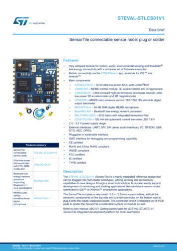
AN5235Application noteSTEVAL-IPFC01V1 3 kW three channel interleaved PFC with STNRGPF01 digitalcontrollerIntroductionThe STEVAL-IPFC01V1 is a 3 kW interleaved PFC evaluation board for the STNRGPF01 digital configurable IC, which is ableto drive up to three channels in an interleaved PFC for industrial applications.The evaluation board achieves high power density (52 W/inch3), thanks to a compact layout with small magnetic components,which is possible because of the interleaving effect and chosen switching frequency.Moreover, the PFC is used to satisfy the IEC 61000-3-2 standard for electrical equipment.Figure 1. STEVAL-IPFC01V1 reference designThe STNRGPF01 controller is embedded on a separate control board and implements mixed signal (analog/digital) averagecurrent mode control in CCM at a fixed frequency. The analog section ensures cycle by cycle current regulation, while digitalcontrol manages the non-time critical operations, providing further flexibility.The device can be customized for different applications by using a dedicated software tool.RELATED LINKSVisit the STNRGPF01 web folder on www.st.com for all the available data and information regarding the deviceAN5235 - Rev 2 - September 2019For further information contact your local STMicroelectronics sales office.www.st.com
AN5235Safety instructions1Safety instructionsDanger:The evaluation board uses voltage levels that can cause serious injury and even death.Do not touch any of the boards immediately after disconnecting the input power supply as thecharged capacitors need time to discharge.Due to the high power density, the board components and the heat sink can become very hot andcause severe burns when touched.This board is intended for use by skilled technical personnel who are suitably qualified and familiar with theinstallation, use and maintenance of power electronic systems. The same personnel must be aware of and mustapply national accident prevention rules.The electrical installation shall be completed in accordance with the appropriate requirements (e.g., crosssectional areas of conductors, fusing, and GND connections).AN5235 - Rev 2page 2/54
AN5235Functional overview2Functional overviewFigure 2. STEVAL-IPFC01V1 block diagram1. I/O measurement signals2. Analog circuitry3. Power stage4. Digital control sectionACinput3EMI filter&rectificationPWM01Itot ngularwavegenerator13Driver4PWM0flip-flopSET1 RESET13LoadPWM23Driver3Analog 2filterSIN lySET2 RESET2OUT PI[2],[3]VDDTRIANG REFVSS4CLOCKSTNRGPF01VINIOUTVOUT11When an AC input voltage in the appropriate range is supplied, the DC output voltage increases up to the peakvalue of the line input voltage and the auxiliary power supply starts supplying voltages for the STNRGPF01 anddrivers.I/O measurement signals are used to: Verify starting and operating conditions (for example, 50/60 Hz, load/no-load start-up etc.) Regulate DC output voltage Generate feed-forward compensation, phase shedding and current balance functions Trigger cooling system and safety shut-down (for example, due to over or undervoltage conditions)The STNRGPF01 outputs a sinusoidal current reference (SIN REF) for the input current regulation performed byanalog circuitry, which provides the signals (TRIANG REF, OUT PI[2],[3]) for triangular-carrier PWM modulation.The master PWM signal (PWM0) directly drives the first channel, while two external flip-flops receive the set andreset signals from the STNRGPF01 controller and generate the interleaved PWM signals for the other channels(PWM1, PWM2).The status LEDs indicate the following conditions: Green LED: PFC OK, start-up has completed Red LED: PFC FAULT, a fault has occurredCertain STNRGPF01 functions and parameters are configurable through the eDesign Suite tool.RELATED LINKS7 PFC controller customization with eDesign Suite on page 31AN5235 - Rev 2page 3/54
AN5235Power factor correction3Power factor correctionIn many applications, ranging from telecom to common industrial power supplies (SMPS), active Power FactorCorrector (PFC) converters are used as the first stage in AC/DC conversion to draw a sinusoidal-shape inputcurrent in phase with grid voltage.PFCs allow any downstream electrical appliance to appear as a purely resistive load, and improve the overall gridefficiency.3.1Power factor (PF) - definitionThe total power absorbed by a load connected to the grid is known as apparent power, which includes twocomponents:1.Real power: the power that actually produces work (e.g., motion, heating) in a system.2.Reactive power: required by inductive loads for normal operation.The ratio between real power and apparent power is known as power factor (PF):PF In a real system, the PF can be calculated as:realpowerapparentpowerPF displacementfactor distortionfactor (1)cosϕ(2)1 THD2where:cos ϕ displacement factor: the phase shift between input current and line voltage. 11 THD2 distortion factor: the PF degradation due to the harmonic component of input current.The total harmonic distortion (THD) takes into account the amplitude of input current harmonics with respect tothe fundamental component:Ii 2nTHD i 2I1(3)Where:I1 input current at fundamental frequency Ii ith harmonic of input currentThe ideal condition is to have a displacement factor of one and a THD as low as possible, so the apparent poweris minimized and the size and cost of generators and transmission lines can be reduced.3.2Active PFCAs boost circuits are relatively straightforward to design and drive, they are the preferred topology forimplementing PFC’s.The boost PFC pre-regulator receives input from the bridge rectifier and delivers a constant DC output voltage(higher than the peak line voltage), while shaping input current at twice the line frequency.A second conversion stage provides the appropriate voltage for a generic DC or AC load.AN5235 - Rev 2page 4/54
AN5235Active PFCFigure 3. PFC boost circuit and ideal waveformsvINvACiLLvLiDDiOUTiCiSCiACPFC ControllerS DC/DCorDC/ACvOUTvACLoadBoost PFC Pre-RegulatorPFC waveforms at switching frequencyPFC waveforms at line frequencyvAC,iACvLvINS 1tS 0vIN -vOUTtiS,iDvIN,iLiLtTLINE /2TONvOUTTOFFiLTLINEtvINLtvIN -vOUTLTSWtAs shown in the above figure, the switching period (Tsw) can be divided into the following intervals:TON during which the inductor current increases linearly through a switch (S 1).1.2.TOFF after the switch is closed (S 0) and the inductor current flows through the boost diode towards theload.The following operation modes are defined according to the level which the inductor current drops during TOFF:1.2.3.Continuous Conduction Mode (CCM)Discontinuous Conduction Mode (DCM)Critical Conduction Mode (CrM)Table 1. Boost operation modesInductor current waveformOperation ModeContinuous Conduction Mode (CCM)Discontinuous Conduction Mode (DCM)AN5235 - Rev 2Features Always hard-switching Inductor value is largest Minimal rms current Highest rms current Reduce coil inductance Best stabilitypage 5/54
AN5235Active PFCInductor current waveformOperation ModeFeaturesCritical Conduction Mode (CrM) Largest rms current Switching frequency is not fixedCCM is the preferred mode for high power PFC converters because it offers advantages like low input peakcurrent (low turn-off switching losses), low input current THD and high power factor.CCM generates high turn-on switching losses (hard switching), however, which is why parallel solutions are oftenpreferable.3.2.1InterleavingInterleaving consists of paralleling two or more small stages (channels) instead of one larger channel. Theadvantages of interleaving come at the expense of circuit simplicity, so this architecture is usually reserved forhigh power applications, above 600 W.Figure 4. Interleaved boost circuit N-channelvINL1D1L2D2LNDNPFC ControllerS1S2C vOUTSNDuring normal operation, the PWM driving signals are out of phase by the following amount:pℎasesℎift 360 numberofcℎannels(4)The total power is shared among the parallel circuits.The interleaved topology has the following advantages over a traditional single-stage PFC: Input current ripple reduction EMI filter volume reduction Inductor volume reduction Output capacitor RMS current value reduction Better power management for the switches higher efficiency thanks to channel power managementThrough interleaving, the equivalent inductor current ripple is reduced and completely eliminated for certain dutycycle values (e.g., at D 0.5 for two-channel boost; D 0.33 and D 0.66 for 3-channel PFC).The EMI filter size can therefore be reduced thanks to the higher equivalent switching frequency.AN5235 - Rev 2page 6/54
AN5235Active PFCFigure 5. Channel inductor currents vs total current for 3-channel PFCThe following diagram shows the difference in inductor size for a single channel PFC with respect to a 3-channelinterleaved solution. The 3-channel solution occupies over 40% less volume.Figure 6. Inductor volume comparison for 3 kW PFCSwitching frequency 100 KHz1. Single channel: Core EE70, L 150µH, size 70x66x31mm, volume 143cm32. Interleaved 3 channels: Core PQ3230, L 120µH, size 30x32x27mm, volume 26cm3 (x3)Interleaving also allows a lower switching frequency than a single-channel PFC for the same power rating, whichalso helps improve efficiency. Moreover, the inductor current ripple reduction produces a reduced RMS outputcapacitor current, so capacitors with higher ESR (lower cost) can be used.AN5235 - Rev 2page 7/54
AN5235Mixed signal approachFigure 7. Output capacitor current ripple vs duty cycle1. Single channel2. Two channels3. Three channelsConverter efficiency can also be improved by enabling or disabling the parallel channels depending on loadpercentage (phase shedding).Even if interleaving leads to an increase in the number of switches, they are still smaller and less costly becausethe switches only manage a portion of total power. Interleaving also allows the distribution of power dissipationmore evenly over the channels.3.3Mixed signal approachProgrammable digital solutions can provide adequate regulation across the entire input and output range of apower supply, which analog ICs alone often cannot deliver. Fully digital solutions, however, require highperformance microcontrollers able to manage the high bandwidth of the current control loop.A good compromise is mixed signal control, where: The current loop is managed by a hardware analog compensator, ensuring cycle by cycle regulation. The voltage loop is managed by a relatively low-cost digital controller, which provides output voltageregulation and non-time critical functions such as multiplier, feed-forward compensation, and undervoltage orovervoltage protection on the input and output voltages.AN5235 - Rev 2page 8/54
AN5235Mixed signal approachFigure 8. Mixed signal block diagramVinBridgeRectifierPFCVoutLOADPWMAnalog CurrentCompensatorduty cyclewaveIref- IinTriangularwaveDACorAnalog filterVinDigital VoltagecontrolVoutVout refFor lower end controllers that do not include a DAC, the current reference can be generated through a PWMwaveform, which is then filtered to become the sinusoidal reference (Iref) for the current loop.AN5235 - Rev 2page 9/54
AN5235PFC control4PFC controlThe STNRGPF01 three-channel interleaved CCM PFC digital controller offers the advantages of a very high enddigital solution without the typical limits of analog controllers.The STNRGPF01 can drive a PFC in CCM at a fixed frequency, using mixed signal (analog/digital) AverageCurrent Mode control (ACM) to deliver lower inductor ripple current, less EMI filtering, reduced RMS input currentand operation at high power levels.The following figure shows cascaded control of voltage and current loops, which determines the output voltage byregulating the total average inductor current.Figure 9. STNRGPF01 mixed signal block schemeThis type of control is designed for fast transient responses to avoid large over and under-shoots on the outputvoltage when the mains voltage changes suddenly or a load current step occurs.The system works in the following way:1.The difference between output voltage feedback vout fb and reference vout ref is sent to a digital PI, whichcalculates the peak total input average current ipk ref.2.AN5235 - Rev 2The PFC current reference is internally generated and exits the I/O FFD block as a PWM waveform; afterfiltering it becomes the total average sinusoidal input current reference itot ref for the inner current loop(analog section, red dashed line).page 10/54
AN5235Converter modeling3.4.4.1The difference between current reference itot ref and input current feedback itot fb is sent to an analog PI; themaster PWM signal is generated by comparing the analog PI output vctrl and a triangular wave vtriang atswitching frequency.Finally, interleaving produces three 120 phase shifted PWM signals (180 for two channels) to drive thethree power switches.Converter modelingThe interleaved boost converter small-signal transfer functions are obtained through the following operations:1.State-space averaging (SSA), used to average the converter behavior over a switching period, so theresulting small-signal model is only valid if the control loop bandwidth is suitably lower than the switchingfrequency.2.Linearization with Taylor’s series around an operating point.The small-signal transfer functions are useful to calculate the PI regulator parameters and satisfy bandwidth andphase margin specifications for control loops.For the sake of simplicity, we shall assume that: The converter operates in CCM mode only. Active and passive components are ideal. The parallel boost inductors are identical and the total power is shared symmetrically across the channels. Perturbations on the main voltage are neglected and the voltage is assumed to be constant across severalswitching cycles.4.2Current loop designFigure 10. Current loop block diagramNote:In the following equations, the tilde ( ) symbol above a letter indicates a small-signal variable, while uppercaseletters refer to steady-state operating point variables.The control-to-input current transfer function is:ĩtotGi s ̃ δ13 s PCOUTVOUTOUT 1 η VOUT2 s2 L2COUTLPFCVOUTPFCPOUTs NcℎVIN(5)Where: ĩtot small-signal total input average inductor current AN5235 - Rev 2ĩtot ref small-signal total input average current referenceĩtot fb small-signal total input average inductor current sensingẽ i small-signal current errorṽ ctrl small-signal control voltage (analog PI out)δ̃ small-signal duty cycleVpk triang peak-to-peak voltage of triangular wave (carrier at switching frequency)KPI out scale factor used to match PI maximum out voltage and Vpk triang (resistive divider)VIN rms input voltageVOUT rms output voltagePOUT output powerpage 11/54
AN5235Current loop designNcℎ number of channels LPFC single channel boost inductor COUT output capacitor η estimated efficiency Ai Input current sensing gain Ci s Input current compensator transfer function While this formula suggests that Gi s depends on the number of channels and operating input voltage, thefollowing figures show that they do not affect the Bode diagram behavior at high frequencies (current loopcrossover frequency).Figure 11. Control-to-input current TF vs main voltage VIN (rms)Magnitude (dB)VIN 90VGi(s) vs V IN80VIN 115VVIN 140V60VIN 185VVIN 230V40VIN 265V200-2090Phase (deg)450-45-90-135-110100101102103104Frequency (Hz)AN5235 - Rev 2page 12/54
AN5235Current loop designFigure 12. Control-to-input current TF vs Number of active channels NchGi(s) vs N chMagnitude (dB)80Nch 160Nch 240Nch 3200-2090Phase (deg)450-45-90-135-110100101102103104Frequency (Hz)so Gi s can be simplified as:ĩtotVOUTGi s ̃ sLPFCδ(6)The typical PI compensator transfer function is:Ci s KP Itots KI Itots(7)KI Itotwith one pole at zero frequency pi 0 to reset the steady-state error and one zero zi Kto achieve theP Itotdesired phase margin at crossover frequency of the following open loop transfer function:Ti s Ci s Li sWhere: KPI out(8)Li s VAiGi spk triangBased on general Bode criteria, the following equations ensure system stability for a desired bandwidth ωTi des(crossover pulsation) and phase margin PMi desTi jωTi des 1 Ti jωTi des 180 PMi desCurrent loop crossover frequency fTi des Where: fline line voltage frequency ωTi desmust be selected in the range:2πfswfline fTi des 2(9)(10)fsw switching frequencyThis relationship is necessary for good input current regulation and switching noise immunity. Crossoverfrequency and phase margin for current loop are typically selected as:AN5235 - Rev 2page 13/54
AN5235Current loop designfTi 2 10kHzdesPMi 45 60 des(11)So the compensator parameters are calculated by:KI Itot Li jωTi desωTi des1 tan2 PMi des 90 Li jωTi des(12)KI Itottan PMi des 90 Li jωTi desKP Itot ωTi desAs the current loop is performed in hardware, a PI Type II OP-AMP compensator is used:Figure 13. PI Type II OP-AMP compensatorThe transfer function is:Ci opamp s the locations of the poles and zero are:fpi0 0 Cfz Cfp1Cfz Cfp RiCfzRfs 1CfzCfpRfss 1Cfz Cfp(13)1fpi1 2πC C R 2πC Rfz fp ffp f1fzi1 2πC Rfz fComparing Eq. (7) with Eq. (13), an additional high-frequency pole appears in Eq. (13). It is given by capacitorCfp and is usually set at half the switching frequency to attenuate switching noise without interfering with currentloop regulation:Cfp Cfzfsw fpi1 fsw2(14)Proportional and integral gain of the compensator determines the passive network design:1Ri CfzKI ItotRf RiKP Itot(15)fsw1 Cfp fπfswRf pi12As we need to calculate four components from three equations, capacitor Cfz must be set. Due to the highfrequency pole, the actual phase margin decreases a few degrees (with respect to a simple PI compensator),which is compensated by using a slightly larger phase margin.AN5235 - Rev 2page 14/54
AN5235Voltage loop design4.3Voltage loop designFigure 14. Complete control loop block diagramNote:In the following equations, the tilde ( ) symbol above a letter indicates a small-signal variable, while uppercaseletters refer to steady-state operating point variables.The control-to-output voltage transfer function is:ṽ outHv s δ̃POUT2 NcℎVIN Ls V2ηVIN PFC OUT2 s2 L2COUTLPFCVOUTPFCPOUTs NcℎVIN(16)But in this case, it is useful to exploit the input current-to-output voltage transfer function:POUT2 NcℎVIN Ls V2ηVIN PFC OUTṽ outṽ out δ̃ Gv s ̃ 13 s Pitotδ̃ ĩtotCOUTVOUTOUT 1 η VOUT(17)Where:ṽ out small-signal output voltage ṽ out fb small-signal output voltage senseṽ dc ref small-signal output voltage referenceṽ in small-signal input voltage senseĩload small-signal load current senseẽ v small-signal voltage errorPIĩpk ref small-signal PI peak current referenceADCĩtot ref small-signal digital sinusoidal current referenceFi s Input current closed-loop transfer functionCv s Output voltage compensator transfer functionAMUL Digital multiplier gain for digital current reference generationASMED Digital to analog gain for analog current reference generationAv Output voltage sensing gainSince the voltage loop crossover frequency is generally selected in the 5-15 Hz range, the right half plane zero(higher frequencies 20 kHz) can be neglected.The I/O FFD is currently seen as a constant gain (AMUL ). The output voltage loop regulation is performed by adigital PI:Cv s KP Vdcs KI Vdcs(18)so the PI parameter calculations can be performed by using the same procedure as in current loop design.Starting from system specifics:AN5235 - Rev 2page 15/54
AN5235I/O feed-forward and current reference generationfTi des 5 15HzPMi des 45 60 The design equations are:Tv jωTv des 1(20) Tv jωTv des 180 PMv desWhere: (19)Tv s Cv s Lv sLv s AMULASMEDFiGv s AvHence, the compensator parameters are:KI Vdc 4.4Li jωTv desωTv des21 tan PMv des 90 Lv jωTv des(21)KI Vdctan PMv des 90 Lv jωTv desKP Vdc ωTv desI/O feed-forward and current reference generationWhen the main voltage or load current changes suddenly, the low bandwidth of the voltage loop may causeoutput voltage fluctuations.To counter this effect, the I/O FFD block performs two feed-forwards to reduce the system transient responsetime.Figure 15. I/O FFD blockNote:In the following equations, the tilde ( ) symbol above a letter indicates a small-signal variable, while uppercaseletters refer to steady-state operating point variables.The first feed-forward is a load feed-forward that adds a portion of the load current ĩ to the PI output, whichff*when a load step occurs.helps to rapidly change the peak current reference ĩpk refPI*ĩpk ref ĩpk ref ĩ ff*is multiplied by coefficient Kff to factor in input voltage fluctuations:For the second feed-forward, ĩpk refĩpk ref *ĩpk ref ĩ*pk refKffṽ in(22)(23)VIN nomFrom the above equation, it is clear that an increase in rms input voltage causes a decrease in ĩpk ref and viceversa, so the output voltage is maintained relatively constant.AN5235 - Rev 2page 16/54
AN5235Control design exampleA pseudo-sinusoidal shaped current reference is obtained by multiplying ĩpk ref for a look-up table:ADCĩtot ref ĩpk refAMUL sin ωtand for Digital to Analog gain:(24)ANALOGADCĩtot ref ĩtot refASMED(25)The current reference is a PWM signal that must be filtered with appropriate hardware to generate the referencefor analog current loop.4.5Control design exampleTypical design parameters for a 3 kW power rating are shown in the following table.Table 2. Power stage, sensing and current loop parametersDesign parameterPOUTNcℎVINVOUTfηLPFCCOUTVpk triangKPI outDescriptionoutput powerValue3 kWNumber of channels3rms nominal input voltage230 Vrms nominal output voltage400 Vline frequency50 Hzestimated efficiency98 %single channel boost inductoroutput capacitorpeak-to-peak voltage of triangular wave120 μH4x470 μF2VPI out scale factor0.4054Input current sensing gain0.1491Output voltage sensing gain1.9109AMULDigital multiplier gain3.3086ASMEDDigital to analog gain0.001042fswSwitching frequency111 kHzfTi desCurrent loop crossover frequency7.5 kHzfTv desVoltage loop crossover frequency10 HzPMi desCurrent loop phase margin60 PMv desVoltage loop phase margin60 AiAvfPI ctrlVoltage loop control frequency1 kHzUsing the values in the above table, the compensator parameters are calculated as:KI Itot 10996KP Itot 0.4044For a zero capacitor Cfz 15nF , the input PI resistor is:11Ri 6063ΩCfzKI Itot 915 10 10996AN5235 - Rev 2(26)(27)page 17/54
AN5235Control design exampleSo a commercial 6.2 kΩ resistor is appropriate.The feedback resistor value is given by:Rf RiKP Itot 6063 0.4044 2452Ω(28)So a commercial 2.4 kΩ resistor is appropriate.Finally, the high-frequency pole capacitor is calculated with:11Cfp 1.168nFπfswRfπ 111 103 2452(29)So a 1 nF capacitor is appropriate.Figure 16. Current compensator Ci(s) Bode diagramCi(s)Magnitude (dB)200-20-40Phase (deg)0-30-60-90-110100101102103104Frequency (kHz)AN5235 - Rev 2page 18/54
AN5235Control design exampleFigure 17. Current open loop transfer function Ti(s) Bode diagramTi(s)Pm 51.8 deg (at 6.91 kHz)Magnitude (dB)100500-50-10045Phase (deg)0-45-90-135-180-41010-310-2-11010Frequency (kHz)0101102103The voltage loop compensator parameters can also be calculated:KI Vdc* 37.8711KP Vdc 0.5470(30)Note that the integral gain KI Vdc* cannot be directly used in the firmware calculation routine, but must be dividedby the operation frequency of the digital PI, hence:KI*Vdc37.8711 0.0378711KI Vdc fPI1000ctrl(31)Figure 18. Voltage compensator Cv(s) Bode diagramCv(s)50Magnitude (dB)403020100Phase (deg)-100-45-90-110AN5235 - Rev 2100110Frequency (Hz)102103page 19/54
AN5235Control design exampleFigure 19. Voltage open loop transfer function Tv(s) Bode diagramTv(s)Pm 60 deg (at 10 Hz)Magnitude (dB)500Phase (deg)-50-90-100-110-120-130-110AN5235 - Rev 2100110Frequency (Hz)102103page 20/54
AN5235Power stage design equations5Power stage design equations5.1Bridge rectifierThe bridge rectifier selection is based on maximum average input current:POUT2 22 2I IIN avg max π IN rms MAXπ η VIN rms MIN PF (32)2 23000 15Aπ 0.98 185 0.99Power dissipation is calculated for the GBJ5010 (1000V/50A):PBRIDGE 2 VF IIN avg max 2 1 15 30W(33)Where: IIN rms MAX maximum input current (rms) VIN rms MIN minimum input voltage (rms) 5.2POUT output powerη PFC efficiencyPF power factorVF bridge diode forward voltage at 25 C ( 1V @100 C; moreover, a higher rated current bridge usuallyexperiences a lower voltage drop, which helps reduce bridge power losses).Input capacitorThe input capacitor must filter high frequency ripple in the input current. A polypropylene film capacitor rated formaximum input voltage is recommended.The calculation formula is:kr0.8 I 16.7Ncℎ IN rms MAX3 863nF Cin 2π fsw r VIN rms MIN2π 111 103 0.04 185(34)Where: kr inductor current ripple factor r maximum high frequency voltage ripple factor (ΔVIN/VIN 2-10%)fsw switching frequencyNcℎ number of interleaved channelsA commercially available 1 μF input capacitor is used.5.3Boost inductorThe boost inductor is designed to work in CCM.AN5235 - Rev 2page 21/54
AN5235Power switchFigure 20. Average inductor currentiLpkΔiLiL avgiLpk avgtTLINE / 2The duty cycle and maximum average inductor current are evaluated at the minimum line voltage for the ratedoutput power:2 D POUTη NcℎILpk avg VIN rms MIN2 30000.98 3 7.8A185(35)VOUT 2 VIN rms MIN400 2 185 0.346 400VOUT(36)Where:VOUT nominal output voltage. So, once the maximum allowable ripple (kr) is set, the boost inductor for each channel can be calculated as:LPFC 2 VIN rms MIN D2 185 0.346 130μH fsw kr ILpk avg111 103 0.8 7.8(37)kr0.8 7.8* 1 10.9AILpk ILpk avg 1 22(38)Hence, the saturation current must be greater than 10.9 A (typical inductor value tolerance is 10%).5.4Power switchThe power switch (MOSFET or IGBT) is selected for minimal power losses. The maximum switch current isevaluated at minimum line voltage (worst case):POUT /Ncℎ16 VIN rms MIN 22 Isw rms 3 π VOUTVIN rms MIN 25.4.1MOSFET (39)3000/316 185 2 3.6A2 3 π 400185 2The STW40N60M2 N-channel Power MOSFET with low gate charge is used as the boost switch to manage thehigh switching frequency requirements. The MOSFET is based on MDmesh M2 technology and features a lowon-resistance and excellent output capacitance (Coss) profile.The device datasheet provides the necessary values to perform loss calculations.Conduction losses (worst case Ron(100 C) 1.8·Ron(25 C)):2 1.8 0.078 3.62 1.82WPcond Ron 100 C Isw rms(40)Where: Ron Static drain-source on-resistance.AN5235 - Rev 2page 22/54
AN5235Boost diodeSwitching losses (calculated using turn-on and turn-off times):Vg VtℎVds Vplton Ciss Rg ln Crss Rg 2.5 10 9 14.4Vg VplVg Vpl12 3400 5.3 ln 2.4 10 12 14.4 12.66ns12 5.312 5.3VplVds Vpl5.3toff Ciss Rg ln Crss Rg 2.5 10 9 14.4 ln 2.43VtℎVpl400 5.3 23.06ns 10 12 14.4 5.3Pon 0.5 IIN avg max VOUT ton fsw 0.5 15 400 12.66 10 9 111 103 1.4WPoff 0.5 IIN avg max VOUT ton fsw 0.5 15 400 12.66 10 9 111 103 2.56W(41)(42)(43)(44)Where: Ciss Input capacitance (@Vds VOUT) Crss Reverse transfer capacitance (@Vds VOUT)Rg Sum of intrinsic (internal) and external gate resistanceVg Gate-source driving voltageVtℎ Gate-source threshold voltageVpl Plateau voltageVds Drain-source voltageGate drive loss:Where: Qg Total gate chargePg Vg Qg fsw 12 57 10 9 111 103 0.076W(45)Output capacitance switching loss:Poss Eoss fsw 8 10 6 111 103 0.89W(46)Where: Eoss Output capacitance switching energy (@Vds VOUT)Total MOSFET power loss:The total power loss is the sum of each specific loss multiplied by the number of interleaved channels:5.5Ptot Pcond Pon Poff Pg Poss Ncℎ 1.82 1.4 2.56 0.076 0.89 3 20.2W(47)Boost diodeLike the power switch, appropriate boost diode selection is critical for PFC operation in CCM at high frequencies,in order to minimize the power losses.The STPSC12065 650 V power Schottky silicon carbide diode offers fast recovery with negligible reverserecovery charge (Qrr) and the minimal capacitive turn-off behavior is independent of temperature.The average and rms diode currents are calculated from the maximum output power and minimum input voltage,after which the conduction and switching losses can be determined.ID avg AN5235 - Rev 2POUT /Ncℎ3000/3 400 2.5AVOUTpage 23/54
AN5235Output capacitorID rms POUT /Ncℎ16 VIN rms MIN 23000/3 16 185 2 4A 3 π VOUT185 2 3 π 400VIN rms MIN 2Conduction losses:2PD, cond Vtℎ ID Rd ID 1.02 2.5 0.065 42 3.6Wavgrms(48)Where:Vtℎ diode threshold voltage Rd differential resistanceSwitching losses:PD, sw 0.5 VOUT QCj fsw 0.5 400 36 10 9 111 103 0.8W(49)Where: QCj total capacitive chargeTotal diode power loss:5.6Ptot PD, cond PD, sw Ncℎ 3.6 0.8 3 13.2WOutput capacitor(50)One of the factors for determining the output capacitor is the PFC output voltage ripple at twice the line frequency:POUT3000 1194μFCOUT R 2π 50 20 4002π f ΔVOUT VOUT(51)Where: ΔVOUT output voltage ripple targetAnother factor is the PFC output voltage after a line interruption of a certain duration (hold-up time):COUT H 2 POUT tℎold2 3000 20 10 3up 1932μF 2ΔVOUT20 222400 300VOUT VOUT MIN22(52)Where: VOUT MIN minimum allowable output voltage after a line interruption tℎold up hold-up timeWe select the larger
to drive up to three channels in an interleaved PFC for industrial applications. . (CrM) Largest rms current Switching frequency is not fixed CCM is the preferred mode for high power PFC converters because it offers advantages like low input peak . 360 n u mb ero f cℎ an n el s .