Transcription
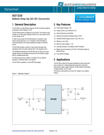
DatasheetAS1320200mA Step-Up DC-DC Converter1 General Description2 Key Features!Fixed Output Voltage: 3.3V!Output Current: Up to 200mA @ 2V!Internal Synchronous Rectifier!Requires No External Schottky Diode or FETsIn order to save power the AS1320 features a shutdown mode,where it draws less than 1µA. In shutdown mode the battery isconnected directly to the output enabling the supply of real-timeclocks.!Shutdown Mode Supply Current: Less Than 1µA!Efficiency: Up to 90%!Minimum Input Voltage: 1.5VThe AS1320 provides a power-on reset output that goes highimpedance when the output reaches 90% of its regulation point.!Accurate Shutdown Low-Battery Cutoff Threshold!Battery Input Connected to Pin OUT in Shutdown Mode forBackup Power!6-pin SOT23 PackageThe AS1320 is a high-efficiency step-up DC-DC converter designedto generate a fixed voltage of 3.3V.The AS1320 achieves an efficiency of up to 90%. The minimum inputvoltage is 1.5V, the output voltage is fixed at 3.3V, and output currentis up to 200mA @ 2V.The SHDNN trip threshold of the AS1320 can be used as an inputvoltage detector that disables the device when the battery voltagefalls to a predetermined level.An internal synchronous rectifier is included, thus an externaltransistor or Schottky diode is not required.The AS1320 is available in a 6-pin SOT23 package.3 ApplicationsThe AS1320 is ideal for low-power applications where ultra-smallsize is critical as in medical diagnostic equipment, hand-heldinstruments, pagers, digital cameras, remote wireless transmitters,cordless phones, and PC cards.The device is also perfect as a local 3.3V supply or as a batterybackup.Figure 1. Application Diagram24 1.5 to COUT22µFR1100kΩRESETN Output3GNDSHDNNwww.austriamicrosystems.com/DC-DC Step-Up/AS1320 3.3VOutput5BATTRevision 1.041 - 12
AS1320Datasheet - P i n A s s i g n m e n t s4 Pin AssignmentsFigure 2. Pin Assignments (Top View)SHDNN1BATT2GND3AS13206RESETN5OUT4LX4.1 Pin DescriptionsTable 1. Pin DescriptionsPin NumberPin NameDescriptionActive-Low Logic Shutdown Input0 The AS1320 is off and the current into BATT is 1µA (typ).1 The AS1320 is on.1SHDNN2BATTBattery Voltage Input3GNDGround4LX5OUT6RESETNExternal Inductor ConnectionOutput VoltageActive-Low reset outputwww.austriamicrosystems.com/DC-DC Step-Up/AS1320Revision 1.042 - 12
AS1320Datasheet - A b s o l u t e M a x i m u m R a t i n g s5 Absolute Maximum RatingsStresses beyond those listed in Table 2 may cause permanent damage to the device. These are stress ratings only, and functional operation ofthe device at these or any other conditions beyond those indicated in Section 6 Electrical Characteristics on page 4 is not implied. Exposure toabsolute maximum rating conditions for extended periods may affect device reliability.Table 2. Absolute Maximum RatingsParameterMinMaxUnitsAll Pins to GND-0.37V1A100mAJEDEC 78500mW(ΘJA 9.1mW/ºC above 70ºC)LX CurrentLatch-Up-100Package Power Dissipation(TAMB 70ºC)Operating Temperature Range-40 85ºCElectrostatic Discharge-500 500VHumidity (Non-Condensing)585%Storage Temperature Range-55125ºCJunction Temperature150ºCPackage Body Temperature260ºCwww.austriamicrosystems.com/DC-DC Step-Up/AS1320Revision 1.04CommentsHBM MIL-Std. 883E 3015.7 methodsThe reflow peak soldering temperature (bodytemperature) specified is in compliance with IPC/JEDECJ-STD-020 “Moisture/ Reflow Sensitivity Classification forNon-Hermetic Solid State Surface Mount Devices”.3 - 12
AS1320Datasheet - E l e c t r i c a l C h a r a c t e r i s t i c s6 Electrical CharacteristicsTAMB -40 to 85ºC, VBATT 2V, VOUT 3.3, VSHDNN 1.5V (unless otherwise specified). Typical values @ TAMB 25ºC.Table 3. Electrical CharacteristicsSymbolParameterVBATTBattery Input RangeConditionsVSUStartup Battery Input VoltageVOUTOutput VoltageRNCHN-ChannelOn-ResistanceRPCHP-Channel On-ResistanceIMAXN-Channel Switch Current LimittONSwitch MaximumOn-TimeSynchronous RectifierZero-Crossing CurrentTAMB 25ºC8TAMB -40 to 85ºC0Typ1.512RLOAD 47Ω, TAMB 25ºC1.22RLOAD 47Ω, TAMB -40 to 85ºC1.24TAMB 25ºC3.267TAMB -40 to 85ºC3.217ILX 100mA, TAMB 25ºC3.3000.3ILX 100mA, TAMB 25ºCShutdown Current into OUTQuiescent Current into BATTShutdown Current into BATT1SHDNN Threshold0.4RESETN Voltage LowRESETN Leakage CurrentLX Leakage CurrentV1.53.3331.21.31.6TAMB 25ºC550TAMB -40 to 85ºC450TAMB 25ºC5TAMB -40 to 85ºC4VOUT 3.5V, TAMB 25ºC700850950791030606535VOUT 3.5V, TAMB -40 to 85ºC5560VSHDNN 0V, TAMB 25ºC0.01VSHDNN 0V, TAMB -40 to 85ºC12VOUT 3.5V, TAMB 25ºC0.01VOUT 3.5V, TAMB -40 to 85ºC12VSHDNN 0V, TAMB 25ºC0.011VSHDNN 0V, TAMB -40 to 85ºC2VBATT 1.5 to 3.5V0.3Rising Edge, TAMB 25ºC1.185Rising Edge, TAMB -40 to 85ºC1.170SHDNN Threshold HysteresisRESETN ThresholdUnit3.51.5ILX 100mA, TAMB -40 to 85ºC1Max3.373ILX 100mA, TAMB -40 to 85ºCQuiescent Current into OUTSHDNN Logic LowMin1.2281.2711.2860.02Falling Edge, TAMB 25ºC2.830Falling Edge, TAMB -40 to 140IRESETN 1mA, VOUT 2.5V,TAMB 25ºC0.15IRESETN 1mA, VOUT 2.5V,TAMB -40 to 85ºC0.2VVVRESETN 5.5V, TAMB 25ºC0.1VRESETN 5.5V, TAMB 85ºC1TAMB 25ºC0.1TAMB 85ºC101001000nAnAILOADMaximum Load CurrentVBATT 2V200mAηEfficiencyVBATT 3V, ILOAD 100mA90%1. Guaranteed by design.2. Voltage which triggers next loading cycle. Ripple and rms value depend on external components.Note: All limits are guaranteed. The parameters with min and max values are guaranteed with production tests or SQC (Statistical QualityControl) methods.www.austriamicrosystems.com/DC-DC Step-Up/AS1320Revision 1.044 - 12
AS1320Datasheet - Ty p i c a l O p e r a t i n g C h a r a c t e r i s t i c s7 Typical Operating CharacteristicsVOUT 3.3V, VBATT 2V, TAMB 25ºC.Figure 3. VOUT vs. VBATT; On, 16ΩFigure 4. VOUT vs. VBATT; On, 330Ω4Output Voltage (V)aOutput Voltage (V)a432132100012304Figure 5. VOUT vs. VBATT; Shutdown, 200mA Load34Figure 6. VOUT vs. VBATT; Shutdown, No Load6655Output Voltage (V)aOutput Voltage (V)a2Battery Voltage (V)Battery Voltage (V)43214321011.522.533.544.5505.50Battery Voltage (V)5002.5Startup Voltage (V)a34003002001.510.5002.56210024Figure 8. Startup Voltage vs. Load Resistance6001.52Battery Voltage (V)Figure 7. Maximum Output Current vs. VBATTMaximum Output Current (mA)a133.510100010000Load Resistance (Ω)Battery Voltage (V)www.austriamicrosystems.com/DC-DC Step-Up/AS1320100Revision 1.045 - 12
AS1320Datasheet - Ty p i c a l O p e r a t i n g C h a r a c t e r i s t i c sIOUTVIN100mV/Div200mA1V/DivVOUT(AC Coupled)VOUT(AC Coupled)Figure 10. Load Transient100mV/DivFigure 9. Line Transient2mA100µs/Div100µs/DivFigure 11. On/Off Response; RLOAD e 12. Shutdown Response; RLOAD 33Ω100µs/Div200µs/DivFigure 13. Switching Waveforms; RLOAD 33ΩFigure 14. Efficiency vs. Load CurrentIL500mAVBATT 3V90Efficiency (%)2V/DivVLX100mV/DivVOUT(AC Coupled)95VBATT 2.5V85VBATT 2V80VBATT 1.5V757065110µs/Div101001000Load Current (mA)www.austriamicrosystems.com/DC-DC Step-Up/AS1320Revision 1.046 - 12
AS1320Datasheet - D e t a i l e d D e s c r i p t i o n8 Detailed DescriptionThe AS1320 is a high-efficiency, compact step-up converter with 35µA quiescent supply current which ensures the highest efficiency over a wideload range. With a minimum of 1.5V input voltage, the device is well suited for applications with one- or two-cells, such as lithium ion (Li ),nickel-metal-hydride (NiMH), or alkaline.Figure 15. Block Diagram 1.5 to 3.5VBatteryCIN22µFZeroCrossingDetector410µH LXBATTOUT � 1.228VVREFCurrentLimiter–1AS1320SHDNN 3.3VOutput 1.1V 6RESETNGND 3The input battery is connected to the device through an inductor and an internal P-FET when pin SHDNN is low. In this state, the step-upconverter is off and the voltage drop across the P-FET body diode is eliminated, and the input battery can be used as a battery-backup or realtime-clock supply.The built-in synchronous rectifier significantly improves efficiency and reduces PCB circuit size and costs by eliminating the need for an externalSchottky diode.8.1 Control CircuitryThe AS1320 integrated current-limited key circuitry provides low quiescent current and extremely-high efficiency over a wide VOUT rangewithout the need for an oscillator. Inductor current is limited by the 7µs switch maximum on-time or by the 0.7A N-channel current limit. At eachcycle, the inductor current must ramp down to zero after the on-time before the next cycle may start. When the error comparator senses that theoutput has fallen below the regulation threshold, another cycle begins.An internal synchronous rectifier eliminates the need for an external Schottky diode, thereby reducing costs and PCB surface area. As theinductor discharges, the P-channel MOSFET turns on and shunts the MOSFET body diode, resulting in a significant reduction of the rectifiervoltage drop, improving efficiency without external components.www.austriamicrosystems.com/DC-DC Step-Up/AS1320Revision 1.047 - 12
AS1320Datasheet - D e t a i l e d D e s c r i p t i o n8.2 ShutdownWhen pin SHDNN is low the AS1320 is switched off and no current is drawn from battery; when pin SHDNN is high the device is switched on. IfSHDNN is driven from a logic-level output, the logic high-level (on) should be referenced to VOUT to avoid intermittently switching the device on.Note: If pin SHDNN is not used, it should be connected directly to pin OUT.In shutdown the battery input is connected to the output through the inductor and the internal synchronous rectifier P-FET. This allows the inputbattery to provide backup power for devices such as an idle microcontroller, memory, or real-time-clock, without the usual diode forward drop. Inthis way a separate backup battery is not needed.In cases where there is residual voltage during shutdown, some small amount of energy will be transferred from pin OUT to pin BATTimmediately after shutdown, resulting in a momentary spike of the voltage at pin BATT. The ratio of CIN and COUT partly determine the size andduration of this spike, as does the current-sink ability of the input device.8.3 Low-Battery CutoffThe AS1320 SHDNN trip threshold (1.228V) can be used as an input voltage detector that disables the device when the battery input voltagefalls to a pre-set level. An external resistor-divider network can be used to set the battery-detection voltage (see Figure 16).Figure 16. Low-Battery Cutoff Application Diagram2 1.5 to 01R21MΩ10nFR3100kΩ6RESETNCOUT22µF 3.3VOutputPower-OnReset3GNDSHDNNFor the resistor-divider network shown in Figure 16, calculate the value for R1 by:R1 R2 x ((VOFF/VSHDNN) - 1)(EQ 1)Where:VOFF is the battery voltage at which the AS1320 shuts down.VSHDNN 1.228VThe value of R2 should be between 100kΩ and 1MΩ to minimize battery drain.Note: Input ripple can cause false shutdowns, therefore to minimize the effect of ripple, a low-value capacitor from SHDNN to GND should beused to filter out input noise. The value of the capacitor should be such that the R/C time constant is 2ms.8.4 Power-On ResetThe AS1320 provides a power-on reset output (RESETN) that goes high-impedance when the output reaches 90% of its regulation point.RESETN goes low when the output is below 90% of the regulation point. A 100kΩ to 1MΩ pullup resistor between pin RESETN and pin OUTcan provide a microprocessor logic control signal.Note: Connect pin RESETN to GND when the power-on reset feature is not used.www.austriamicrosystems.com/DC-DC Step-Up/AS1320Revision 1.048 - 12
AS1320Datasheet - A p p l i c a t i o n I n f o r m a t i o n9 Application Information9.1 Inductor SelectionThe control circuitry of the AS1320 permits a wide range of inductor values to be selected – from 4.7 to 47µH; 10µH is ideal for mostapplications.The intended application should dictate the value of L. The trade-off between required PCB surface area and desired output ripple are thedetermining factors: smaller values for L require less PCB space, larger values of L reduce output ripple. If the value of L is large enough toprevent IMAX from being reached before tON expires, the AS1320 output power will be reduced.For maximum output current calculate the value for L as:(VBATT(MAX) (1µs))/0.7A L (VBATT(MIN)(7µs))/0.7A(EQ 2)IOUT(MAX) [(0.7A/2)(VBATT(MIN) - (0.7A/2)(RNCH RIND))]/VOUT(EQ 3)Where:RIND is the inductor series resistance.RNCH is the RDS(ON) of the N-channel MOSFET (0.3Ω typ).Note: Coils should be able to handle 500mARMS and have a ISAT 1A and should have a RIND 100mΩ.9.2 Capacitor Selection9.2.1COUT SelectionChoose a COUT value to achieve the desired output ripple percentage. A 22µF ceramic capacitor is a good initial value. The value for COUT canbe determined by:2COUT (L 2.5µH) x VBATT(MAX) / r%(EQ 4)Where:r is the desired output ripple in %.9.2.2CIN SelectionCIN reduces the peak current drawn from the battery and can be the same value as COUT. A larger value for CIN can be used to further reduceripple and improve AS1320 efficiency.9.3 PC Board Layout and GroundingWell-designed printed circuit-board layout is important for minimizing ground bounce and noise.!Place pin GND lead and the ground leads of CIN and COUT as close to the device as possible.!Keep the lead to pin LX as short as possible.!To maximize output power and efficiency and minimize output ripple voltage, use a ground plane and solder the GND pin directly to theground plane.www.austriamicrosystems.com/DC-DC Step-Up/AS1320Revision 1.049 - 12
AS1320Datasheet - P a c k a g e D r a w i n g s a n d M a r k i n g s10 Package Drawings and MarkingsThe AS1320 is available in a 6-pin SOT23 package.Figure 17. 6-pin SOT23 PackageNotes:1. All dimensions are in millimeters.2. Foot length is measured at the intercept point between datum A and leadsurface.3. Package outline exclusive of mold flash and metal burr.4. Pin 1 is the lower left pin when reading the top mark from left to right.5. Pin 1 identifier dot is 0.3mm.φ min and is located above pin 1.6. Meets JEDEC MO178.www.austriamicrosystems.com/DC-DC Step-Up/AS1320Revision .550.95 REF0º10º10 - 12
AS1320Datasheet - O r d e r i n g I n f o r m a t i o n11 Ordering InformationThe AS1320 is available as the standard products shown in Table 4.Table 4. Ordering InformationOrdering CodeMarkingDescriptionDelivery FormPackageAS1320-TASD7200mA Step-Up DC-DC ConverterTape and Reel6-pin SOT23Note: All products are RoHS compliant.Buy our products or get free samples online at ICdirect: al Support is found at rtFor further information and requests, please contact us mailto:sales@austriamicrosystems.comor find your local distributor at gn the AS1320 online at ogbench is a powerful design and simulation support tool that operates in on-line and off-line mode to evaluate performance andgenerate application-specific bill-of-materials for austriamicrosystems' power management devices.www.austriamicrosystems.com/DC-DC Step-Up/AS1320Revision 1.0411 - 12
AS1320DatasheetCopyrightsCopyright 1997-2010, austriamicrosystems AG, Tobelbaderstrasse 30, 8141 Unterpremstaetten, Austria-Europe. Trademarks Registered .All rights reserved. The material herein may not be reproduced, adapted, merged, translated, stored, or used without the prior written consent ofthe copyright owner.All products and companies mentioned are trademarks or registered trademarks of their respective companies.DisclaimerDevices sold by austriamicrosystems AG are covered by the warranty and patent indemnification provisions appearing in its Term of Sale.austriamicrosystems AG makes no warranty, express, statutory, implied, or by description regarding the information set forth herein or regardingthe freedom of the described devices from patent infringement. austriamicrosystems AG reserves the right to change specifications and prices atany time and without notice. Therefore, prior to designing this product into a system, it is necessary to check with austriamicrosystems AG forcurrent information. This product is intended for use in normal commercial applications. Applications requiring extended temperature range,unusual environmental requirements, or high reliability applications, such as military, medical life-support or life-sustaining equipment arespecifically not recommended without additional processing by austriamicrosystems AG for each application. For shipments of less than 100parts the manufacturing flow might show deviations from the standard production flow, such as test flow or test location.The information furnished here by austriamicrosystems AG is believed to be correct and accurate. However, austriamicrosystems AG shall notbe liable to recipient or any third party for any damages, including but not limited to personal injury, property damage, loss of profits, loss of use,interruption of business or indirect, special, incidental or consequential damages, of any kind, in connection with or arising out of the furnishing,performance or use of the technical data herein. No obligation or liability to recipient or any third party shall arise or flow out ofaustriamicrosystems AG rendering of technical or other services.Contact InformationHeadquartersaustriamicrosystems AGTobelbaderstrasse 30A-8141 Unterpremstaetten, AustriaTel: 43 (0) 3136 500 0Fax: 43 (0) 3136 525 01For Sales Offices, Distributors and Representatives, please w.austriamicrosystems.com/DC-DC Step-Up/AS1320Revision 1.0412 - 12
Backup Power 6-pin SOT23 Package 3 Applications The AS1320 is ideal for low-power applications where ultra-small size is critical as in medical diagnostic equipment, hand-held instruments, pagers, digital cameras, remote wireless transmitters, cordless phones, and PC cards. The device is also perfect as a local 3.3V supply or as a battery backup.