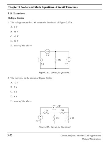
Transcription
UNIT I – BASIC CIRCUIT CONCEPTS– Circuit elements– Kirchhoff’s Law– V-I Relationship of R,L and C– Independent and Dependent sources– Simple Resistive circuits– Networks reduction– Voltage division– current source transformation.- Analysis of circuit using mesh current and nodal voltage methods.1Methods of Analysis
Resistance2Methods of Analysis
Ohm’s Law3Methods of Analysis
Resistors & Passive Sign Convention4Methods of Analysis
Example: Ohm’s Law5Methods of Analysis
Short Circuit as Zero Resistance6Methods of Analysis
Short Circuit as Voltage Source (0V)7Methods of Analysis
Open Circuit8Methods of Analysis
Open Circuit as Current Source (0 A)9Methods of Analysis
Conductance10Methods of Analysis
Circuit Building Blocks11Methods of Analysis
Branches12Methods of Analysis
Nodes13Methods of Analysis
Loops14Methods of Analysis
Overview of Kirchhoff’s Laws15Methods of Analysis
Kirchhoff’s Current Law16Methods of Analysis
Kirchhoff’s Current Law forBoundaries17Methods of Analysis
KCL - Example18Methods of Analysis
Ideal Current Sources: Series19Methods of Analysis
Kirchhoff’s Voltage Law - KVL20Methods of Analysis
KVL - Example21Methods of Analysis
Example – Applying the Basic Laws22Methods of Analysis
Example – Applying the Basic Laws23Methods of Analysis
Example – Applying the Basic Laws24Methods of Analysis
Resistors in Series25Methods of Analysis
Resistors in Parallel26Methods of Analysis
Resistors in Parallel27Methods of Analysis
Voltage Divider28Methods of Analysis
Current Divider29Methods of Analysis
Resistor Network30Methods of Analysis
Resistor Network - Comments31Methods of Analysis
Delta Wye Transformations32Methods of Analysis
Delta Wye Transformations33Methods of Analysis
Example –Delta Wye Transformations34Methods of Analysis
35Methods of Analysis
Methods of Analysis 36IntroductionNodal analysisNodal analysis with voltage sourceMesh analysisMesh analysis with current sourceNodal and mesh analyses by inspectionNodal versus mesh analysisMethods of Analysis
3.2 Nodal Analysis Steps1.2.3.37to Determine Node Voltages:Select a node as the reference node. Assign voltagev1, v2, vn-1 to the remaining n-1 nodes. Thevoltages are referenced with respect to the referencenode.Apply KCL to each of the n-1 nonreference nodes.Use Ohm’s law to express the branch currents interms of node voltages.Solve the resulting simultaneous equations to obtainthe unknown node voltages.Methods of Analysis
Figure 3.1Common symbols for indicating a reference node,(a) common ground, (b) ground, (c) chassis.38Methods of Analysis
Figure 3.239Typical circuit for nodal analysisMethods of Analysis
I 1 I 2 i1 i 2I 2 i 2 i3vhigher vloweri Rv1 0i1 or i1 G1v1R1v1 v2i2 or i2 G2 (v1 v2 )R2v2 0i3 or i3 G3v2R340Methods of Analysis
v1 v1 v2 I1 I2 R1R2v1 v2 v2I2 R2R3 I1 I 2 G1v1 G2 (v1 v2 )I 2 G2 (v1 v2 ) G3v2G1 G2 G241 G2 v1 I1 I 2 G2 G3 v2 I 2 Methods of Analysis
Example 3.1 42Calculus the node voltage in the circuitshown in Fig. 3.3(a)Methods of Analysis
Example 3.1 At node 1i1 i2 i3v1 v2 v1 0 5 4243Methods of Analysis
Example 3.1 At node 2i2 i4 i1 i5v2 v1 v2 0 5 4644Methods of Analysis
Example 3.1 In matrix form: 1 1 2 4 1 4451 v 5 14 1 1 v2 5 6 4 Methods of Analysis
Practice Problem 3.1Fig 3.446Methods of Analysis
Example 3.2 47Determine the voltage at the nodes in Fig.3.5(a)Methods of Analysis
Example 3.2 At node 1,3 i1 ixv1 v3 v1 v2 3 4248Methods of Analysis
Example 3.2 At nodeix i2 2i3v1 v2 v2 v3 v2 0 28449Methods of Analysis
Example 3.2 At node 3i1 i2 2ixv1 v3 v2 v3 2(v1 v2 ) 48250Methods of Analysis
Example 3.2 51In matrix form: 3 4 1 2 3 41 2789 81 4 v1 3 1 v2 0 8 3 v3 0 8 Methods of Analysis
3.3 Nodal Analysis with VoltageSources 52Case 1: The voltage source is connectedbetween a nonreference node and thereference node: The nonreference nodevoltage is equal to the magnitude of voltagesource and the number of unknownnonreference nodes is reduced by one.Case 2: The voltage source is connectedbetween two nonreferenced nodes: ageneralized node (supernode) is formed.Methods of Analysis
3.3 Nodal Analysis with VoltageSourcesi1 i4 i2 i3 v1 v2 v1 v3 v2 0 v3 0 2486 v2 v3 553Fig. 3.7 A circuit with a supernode.Methods of Analysis
54A supernode is formed by enclosing a(dependent or independent) voltage sourceconnected between two nonreference nodesand any elements connected in parallel withit.The required two equations for regulating thetwo nonreference node voltages are obtainedby the KCL of the supernode and therelationship of node voltages due to theMethods of Analysisvoltage source.
Example 3.3 For the circuit shown in Fig. 3.9, find the nodevoltages.2 7 i1 i 2 0v v2 7 1 2 02 4v1 v2 2i155i2Methods of Analysis
Example 3.4Find the node voltages in the circuit of Fig. 3.12.56Methods of Analysis
Example 3.4At suopernode 1-2,v3 v2v1 v4 v1 10 632v1 v2 20 57Methods of Analysis
Example 3.4 At supernode 3-4,v1 v4 v3 v2 v4 v3 361 4v3 v4 3(v1 v4 )58Methods of Analysis
3.4 Mesh Analysis 59Mesh analysis: another procedure foranalyzing circuits, applicable to planar circuit.A Mesh is a loop which does not contain anyother loops within itMethods of Analysis
Fig. 3.1560(a) A Planar circuit with crossing branches,(b) The same circuit redrawn with no crossing branches.Methods of Analysis
Fig. 3.16A nonplanar circuit.61Methods of Analysis
Steps to Determine Mesh Currents:1.2.3.62Assign mesh currents i1, i2, ., in to the n meshes.Apply KVL to each of the n meshes. Use Ohm’slaw to express the voltages in terms of themesh currents.Solve the resulting n simultaneous equations toget the mesh currents.Methods of Analysis
Fig. 3.17A circuit with two meshes.63Methods of Analysis
V1 R1i1 R3 (i1 i2 ) 0 Apply KVL to each mesh. For mesh 1, R22,i2 V2 R3 (i2 i1 ) 0For mesh( R1 R3 )i1 R3i2 V1 R3i1 ( R2 R3 )i2 V264Methods of Analysis
Solve for the mesh currents. R1 R3 R3 R3 i1 V1 R2 R3 i2 V2 Use i for a mesh current and I for a branchcurrent. It’s evident from Fig. 3.17 thatI1 i1 , I 2 i2 ,65I 3 i1 i2Methods of Analysis
Example 3.5 66Find the branch current I1, I2, and I3 usingmesh analysis.Methods of Analysis
Example 3.5 15 5i1 10(i1 i2 ) 10 0For mesh 1,3i1 2i2 16i2 4i2 10(i2 i1 ) 10 0For mesh 2,i1 2i2 1I1 i1 , I 2 i2 , 67I 3 i1 i2We can find i1 and i2 by substitution methodor Cramer’s rule. Then,Methods of Analysis
Example 3.6 68Use mesh analysis to find the current I0 in thecircuit of Fig. 3.20.Methods of Analysis
Example 3.6 Apply KVL to each mesh. For mesh 1, 24 10(i1 i2 ) 12(i1 i3 ) 011i1 5i2 6i3 12 For mesh 2,24i2 4(i2 i3 ) 10(i2 i1 ) 0 5i1 19i2 2i3 069Methods of Analysis
Example 3.6 For mesh 3,4I0 12 ( i 3 i 1 ) 4 ( i 3 i 2 ) 0At nodeA, I0 I 1 i2 ,4 ( i 1 i 2 ) 12 ( i 3 i 1 ) 4 ( i 3 i 2 ) 0 i1 i 2 2 i 3 0 In matrix from Eqs. (3.6.1) to (3.6.3) become 11 5 1 70 519 1 6 i1 12 2 i2 0 2 i3 0 we can calculus i1, i2 and i3 by Cramer’s rule,and find I0.Methods of Analysis
3.5 Mesh Analysis with CurrentSourcesFig. 3.22 A circuit with a current source.71Methods of Analysis
Case 1–Current source exist only in one mesh–One mesh variable is reducedCase 2–72i1 2 ACurrent source exists between two meshes, asuper-mesh is obtained.Methods of Analysis
Fig. 3.23 73a supermesh results when two meshes havea (dependent , independent) current sourcein common.Methods of Analysis
Properties of a SupermeshThe current is not completely ignored1.–2.3.74provides the constraint equation necessary tosolve for the mesh current.A supermesh has no current of its own.Several current sources in adjacency forma bigger supermesh.Methods of Analysis
Example 3.7 75For the circuit in Fig. 3.24, find i1 to i4 usingmesh analysis.Methods of Analysis
76If a supermesh consists of two meshes, two6 i1 14 i 2 equations are needed; one is obtained usingKVL and Ohm’s law to the supermesh and the i1 i 2 6other is obtained by relation regulated due tothe current source.Methods of Analysis20
77Similarly, a supermesh formed from threemeshes needs three equations: one is fromthe supermesh and the other two equationsare obtained from the two current sources.Methods of Analysis
2 i1 4 i 3 8 ( i 3 i 4 ) 6 i 2 0i1 i 2 5i2 i3 i48 ( i 3 i 4 ) 2 i 4 10 078Methods of Analysis
3.6 Nodal and Mesh Analysis byInspectionThe analysis equations can beobtained by direct inspection(a) For circuits with only resistors and independentcurrent sources(b) For planar circuits with only resistors andindependent voltage sources79Methods of Analysis
In the Fig. 3.26 (a), the circuit has twononreference nodes and the node equationsI1 I 2 G1v1 G2 (v1 v2 ) (3.7)I 2 G2 (v1 v2 ) G3v2(3.8) MATRIX G1 G2 G280 G2 v1 I1 I 2 G2 G3 v2 I 2 Methods of Analysis
In general, the node voltage equations interms of the conductance isor simplyGv i G 11 G 12 G 1 N GG 22 G 2 N 21 G N 1 G N 2 G NN v1 v 2 v N i1 i 2 i N where G : the conductance matrix,v : the output vector, i : the input vector81Methods of Analysis
The circuit has two nonreference nodes andthe node equations were derived as R1 R3 R382 R3 i1 v1 R2 R3 i2 v2 Methods of Analysis
In general, if the circuit has N meshes, themesh-current equations as the resistancesR 1 N i1 term is R 11 R 12 v1 R v R 22 R 2 N i 2 21or simply 2 Rv i R N1 RN 2 R NN i N v N where R : the resistance matrix,i : the output vector, v : the input vector83Methods of Analysis
Example 3.8 84Write the node voltage matrix equations inFig.3.27.Methods of Analysis
Example 3.8 The circuit has 4 nonreference nodes, soG11G3311 0 .3 , G510111 0 .5 ,884 22G44111 1 . 325581111 1 . 625821The off-diagonal terms are1 0 . 2 , G 13 G 14 0511 0 . 2 , G 23 0 . 125 , G 24 181 0 , G 32 0 . 125 , G 34 0 . 125G 12 G 21G 3185G 41 0 , G 42 1, G 43 0 . 125Methods of Analysis
Example 3.8i1 3 , i 2 1 2 3 , i 3 0 , i 4 2 4 6 The input current vector i in amperes 86The node-voltage equations are0 .30.200 0.21 .325 0.125 10 0.1250 .5 0.1250 1 0.1251 .625 v1 v 2 v3 v 4 Methods of Analysis3 3 0 6
Example 3.9 87Write the mesh current equations in Fig.3.27.Methods of Analysis
Example 3.9 The input voltage vector v in voltsv1 4 , v2 10 4 6 ,v 3 12 6 6 , v 0, v5 6The mesh-current equations are 8849 2 202210 4 49 100 1080 10 30 i1 1 i2 0 i3 3 i4 4 i 5 4 6 6 0 6 Methods of Analysis
3.7 Nodal Versus Mesh Analysis Both nodal and mesh analyses provide asystematic way of analyzing a complexnetwork.The choice of the better method dictated bytwo factors.––89First factor : nature of the particular network. Thekey is to select the method that results in thesmaller number of equations.Second factor : information required.Methods of Analysis
BJT Circuit Models90(a) dc equivalent model.(b) An npn transistor,Methods of Analysis
Example 3.13 91For the BJT circuit in Fig.3.43, 150 andVBE 0.7 V. Find v0.Methods of Analysis
Example 3.13 92Use mesh analysis or nodal analysisMethods of Analysis
Example 3.1393Methods of Analysis
3.10 SummaryNodal analysis: the application of KCL atthe nonreference nodes1.–A supernode: two nonreference nodesMesh analysis: the application of KVL2.3.–4.94A circuit has fewer node equationsA circuit has fewer mesh equationsA supermesh: two meshesMethods of Analysis
UNIT II – SINUSOIDAL STEADY STATE ANALYSIS–-Phasor– Sinusoidal steady state response concepts of impedance and admittance– Analysis of simple circuits– Power and power factors–– Solution of three phase balanced circuits and three phase unbalanced circuits–-Power measurement in three phase circuits.95Methods of Analysis9
Sinusoidal Steady StateResponse
Sinusoidal Steady StateResponse1. Identify the frequency, angular frequency, peak value, RMS value, andphase of a sinusoidal signal.2. Solve steady-state ac circuits using phasors and complex impedances3. Compute power for steady-state ac circuits.4. Find Thévenin and Norton equivalent circuits.5. Determine load impedances for maximum power transfer.
The sinusoidal function v(t) VM sin t is plotted (a) versus t and (b) versus t.
The sine wave VM sin ( t ) leads VM sin t by radian
Frequency1f T2 Angular frequency T 2 fosin z cos( z 90 )osin t cos( t 90 )osin( t 90 ) cos t
Representation of the two vectors v1and v2.In this diagram, v1 leads v2 by 100o 30o 130o, although itcould also be argued that v2 leads v1 by 230o.Generally we express the phase difference by an angle lessthan or equal to 180o in magnitude.
Euler’s identity t 2 fA cos t A cos 2 f tIn Euler expression,A cos t Real (A e j t )A sin t Im( A e j t )Any sinusoidal function canbe expressed as in Eulerform.4-6
Applying Euler’s IdentityThe complex forcing function Vm e j ( t ) produces the complexresponse Im e j ( t ).
The sinusoidal forcing function Vm cos ( t θ) produces thesteady-state response Im cos ( t φ).The imaginary sinusoidal input j Vm sin ( t θ) produces theimaginary sinusoidal output response j Im sin ( t φ).
Re(Vm e j ( t ) ) Re(Im e j ( t ))Im(Vm e j ( t ) ) Im(Im e j ( t ))
Phasor DefinitionTime function : v1 t V1 cos ωt θ1 Phasor: V1 V1 1V1 Re(ej ( t 1 )V1 Re(ej ( 1 ))) by dropping t
A phasor diagram showing the sum ofV1 6 j8 V and V2 3 – j4 V,V1 V2 9 j4 V VsVs Ae j θA [9 2 4 2]1/2θ tan -1 (4/9)Vs 9.85 24.0o V.
Phasors AdditionStep 1: Determine the phase for each term.Step 2: Add the phase's using complex arithmetic.Step 3: Convert the Rectangular form to polar form.Step 4: Write the result as a time function.
Conversion of rectangular topolar form v1 t 20 cos( t 45 ) v2 (t ) 10 cos( t 30 ) V1 20 45V2 10 30
Vs V1 V2 20 45 10 30 14.14 j14.14 8.660 j 5 23.06 j19.14 29.97 39.7Vs Ae j 19.14A 23.06 ( 19.14) 29.96, tan 39.7 23.0622 1v s t 29.97 cos t 39.7
Phase relation ship
COMPLEX IMPEDANCEVL j L I LZ L j L L 90VL Z L I L
(a)(b)In the phasor domain,(a) a resistor R is represented by animpedance of the same value;(b) a capacitor C is represented by animpedance 1/j C;(c) an inductor L is represented by animpedance j L.(c)
V Vej tdVd Ve j tI C C j CVedtdtV1I j C V ZcIj Cj tZc is defined as the impedance of a capacitorThe impedance of a capacitor is 1/j C.As I j C V, if v V cos t , then i CV cos ( t 90 )
As I j C V, if v VM cos t , then i CVM cos ( t 90 )I M CVM
I Ie j tdId Ie j tV L L j LIedtdtVV j L I j L Z LIZL is the impedance of an inductor.The impedance of a inductor is j LAs V j C I, if i I cos t , then v LI cos ( t 90 )or i I cos ( t 90 ), and v LI cos t.j t
As V j CI, if i IM cos t, thenv LIM cos( t 90 )ori IM cos( t 90 ), and v LIM cos t, VM LIM
Complex Impedance in PhasorNotationVC ZC I C111 ZC j 90j C C CVL Z L I LZ L j L L 90 VR RI R
Kirchhoff’s Laws in Phasor FormWe can apply KVL directly to phasors. Thesum of the phasor voltages equals zero forany closed path.The sum of the phasor currents entering anode must equal the sum of the phasorcurrents leaving.
Ztotal 100 j(150 50) 100 j100 141.4 45 V100 30 I 0.707 30 45Ztotal 141.4 45 0.707 15 VR 100 I 70.7 15 , vR (t ) 70.7 cos(500t 15 )VL j150 I 150 90 0.707 15 106.05 90 15 106.05 75 , vL (t ) 106.05cos(500t 75 )VC j50 I 50 90 0.707 15 35.35 90 15 35.35 105 , vL (t ) 35.35cos(500t 105 )
11Z RC 1 / R 1 / Zc 1 / 100 1 /( j100)11j j 0.01As j0.012 j100 j100 j jZ RC11 0 70.71 450.01 j 0.01 0.01414 45 50 j50
Z RCVc Vs( voltage division)Z L Z RC 70.71 4570.71 45 10 90 10 90 j100 50 j5050 j50 70.71 45 10 45 10 13570.71 45 vc (t ) 10 cos (1000t 135 ) 10 cos 1000t V
I VsZ L Z RC10 90 10 90 j100 50 j5050 j5010 90 0.414 13570.71 45 i (t ) 0.414 cos (1000t 135 )
VCIR R10 135 0.1 135 100iR (t ) 0.1 cos (1000t 135 )VC 10 135 10 135 IC 0.1 45Zc j100100 90 iR (t ) 0.1 cos (1000t 45 ) A
Solve by nodal analysisV1 V1 V2 2 90 j 2 eq(1)10 j5V2 V2 V1 1.5 0 1.5eq(2)j10 j5
V1 V1 V2V2 V2 V1 2 90 j 2 eq(1) 1.5 0 1.510 j5j10 j5From eq (1)1 1 jj10.1V1 j0.2V1 j0.2V2 j 2 As j, jj j j 1 j(0.1 j0.2)V1 j0.2V2 j 2From eq (2) j0.2V1 j0.1V2 1.5SolvingV1 by eq(1) 2 eq(2)(0.1 j0.2)V1 3 j 23 j23.6 33.69 V1 16.1 33.69 63.430.1 j0.2 0.2236 63.43 16.1 29.74 v1 16.1cos(100t 29.74 ) Veq(2)
Vs - j10, ZL j L j(0.5 500) j250Use mesh analysis,
Vs V R V Z 0 ( j10 ) I 250 I ( j 250 ) 0 j1010 90 I 0 . 028 90 45 250 j 250353 .33 45I 0 . 028 135 i 0 . 028 cos( 500 t 135 ) AV L I Z L ( 0 . 028 135 ) 250 90 7 45 v L ( t ) 7 cos( 500 t 45 ) VV R I R ( 0 . 028 135 ) 250 7 135 v R ( t ) 7 cos( 500 t 135 )
AC Power CalculationsP Vrms I rms cos PF cos v iQ Vrms I rms sin
apparent power Vrms I rms2P Q Vrms I rms 2P IQ I2rms2rmsRX2P Q V2RrmsRV2XrmsX
THÉVENIN EQUIVALENTCIRCUITS
The Thévenin voltage is equal to the open-circuitphasor voltage of the original circuit.Vt VocWe can find the Thévenin impedance byzeroing the independent sources anddetermining the impedance looking into thecircuit terminals.
The Thévenin impedance equals the open-circuitvoltage divided by the short-circuit current.Voc VtZ t I scI scI n I sc
Maximum Power Transfer If the load can take on any complex value,maximum power transfer is attained for a loadimpedance equal to the complex conjugate ofthe Thévenin impedance. If the load is required to be a pureresistance, maximum power transfer isattained for a load resistance equal to themagnitude of the Thévenin impedance.
UNIT III–NETWORK THEOREMS (BOTH AC AND DC CIRCUITS)– Superposition theorem– The venin’s theorem- Norton’s theorem-Reciprocity theorem- Maximum power transfer theorem.1619
9.1 – Introduction This chapter introduces importantfundamental theorems of network analysis.They are the Superposition theorem Thévenin’s theorem Norton’s theorem Maximum power transfer theorem Substitution Theorem Millman’s theorem Reciprocity theorem
9.2 – Superposition Theorem Used to find the solution to networks with two ormore sources that are not in series or parallel. The current through, or voltage across, anelement in a network is equal to the algebraic sumof the currents or voltages producedindependently by each source. Since the effect of each source will bedetermined independently, the number ofnetworks to be analyzed will equal the number ofsources.
Superposition Theorem The total power delivered to a resistive elementmust be determined using the total current throughor the total voltage across the element and cannotbe determined by a simple sum of the powerlevels established by each source.
9.3 – Thévenin’s Theorem Any two-terminal dc network can bereplaced by an equivalent circuit consistingof a voltage source and a series resistor.
Thévenin’s Theorem Thévenin’s theorem can be used to: Analyze networks with sources that are not in series orparallel. Reduce the number of components required toestablish the same characteristics at the outputterminals. Investigate the effect of changing a particularcomponent on the behavior of a network without havingto analyze the entire network after each change.
Thévenin’s Theorem Procedure to determine the proper values of RTh andETh Preliminary1. Remove that portion of the network across which theThévenin equation circuit is to be found. In the figurebelow, this requires that the load resistor RL betemporarily removed from the network.
Thévenin’s Theorem2. Mark the terminals of the remaining two-terminal network. (Theimportance of this step will become obvious as we progressthrough some complex networks.)RTh:3. Calculate RTh by first setting all sources to zero (voltagesources are replaced by short circuits, and current sources byopen circuits) and then finding the resultant resistancebetween the two marked terminals. (If the internal resistanceof the voltage and/or current sources is included in the originalnetwork, it must remain when the sources are set to zero.)
Thévenin’s TheoremETh:4. Calculate ETh by first returning all sources to their originalposition and finding the open-circuit voltage between themarked terminals. (This step is invariably the one that will leadto the most confusion and errors. In all cases, keep in mindthat it is the open-circuit potential between the two terminalsmarked in step 2.)
Thévenin’s Theorem Conclusion:5.Draw the Thévenin equivalentcircuit with the portion of thecircuit previously removedreplacedbetweentheterminals of the equivalentcircuit. This step is indicatedby the placement of theresistor RL between theterminals of the Théveninequivalent circuit.Insert Figure 9.26(b)
Experimental Procedures Two popular experimental procedures for determiningthe parameters of the Thévenin equivalentnetwork: Direct Measurement of ETh and RTh For any physical network, the value of ETh can be determinedexperimentally by measuring the open-circuit voltage acrossthe load terminals. The value of RTh can then be determined by completing thenetwork with a variable resistance RL.
Thévenin’s Theorem Measuring VOC and ISC The Thévenin voltage is again determined bymeasuring the open-circuit voltage across the terminalsof interest; that is, ETh VOC. To determine RTh, a shortcircuit condition is established across the terminals ofinterest and the current through the short circuit (Isc) ismeasured with an ammeter. Using Ohm’s law:RTh Voc / Isc
Vth173
Rth174
Norton’s Theorem Norton’s theorem states the following: Any two-terminal linear bilateral dc network can bereplaced by an equivalent circuit consisting of acurrent and a parallel resistor. The steps leading to the proper values of IN andRN. Preliminary steps:1. Remove that portion of the network across which theNorton equivalent circuit is found.2. Mark the terminals of the remaining two-terminalnetwork.
Norton’s Theorem Finding RN:3. Calculate RN by first setting all sources to zero (voltagesources are replaced with short circuits, and currentsources with open circuits) and then finding theresultant resistance between the two marked terminals.(If the internal resistance of the voltage and/or currentsources is included in the original network, it mustremain when the sources are set to zero.) Since RN RTh the procedure and value obtained using theapproach described for Thévenin’s theorem willdetermine the proper value of RN.
Norton’s Theorem Finding IN :4. Calculate IN by first returning all the sources to theiroriginal position and then finding the short-circuitcurrent between the marked terminals. It is the samecurrent that would be measured by an ammeterplaced between the marked terminals. Conclusion:5. Draw the Norton equivalent circuit with the portion ofthe circuit previously removed replaced between theterminals of the equivalent circuit.
178
9.5 – MMaximum PowerTransfer Theorem The maximum power transfer theoremstates the following:A load will receive maximum power from anetwork when its total resistive value isexactly equal to the Thévenin resistanceof the network applied to the load. Thatis,RL RTh
Maximum Power Transfer Theorem For loads connected directly to a dc voltage supply, maximum power will bedelivered to the load when the load resistance is equal to the internalresistance of the source; that is, when:RL Rint
Reciprocity Theorem The reciprocity theorem is applicable only tosingle-source networks and states the following: The current I in any branch of a network, due to asingle voltage source E anywhere in the network, willequal the current through the branch in which thesource was originally located if the source is placed inthe branch in which the current I was originallymeasured. The location of the voltage source and the resulting currentmay be interchanged without a change in current
UNIT IV - TRANSIENT RESPONSE FOR DC CIRCUITS–– Transient response of RL, RC and RLC–– Laplace transform for DC input with sinusoidal input.
Solution to First Order Differential EquationConsider the general Equationdx(t ) x(t ) K s f (t )dtLet the initial condition be x(t 0) x( 0 ), then we solve the differentialequation:dx(t ) x(t ) K s f (t )dtThe complete solution consists of two parts: the homogeneous solution (natural solution) the particular solution (forced solution)
The Natural ResponseConsider the general Equationdx(t ) x(t ) K s f (t )dtSetting the excitation f (t) equal to zero,dx N (t )dx N (t )x N (t ) dx N (t )dt x N (t ) 0 or , dtdt x N (t ) dx N (t )dt , x N (t ) x N (t ) e t / It is called the natural response.
The Forced ResponseConsider the general Equationdx(t ) x(t ) K s f (t )dtSetting the excitation f (t) equal to F, a constant for t 0dxF (t ) xF (t ) K S FdtxF (t ) K S F for t 0 It is called the forced response.
The Complete ResponseSolve for ,Consider the general Equationdx(t ) x(t ) K s f (t )dtThe complete response is: the natural response the forced responsefor t 0x(t 0) x(0) x( ) x(0) x( )The Complete solution:x x N (t ) x F (t ) e t / K S F e t / x ( )x (t ) [ x(0) x( )] e t / x ( )[ x(0) x( )] e t / called transient responsex ( ) called steady state response
TRANSIENT RESPONSEFigure 5.1
A general model of the transientCircuit with switched DC excitationFigure5.2,5.3analysis problem
For a circuit containing energy storage elementFigure 5.5, 5.6
(a) Circuit at t 0(b) Same circuit a long time after the switch is closedFigure5.9, 5.10The capacitor acts as open circuit for the steady state condition(a long time after the switch is closed).
(a) Circuit for t 0(b) Same circuit a long time before the switch is openedThe inductor acts as short circuit for the steady state condition(a long time after the switch is closed).
Reason for transient response The voltage across a capacitor cannot bechanged instantaneously. VC (0 ) VC (0 ) The current across an inductor cannot bechanged instantaneously. I L (0 ) I L (0 )
ExampleFigure5.12, 5.135-6
Transients Analysis1. Solve first-order RC or RL circuits.2. Understand the concepts of transientresponse and steady-state response.3. Relate the transient response of firstordercircuits to the time constant.
TransientsThe solution of the differential equationrepresents are response of the circuit. Itis called natural response.The response must eventually die out,and therefore referred to as transientresponse.(source free response)
Discharge of a Capacitance through aResistance i 0,iciRiC iR 0dvC t vC t C 0dtRSolving the above equationwith the initial conditionVc(0) Vi
Discharge of a Capacitance through aResistancedvC t vC t C 0dtRdvC t RC vC t 0dtvC t KestststRCKse Ke 0 1s RC t RCvC t Ke vC (0 ) Vi Ke KvC t Vi e0 / RC t RC
vC t Vi e tRCExponential decay waveformRC is called the time constant.At time constant, the voltage is36.8%of the initial voltage.vC t Vi (1 e t RC )Exponential rising waveformRC is called the time constant.At time constant, the voltage is 63.2%of the initial voltage.
RC CIRCUITfor t 0-, i(t) 0u(t) is voltage-step function Vu(t)
RC CIRCUITVu(t)iR iCvu (t ) vCdvCiR , iC CRdtdvCRC vC V , v u (t ) V for t 0dtSolving the differential equation
Complete ResponseComplete response natural response forced response Natural response (source free response)is due to the initial condition Forced response is the due to theexternal excitation.
Figure5.17,5.18a). Complete, transient and steady stateresponseb). Complete, natural, and forced responsesof the circuit5-8
Circuit Analysis for RC CircuitApply KCLiR iCvs v RdvCiR , iC CRdtdvC11 vR vsdtRCRCvs is the source applied.
Solution to First Order Differential EquationConsider the general Equationdx(t ) x(t ) K s f (t )dtLet the initial condition be x(t 0) x( 0 ), then we solve the differentialequation:dx(t ) x(t ) K s f (t )dtThe comple
UNIT I - BASIC CIRCUIT CONCEPTS - Circuit elements - Kirchhoff's Law - V-I Relationship of R,L and C - Independent and Dependent sources - Simple Resistive circuits - Networks reduction - Voltage division - current source transformation. - Analysis of circuit using mesh current and nodal voltage methods. 1 Methods of Analysis