Transcription
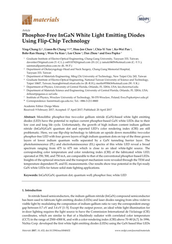
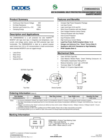
ZXMS6006DGQGreen60V N-CHANNEL SELF PROTECTED ENHANCEMENT MODEIntelliFET MOSFETProduct SummaryFeatures and Benefits Continuous Drain Source VoltageOn-State ResistanceNominal Load Current (VIN 5V)60V100m 2.8A Clamping Energy490mJDescription and ApplicationsTMThe ZXMS6006DGQ is a self protected low side IntelliFETMOSFET with logic level input. It integrates over-temperature, overcurrent, over-voltage (active clamp) and ESD protected logic levelfunctionality. The ZXMS6006DGQ is ideal as a general purposeswitch driven from 3.3V or 5V microcontrollers in harsh environmentswhere standard MOSFETs are not rugged enough. Lamp DriverMotor DriverRelay DriverSolenoid Driver Compact High Power Dissipation PackageLow Input CurrentLogic Level Input (3.3V and 5V)Short Circuit Protection with Auto RestartOver Voltage Protection (Active Clamp)Thermal Shutdown with Auto RestartOver-Current ProtectionInput Protection (ESD)High Continuous Current RatingLead-Free Finish; RoHS Compliant (Notes 1 & 2)Halogen and Antimony Free. “Green” Device (Note 3)Qualified to AEC-Q101 Standards for High ReliabilityPPAP Capable (Note 4)Mechanical Data Case: SOT223 (Type DN)Case Material: Molded Plastic, “Green” Molding Compound. ULFlammability Classification Rating 94V-0Moisture Sensitivity: Level 1 per J-STD-020Terminals: Matte Tin Finish e3Weight: 0.112 grams (Approximate)SOT223 (Type DN)DSDDININSTop ViewTop ViewPin OutDevice SymbolOrdering Information (Note 5)Part NumberZXMS6006DGQTANotes:MarkingZXMS6006DReel Size (inches)7Tape Width (mm)12Quantity Per Reel1,000 Units1. EU Directive 2002/95/EC (RoHS), 2011/65/EU (RoHS 2) & 2015/863/EU (RoHS 3) compliant. All applicable RoHS exemptions applied.2. See https://www.diodes.com/quality/lead-free/ for more information about Diodes Incorporated’s definitions of Halogen- and Antimony-free, "Green" andLead-free.3. Halogen- and Antimony-free "Green” products are defined as those which contain 900ppm bromine, 900ppm chlorine ( 1500ppm total Br Cl) and 1000ppm antimony compounds.4. Automotive products are AEC-Q101 qualified and are PPAP capable. Please refer to https://www.diodes.com/quality/.5. For packaging details, go to our website at odes-packaging/.Marking InformationZXMS6006D Product Type Marking CodeYWW Date Code MarkingY or Y Last Digit of Year (ex: 8 2018)WW or WW Week Code (01 to 53)IntelliFET is a trademark of Diodes Incorporated.ZXMS6006DGQDocument number: DS37134 Rev. 6 - 21 of 8www.diodes.comJuly 2018 Diodes Incorporated
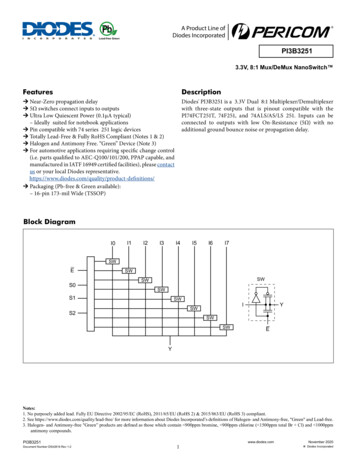
ZXMS6006DGQFunctional Block DiagramdV/dtLimitationMaximum Ratings (@TA 25 C, unless otherwise specified.)CharacteristicContinuous Drain-Source VoltageDrain-Source Voltage for Short Circuit ProtectionContinuous Input VoltageSymbolValueUnitVDS60VVDS(SC)16VVIN-0.5 to 6.0VContinuous Input Current @-0.2V VIN 6VContinuous Input Current @VIN -0.2V or VIN 6VIINNo limit IIN 2mAPulsed Drain Current @VIN 3.3VIDM11APulsed Drain Current @VIN 5VIDM13AContinuous Source Current (Body Diode) (Note 6)IS2APulsed Source Current (Body Diode)ISM12AUnclamped Single Pulse Inductive Energy,TJ 25 C, ID 0.5A, VDD 24VEAS490mJElectrostatic Discharge (Human Body Model)VESD4000VCharged Device ModelVCDM1000VThermal Characteristics (@TA 25 C, unless otherwise specified.)SymbolValueUnitPower Dissipation at TA 25 C (Note 6)Linear Derating FactorCharacteristicPD1.310.4WmW/ CPower Dissipation at TA 25 C (Note 7)Linear Derating FactorPD3.024WmW/ CRθJA96 C/WThermal Resistance, Junction to Ambient (Note 7)RθJA42 C/WThermal Resistance, Junction to Case (Note 8)RθJC12 C/WTJ-40 to 150 CTSTG-55 to 150 CThermal Resistance, Junction to Ambient (Note 6)Operating Temperature RangeStorage Temperature RangeNotes:6. For a device surface mounted on 15mm x 15mm single sided 1oz weight copper on 1.6mm FR-4 board, in still air conditions.7. For a device surface mounted on 50mm x 50mm single sided 2oz weight copper on 1.6mm FR-4 board, in still air conditions.8. Thermal resistance between junction and the mounting surfaces of drain and source pins.ZXMS6006DGQDocument number: DS37134 Rev. 6 - 22 of 8www.diodes.comJuly 2018 Diodes Incorporated
ZXMS6006DGQRecommended Operating ConditionsThe ZXMS6006DGQ is optimized for use with µC operating from 3.3V and 5V supplies.CharacteristicSymbolMinMaxInput Voltage RangeVIN05.5UnitVAmbient Temperature RangeTA-40 125 CHigh Level Input Voltage for MOSFET to be onVIH35.5VLow level input voltage for MOSFET to be offVIL00.7VPeripheral Supply Voltage (voltage to which load is referred)VP016VThermal Characteristics50x50x1.6mmSingle 2oz FR-415x15x1.6mmSingle 1oz FR-415x15x1.6mmSingle 1oz FR-415x15x1.6mmSingle 1oz FR-4TA 25 CZXMS6006DGQDocument number: DS37134 Rev. 6 - 215x15x1.6mmSingle 1oz FR-4Single PulseTA 25 C3 of 8www.diodes.comJuly 2018 Diodes Incorporated
ZXMS6006DGQElectrical Characteristics(@TA 25 C, unless otherwise specified.)CharacteristicStatic CharacteristicsSymbolMinTypMaxUnitDrain-Source Clamp VoltageVDS(AZ)606570V——1Off State Drain CurrentIDSS——2Input Threshold ��48—613—tD(ON)—8.6—Input CurrentIINInput Current While Over Temperature Active—Static Drain-Source On-State ResistanceRDS(ON)Continuous Drain Current (Note 6)IDContinuous Drain Current (Note 7)Current Limit (Note 9)ID(LIM)µAVµAµAm Test ConditionID 10mAVDS 12V, VIN 0VVDS 36V, VIN 0VVDS VGS, ID 1mAVIN 3VVIN 5VVIN 5VVIN 3V, ID 1AVIN 5V, ID 1AVIN 3V, TA 25 CAVIN 5V, TA 25 CVIN 3V, TA 25 CVIN 5V, TA 25 CAVIN 3VVIN 5VDynamic CharacteristicsTurn On Delay TimeRise TimeTurn Off Delay TimeFall TimetR—18—tD(OFF)—34—tF—15—TJT 150 175— C—ff— 10— C—µsVDD 12V, ID 1A, VGS 5VOver-Temperature ProtectionThermal Overload Trip Temperature (Note 10)Thermal Hysteresis (Note 10)Notes:9.The drain current is restricted only when the device is in saturation (see graph ‘Typical Output Characteristic’). This allows the device to be used in the fullyon state without interference from the current limit. The device is fully protected at all drain currents, as the low power dissipation generated outsidesaturation makes current limit unnecessary.10. Over-temperature protection is designed to prevent device destruction under fault conditions. Fault conditions are considered as “outside” normaloperating range, so this part is not designed to withstand over-temperature for extended periods.ZXMS6006DGQDocument number: DS37134 Rev. 6 - 24 of 8www.diodes.comJuly 2018 Diodes Incorporated
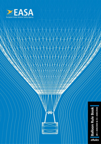
ZXMS6006DGQTypical CharacteristicsVIN VDSID 1mAID 1ATJ 150 CTJ 25 CTJ 150 CVIN 3VTJ 25 CVIN 5VZXMS6006DGQDocument number: DS37134 Rev. 6 - 25 of 8www.diodes.comJuly 2018 Diodes Incorporated
ZXMS6006DGQDrain-Source Voltage (V)Drain-Source Voltage (V)Typical Characteristics (Cont.)12ID 1A10VDS86VIN420-5005010015020025030012VDS10ID 1A864VIN20-50050100150200250300Time ( s)Time ( s)Switching SpeedSwitching SpeedID Drain Current (A)1816VIN 5V14VDS 16VRD 0 121086420051015Time (ms)Typical Short Circuit ProtectionZXMS6006DGQDocument number: DS37134 Rev. 6 - 26 of 8www.diodes.comJuly 2018 Diodes Incorporated
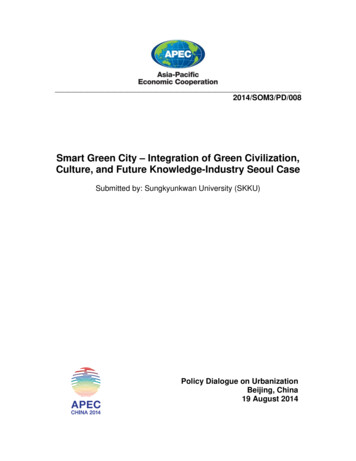
ZXMS6006DGQPackage Outline DimensionsPlease see http://www.diodes.com/package-outlines.html for the latest version.SOT223 (Type DN)Db2CE1EGaugePlane0.25SeatingPlaneeLbe1ASOT223 (Type DN)Dim Min Max TypA-1.70-A10.01 0.15-A21.50 1.68 1.60b0.60 0.80 0.70b22.90 3.10-c0.20 0.32-D6.30 6.70-E6.70 7.30-E13.30 3.70-e--2.30e1--4.60L0.85--All Dimensions in mmA1A2Suggested Pad LayoutPlease see http://www.diodes.com/package-outlines.html for the latest version.SOT223 (Type DN)X1Y1C1Dimensions Value (in 6006DGQDocument number: DS37134 Rev. 6 - 2C7 of 8www.diodes.comJuly 2018 Diodes Incorporated
ZXMS6006DGQIMPORTANT NOTICEDIODES INCORPORATED MAKES NO WARRANTY OF ANY KIND, EXPRESS OR IMPLIED, WITH REGARDS TO THIS DOCUMENT,INCLUDING, BUT NOT LIMITED TO, THE IMPLIED WARRANTIES OF MERCHANTABILITY AND FITNESS FOR A PARTICULAR PURPOSE(AND THEIR EQUIVALENTS UNDER THE LAWS OF ANY JURISDICTION).Diodes Incorporated and its subsidiaries reserve the right to make modifications, enhancements, improvements, corrections or other changeswithout further notice to this document and any product described herein. Diodes Incorporated does not assume any liability arising out of theapplication or use of this document or any product described herein; neither does Diodes Incorporated convey any license under its patent ortrademark rights, nor the rights of others. Any Customer or user of this document or products described herein in such applications shall assumeall risks of such use and will agree to hold Diodes Incorporated and all the companies whose products are represented on Diodes Incorporatedwebsite, harmless against all damages.Diodes Incorporated does not warrant or accept any liability whatsoever in respect of any products purchased through unauthorized sales channel.Should Customers purchase or use Diodes Incorporated products for any unintended or unauthorized application, Customers shall indemnify andhold Diodes Incorporated and its representatives harmless against all claims, damages, expenses, and attorney fees arising out of, directly orindirectly, any claim of personal injury or death associated with such unintended or unauthorized application.Products described herein may be covered by one or more United States, international or foreign patents pending. Product names and markingsnoted herein may also be covered by one or more United States, international or foreign trademarks.This document is written in English but may be translated into multiple languages for reference. Only the English version of this document is thefinal and determinative format released by Diodes Incorporated.LIFE SUPPORTDiodes Incorporated products are specifically not authorized for use as critical components in life support devices or systems without the expresswritten approval of the Chief Executive Officer of Diodes Incorporated. As used herein:A. Life support devices or systems are devices or systems which:1. are intended to implant into the body, or2. support or sustain life and whose failure to perform when properly used in accordance with instructions for use provided in thelabeling can be reasonably expected to result in significant injury to the user.B. A critical component is any component in a life support device or system whose failure to perform can be reasonably expected to cause thefailure of the life support device or to affect its safety or effectiveness.Customers represent that they have all necessary expertise in the safety and regulatory ramifications of their life support devices or systems, andacknowledge and agree that they are solely responsible for all legal, regulatory and safety-related requirements concerning their products and anyuse of Diodes Incorporated products in such safety-critical, life support devices or systems, notwithstanding any devices- or systems-relatedinformation or support that may be provided by Diodes Incorporated. Further, Customers must fully indemnify Diodes Incorporated and itsrepresentatives against any damages arising out of the use of Diodes Incorporated products in such safety-critical, life support devices or systems.Copyright 2018, Diodes Incorporatedwww.diodes.comZXMS6006DGQDocument number: DS37134 Rev. 6 - 28 of 8www.diodes.comJuly 2018 Diodes Incorporated
The ZXMS6006DGQ is ideal as a general purpose switch driven from 3.3V or 5V microcontrollers in harsh environments where standard MOSFETs are not rugged enough. . Lead-Free Finish; RoHS Compliant (Notes 1 & 2) . LIFE SUPPORT Diodes Incorporated products are specifically not authorized for use as critical components in life support devices .