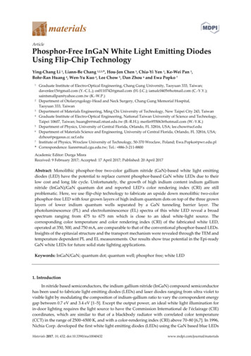
Transcription
ArticlePhosphor-Free InGaN White Light Emitting DiodesUsing Flip-Chip TechnologyYing-Chang Li 1, Liann-Be Chang 1,2,3,*, Hou-Jen Chen 1, Chia-Yi Yen 1, Ke-Wei Pan 1,Bohr-Ran Huang 4, Wen-Yu Kuo 4, Lee Chow 5, Dan Zhou 6 and Ewa Popko 7Graduate Institute of Electro-Optical Engineering, Chang Gung University, Taoyuan 333, Taiwan;davenlee15@gmail.com (Y.-C.L.); os0110742@gmail.com (H.-J.C.); iamalc0405@hotmail.com (C.-Y.Y.);saintsmallpan@yahoo.com.tw (K.-W.P.)2 Department of Otolaryngology-Head and Neck Surgery, Chang Gung Memorial Hospital,Taoyuan 333, Taiwan3 Department of Materials Engineering, Ming Chi University of Technology, New Taipei City 243, Taiwan4 Graduate Institute of Electro-Optical Engineering, National Taiwan University of Science and Technology,Taipei 10607, Taiwan; huangbr@mail.ntust.edu.tw (B.-R.H.); merlin955063@hotmail.com (W.-Y.K.)5 Department of Physics, University of Central Florida, Orlando, FL 32816, USA; lee.chow@ucf.edu6 Department of Materials Science and Engineering, University of Central Florida, Orlando, FL 32816, USA;dzhou@pegasus.cc.ucf.edu7 Institute of Physics, Wroclaw University of Technology, 50-370 Wroclaw, Poland; Ewa.Popko@pwr.edu.pl* Correspondence: liann@mail.cgu.edu.tw; Tel.: 886-3-211-88001Academic Editor: Durga MisraReceived: 9 February 2017; Accepted: 17 April 2017; Published: 20 April 2017Abstract: Monolithic phosphor-free two-color gallium nitride (GaN)-based white light emittingdiodes (LED) have the potential to replace current phosphor-based GaN white LEDs due to theirlow cost and long life cycle. Unfortunately, the growth of high indium content indium galliumnitride (InGaN)/GaN quantum dot and reported LED’s color rendering index (CRI) are stillproblematic. Here, we use flip-chip technology to fabricate an upside down monolithic two-colorphosphor-free LED with four grown layers of high indium quantum dots on top of the three grownlayers of lower indium quantum wells separated by a GaN tunneling barrier layer. Thephotoluminescence (PL) and electroluminescence (EL) spectra of this white LED reveal a broadspectrum ranging from 475 to 675 nm which is close to an ideal white-light source. Thecorresponding color temperature and color rendering index (CRI) of the fabricated white LED,operated at 350, 500, and 750 mA, are comparable to that of the conventional phosphor-based LEDs.Insights of the epitaxial structure and the transport mechanism were revealed through the TEM andtemperature dependent PL and EL measurements. Our results show true potential in the Epi-readyGaN white LEDs for future solid state lighting applications.Keywords: InGaN/GaN; quantum dot; quantum well; phosphor free; white LED1. IntroductionIn nitride based semiconductors, the indium gallium nitride (InGaN) compound semiconductorhas been used to fabricate light emitting diodes (LEDs) and laser diodes ranging from ultra violet tovisible light by modulating the composition of indium-gallium ratio to vary the correspondent energygap between 0.7 eV and 3.4 eV [1–5]. Except the output power, an ideal white light illumination forin-door lighting requires the light source to have the Commission International de l’éclairage (CIE)coordinates, which are similar to that of a blackbody radiator with correlated color temperature(CCT) in the range of 2500–6500 K, and with a color-rendering index (CRI) above 70–80 [6,7]. In 1996,Nichia Corp. developed the first white light emitting diodes (LEDs) using the GaN based blue LEDsMaterials 2017, 10, 432; ls
Materials 2017, 10, 4322 of 11and yellow yttrium aluminum garnet (YAG) phosphor. At present, most of the mature white LEDsare still based on the blue InGaN chips coupled with the yellow-emitting YAG phosphor. Althoughthis technology has been widely adopted in commercial white LEDs, extra costs have resulted fromthe high reaction temperature (over 1800 C) and the high pressure required for synthesizingphosphors, which is a critical drawback. Many other sulfides and fluoride phosphors [8,9] have alsobeen considered, however, poor moisture resistance and the drop in light intensity of these materialslimit their practical applications. To date, sustaining a constant luminous efficiency and CRI value ofthe phosphor-based white LEDs (WLEDs) are still major objectives for the LED industry. Manyresearch groups aimed to develop a gallium nitride (GaN)-based phosphor-free white LED utilizingtwo-color InGaN quantum structures, which we discuss below.In 2001, Damilano et al. [10] demonstrated molecular beam epitaxy (MBE) fabricated monolithic,phosphor-free, white LED wafers with a stack of InGaN/GaN quantum structures, and their lowoutput power electroluminescence (EL) emitted dual wavelengths for the first time. Since then,various groups have fabricated monolithic phosphor free white LEDs [11–13]. For example,Huang et al. [11] used a pre-strained metal organic chemical vapor deposition (MOCVD) techniqueto grow yellow emitting InGaN/GaN quantum structures with increasing Indium concentrations,then, by adding a blue emitting quantum well (QW) at the top of the pre-strained layer, they wereable to fabricate monolithic white LEDs with a color temperature of 5600 K by on-wafer probing.Later, Liu et al. [12] also fabricated dual wavelength InGaN/GaN multiple quantum well-wafers bythe MOCVD method. However, they only reported their photoluminescence (PL) properties at highindium concentrations, and the internal quantum efficiency drops rapidly. Recently, Chi et al. [13]demonstrated a GaN-based two color LED with a p-type insertion layer to control the intensity ratioof two-color emission and also prevented the inter transition. However, despite all the researchefforts, precise process control is still needed to extract the light out of the blue quantum layer, andthis is a problem for the practical commercial application. We should mention briefly here that,recently, Zetian Mi et al. demonstrated a high output power phosphor-free nanowire WLED with anunprecedentedly high CRI of 92–98 [14] and then successfully enhanced the electrical and opticalproperties by fabricating a phosphor-free tunnel junction nanowire WLED [15,16]. That is a topic foranother time.In the field of industrial compound semiconductor epitaxial growth, the lattice mismatchbetween different growth layers with different composite materials can lead to strain or stress, andthe release of this strain or stress can cause phase separation [17,18]. In recent years, lattice relaxationhas been used to control the precipitation of indium in the GaN/InGaN quantum wells, therebyenabling the emitted light to change from green to a longer wavelength, or even to produce indiumrich clusters of epitaxial wafers [19]. These quantum dots exist in the GaN/InGaN QW interfaces [20].For this reason, many attempts have been made recently to replace the phosphor-based LEDs [21,22]with the phosphor-free white LEDs [23]. It is known that the blue band gap quantum wells aretransparent to the green-yellow light emitted from the green-yellow quantum dots (QDs). Thus, thegreen-yellow QD layers should be the first epitaxial layer (on the bottom), followed by the blue QWlayer (on the top). Unfortunately, this tandem structure is very difficult to grow at present, since thehigh indium composition QD layers encounter many problems such as phase separation, dislocation,and extended defects. These problems will prevent the high quality epitaxial growth of the blue QWlayer and will cause the completed two-color tandem structure to have a poor light emittingefficiency. This is attributed to the dislocations and defects induced by the large lattice mismatchbetween the lattices of indium rich InxGa1-xN and GaN, which act as non-radiative recombinationcenters, and, thus, weaken the internal quantum efficiency [24]. These obstacles are often encounteredin the production of QD/QW white LEDs and have resulted in a few reports in the literature on theGaN-based phosphor-free white LEDs. Furthermore, the low CRI value during high currentoperation is another serious problem for the GaN-based phosphor-free white LED. At high currentoperation, the n-side QD ground state transition will be saturated at first, and the blue QW groundstate transition, as well as the blue QW to green-yellow QD tunneling transition, will increase. In theend, the blue light emission will dominate the output spectrum and will cause a low CRI value.
Materials 2017, 10, 4323 of 11In this work, to realize the high CRI phosphor-free white LEDs, a tandem structure is proposed.It includes low indium ratio blue QW layers on the bottom, high indium ratio green-yellow QD layerson the top to improve epitaxial growth, together with a thick tunnel barrier (TB) layer to prevent theQW-QD coupling transitions; see Figure 1a,b. After the epitaxial growth, the phosphor-free WLEDwas processed and fabricated into chips. We applied a thermal sonic flip chip (FC) bondingtechnology, as shown in Figure 1c,d, to bond the fabricated phosphor-free white LED chip to a siliconsub-mount [25–29], which acted as a heat sink. After the FC processing, the green-yellow QD is onthe bottom, the blue QW is the top, and the emitted green-yellow light from the QD can easilypenetrate the top blue QW layers and produce a high CRI value of 82, even under the elevated currentoperation conditions of 350–700 mA. Current-voltage (I–V) measurements, electroluminescent sphereintegration measurements, and temperature variation photoluminescence spectroscopy have beencarried out to investigate the correspondent optical and electrical properties of the fabricatedphosphor-free QW/QD white LED in the following text.Figure 1. (a) The schematic diagram of the white light emitting diode (LED) samples based on indiumgallium nitride (InGaN) QDs and QWs; (b) A thick tunneling block layer was inserted between QDand QW layers; (c) The schematic diagram of the QD/QW white LEDs with flip-chip mounting;(d) The picture of fabricated QD/QW white LED after the flip chip (FC) process.2. ExperimentsThe proposed two-color phosphor-free white light epitaxial wafer with a thick TB layer used forfabricating phosphor-free white LEDs were grown at A-STAR Singapore using a metal organicchemical vapor deposition system (MOCVD). The technologies of high-efficiency InGaN/GaNQW-based blue LEDs are quite mature and these LEDs are commercially available [30]. However,many arduous challenges to improve the performance of the green-yellow LEDs still exist [31]. Themost difficult part is the large lattice mismatch (11%) between the GaN and indium nitride (InN). Theincrease in indium content becomes difficult owing to the miscibility among these binary or ternarycompounds. Therefore, in this work, we start with the epitaxial growth of QW first, then grow thethick TB layer, and finally deposit the high indium ratio green-yellow light emitting QD layers [32].The LED structure layers were grown on a C-oriented (0001) 2-inch-diameter sapphire substrate.After the thermal annealing process, all samples consisted of a 25 nm GaN buffer, 1.2 μm undopedGaN, and 1.5 μm graded doped n-GaN layer. Then, three layers of QW, a 11.8 nm TB layer, and four
Materials 2017, 10, 4324 of 11layers of green-yellow QD structure were deposited. Here, the QW layers consisted of In0.19Ga0.81N(blue) and In0.23Ga0.77N (green) structures and the QD layers consist of different aggregate sizes.To prevent the continuing growth of the green-yellow QW/QD layer and blue QW layer that wasseen previously [33], we have grown a thick 11.8 nm block layer in between the blue QW and greenyellow QW/QD layers to prevent inter-transition. Finally, a thick p GaN layer was grown on top ofthe QD/QW grown layer. After the epitaxial growth, a low temperature thermal activation processwas performed. Then, a chip with dimensions of 1 1 mm2 was fabricated by the standard process oflateral contact electrodes. A 300-nm-thick indium-tin-oxide (ITO) film, used as the current spreadinglayer, was deposited by electron-beam evaporation, and the Cr/Pt/Au metal films were used as then- and p bonding pad contacts. These white LED processes and the subsequent FC package processeswere carried out in the LED fabrication facility at the Green Technology Research Center of ChangGung University. We used the FC technology with gold bumps as the heat dissipation path to enhanceboth the light mixing property and the cooling capacity of the fabricated QD/QW white LED [29].The TEM samples were prepared by using the focused ion beam (FIB, FEI FIB200) system witha 30 kV Gallium liquid metal ion source and the scanning transmission electron microscope(STEM)/TEM analysis was carried out by employing the FEI Tecnai F30 TEM with a field emissionelectron filament operated at 300 kV. Both FIB and STEM works were carried out at the University ofCentral Florida.For the PL temperature dependent experiments, the sample was placed in a continuous flowliquid helium cryostat and experiments were performed by using a HeCd laser with a wavelength of325 nm. The EL in the temperature investigation was detected using a photometric integrating sphere.The samples were mounted on a substrate of aluminum-copper alloy, and then fixed on the hotplateby using thermos paste. The thermocouple probe was pasted on the edge of the LED module formaintaining the temperature from 50 to 170 C.3. Results and Discussion3.1. Characterizations of the QD/QW StructureAfter the epitaxial growth, to acquire an overall image of the grown structure, the TEM samplewas prepared by the FIB, and images are shown in Figure 2. Before the FIB-TEM sample preparation,the Pt bar was deposited as an ion mask, as shown in Figure 2a. After the FIB ion etching, we used atungsten needle to lift out the selected section from the epitaxial growth wafer, as show in Figure 2b.Next, the thin FIB sample section was mounted on a TEM grid, then the final step was to further thinand polish the selected section, as shown in Figure 2c.A STEM image at low magnification was obtained, and the corresponding growth of the QD/QWwere about 800 nm below the top surface, as shown in Figure 2d. The STEM images revealed fourlayers of the green-yellow QD structure on top of the three layers of the blue QW structure, whichare shown in Figure 2e,f with different magnifications. As we demonstrated in Figure 1a, the lowindium ratio blue QW layers were grown first and then were followed by the high indiumgreen-yellow QD layers, which makes the epitaxial growth of this tandem structure much easier thanthe opposite tandem structure [34]. Measured from the TEM images, the thickness of the barriersbetween the QDs and the QWs were about 4.4 and 6.2 nm, respectively. As we proposed, a 11.8 nmTB layer was grown in between the QD and the QW layers to prevent coupling transitions from theQW to the QD [35]. In our previous study, the InGaN/GaN superlattices were helpful to improve theindium composition in the InGaN QDs [5].Figure 3a shows the temperature dependent PL spectra from 50 to 300 K. Figure 3b presents thePL spectrum of a QD/QW wafer at a temperature 20 K and the side peak which was decomposed intoseveral sub peaks. The incongruency of the observed peaks in Figure 3a and the sub peaks in Figure3b are attributed to the non-uniform epitaxial growth of the QDs. Figure 3c,d summarizes thetemperature dependency wavelengths of PL peaks 1 and peak 3, respectively. The total shifts of thePL peaks 1 and 3 from 50 to 400 K are 2 and 3 meV, respectively. These shifts are all less than 5 meV,while those shifts in the InGaN bulk are more than 30 meV, as reported in the literature [36]. In a
Materials 2017, 10, 4325 of 11previous report of the PL properties of the InGaN/GaN QDs [37], as the temperature increases,carriers can be thermally transferred into low-energy states from high-energy states. The small shiftobserved in our samples may be due to a similar effect.Figure 2. (a) FIB-TEM sample preparation, selective area, and deposit Pt bar; (b) After FIB etching,using a W needle to lift out the section; (c) Thin FIB sample section mounted on a TEM sample gridand further thinning and polishing of the processed section; (d) An overall STEM image at lowmagnification, QD/QW structures are about 800 nm deep to the surface; (e,f) The STEM images athigh magnification with four QD structures on top and three QW layers at the bottom areclearly observed.Figure 3. (a) The temperature dependent photoluminescence (PL) spectra from 50 to 300 K; (b) The PLspectrum of a grown QD/QW wafer at temperature 20 K, and the decomposed sub peaks from the PLspectrum by using a software Origin 8.1; (c) the PL peak 1 spectra of the cool white QD LEDs withvaried temperature from 50 to 400 K; (d) the PL peak 3 spectra of the cool white QD LEDs with variedtemperature from 50 to 400 K.
Materials 2017, 10, 4326 of 113.2. Device Characterization of QD/QW LEDsFigure 4a shows the room temperature current voltage (IV) curves. At the forward bias, the turn-onvoltage of the fabricated QD/QW WLED is approximately 2.8 V, with a standard injected current of350 mA. The slope of its IV curve is larger than the commercial ones, which implies an excessiveseries resistance. This excess resistance is thought to be due to the stack structure itself, whichincludes a high concentration of grown defects accompanied with the QD formation process and theextra FC packaging process as well. After close examination of the leakage current at the reverse bias,it was revealed that the leakage current of the QD/QW WLED under a reverse bias of 2.5 V wasalmost 1 μA and was thought to be due to the reverse tunneling current from the high concentrationdefects of the Indium (In) rich grown layers [38,39].In efficient, QW, LED electroluminescence, the majority of the injected electrons and holesshould be converted into photons through radiative recombination. However, in most QD LEDworks, they were converted into phonons via non-radiative recombination and are eventuallytransferred to heat. This is the reason why a direct observation of the EL emission in the GaN basedQD/QW white LED is difficult. In this work, Figure 4b shows the temperature dependent EL spectraof the white QD LEDs under 350 mA injection current from 50 C to 170 C, and Figure 4c successfullydisplays the temperature dependent EL spectra from 50 C to 170 C, respectively. In this figure, thebroad EL spectra, with the wavelength extending from 475 nm to 675 nm, and a broad peak centeredat 570 nm are shown, which is close to the ideal wavelength range of a white-light source. However,some noise peaks were occasionally found during the EL measurement for devices picked from thesame growth wafer, which indicates that the fabricated white LEDs exhibited not only the latticemismatch induced defects, but also the non-uniform QD distributions which are also consistent withthe large leakage current phenomenon of IV curves.As the temperature increases, a decrease of their intensity is due to both the carrier overflow andthe vibrations in the lattice as the temperature rises, which decrease the probability of a radiativerecombination and increases the probability of a non-radiative recombination. At the QD/QW whiteLEDs’ EL spectra, the changes in the peak wavelength can be categorized in terms of the twotemperature zones. The first zone lies between 50 C and 70 C, where a blue shift of the main peakfrom 593 nm to 585 nm takes place. This result may be attributed to the suppression of the quantumconfinement Stark effect [40]. The second zone lies between 70 C and 170 C, where the main peakdisplays a steady red shift from 585 nm to 593 nm which is caused by the lattice expansion andvibration [41]. Nevertheless, a low power output was determined from the EL measurements, whichcan also be attributed to the inferior crystalline quality of the QD, due to its highly dense andunfavorable composition in the InGaN QD layers, and a further study of the epitaxial growthconditions is needed [33,42].
Materials 2017, 10, 4327 of 11Figure 4. (a) The current voltage (IV) curves of the white QD LEDs at room temperature; (b)The temperature dependent electroluminescence (EL) spectra of the white QD LEDs at 50 C–170 C.;(c) The temperature dependent EL peak intensity and wavelength at 350 mA.3.3. Light Mixing PropertiesAfter the FC package, the FC devices were checked by a probe station with a bias current of50 mA to obtain a clear picture of these devices with bonding pads. The QD/QW white LED is shownin Figure 5a. The blue, cold, white output light was obtained, which is due to the fact that the electronhas a higher mobility than a hole, and it dominates the light sequence, which is injected from thebottom n-side to the low indium QW layer to emit a blue light first. Thus, a short wavelength bluelight emits through the sapphire substrate. As the bias current increased to 350 mA, the injectedelectrons go deeper into the green-yellow QD layer and the output becomes brighter, as shown inFigure 5b. Finally, at 500 mA, the long wavelength QD layer emits a green-yellow light mixed with ablue light, forming a warm white light as shown in Figure 5c. By mixing the emission lights from theQDs and QWs, the fabricated QD/QW white LED emits a warm white light, as the photos show inFigure 5c. We applied various bias currents of 350 mA, 500 mA, and 700 mA to the FC QD/QW whiteLED, and used an integrating sphere to measure its correspondent color temperature and CRI.Table 1 presents the luminous efficacy of the QD-LED at the different bias currents. At its peak,the luminous efficacy was about 0.0024 lm/W at 350 mA, which is considerably lower than the value70 100 lm/W of common LEDs.Table 1. Luminous efficacy of white QD-LED at 350, 500 and 700 mA. CIE stands for CommissionInternational de l’éclairage.Set Current Value(mA)350500700Relative Color Temperature(K)512651303994CIE xCIE 570.25Color Purity(%)14.1713.8167.99Figure 5d–f demonstrates the QD/QW white LEDs’ chromaticity diagrams of the color spaceresulting from the different bias currents of 350, 500 and 700 mA, respectively. At the QW/QD tandemsystem, coupling probability between the QW ground state and the QD ground state is inverselyproportionate to the thickness of the tunneling block layer. Thus, in our design, a 12 nm TB layer wasinserted in between the QD and QW layers to prevent the tunneling transition taking place, whichmakes the emitted blue light dominate and decreases the CRI value considerably [33]. As shown inFigure 5d,f, QD white LED’s color temperature and the CRI at the bias currents of 350 and 500 mAreached 5126 and 5130 K, 82 and 83.4, respectively. These values are good enough in comparison tothe conventional phosphor-based LED, which has a color temperature of 4500 K and a CRI value of75. In addition, these values are much better than a recent report with a CRI value as low as 13, inwhich a reverse tandem QW/QD white LED structure without a TB layer had been fabricated [33].
Materials 2017, 10, 4328 of 11Here, we report the color temperature and the CRI still have good values of 3994 K and 70,respectively, even as the bias current is increased to a value as high as 700 mA.In the current dependent thermal measurement, we observed that under a 350 mA operation,the junction temperature of our WLED is approximately 120 C, whereas at the 700 mA operation,the junction temperature reaches as high as 200 C. Table A1 presents the CRI test of the white LEDaccording to DIN 6169 at the 350, 500 and 700 mA operation, respectively. The corresponding CRIdecreased from 82 to around 70, when the current increased from 350 mA to 700 mA because the redlight performance index of R9 dropped from 40 to 35. The reduced red band observed at 200 C alsocontributed to the blue shift.Figure 5. (a) The images of the FC package QD/QW cool white LED driven at 5 mA; (b) The imagesof the light outputs from QD/QW white LEDs were taken as the current increased to 50 mA. The colortemperatures and color coordinates of color rendering of white QD/QW LEDs at different biascurrents of (c) 350 mA; (d) 500 mA; and (e) 700 mA.4. ConclusionsThe fabrication of a phosphor-free long-wavelength-top tandem cell QD/QW cool white LEDwas accomplished by MOCVD epitaxial growth followed by flip-chip technology. Because FCtechnology is applied, the grown sequence can be arranged with the low Indium (In) ratio layers firstand the high In ratio layers second, which makes the epitaxial process easier. That also means the4-layers of In-rich QD structure are grown on top of the 3-layers of low In blue QW structure. Afterthe flip chip process, the conventional epitaxial growth that results in a blue light absorption problemin the high In ratio layer was then solved. In addition, with conventional QD/QW tandem structures,those layers are grown continuously with a thin block layer or without a block layer which results ina low CRI during high current operation. In this work, the QD/QW inter transition problem wassolved by inserting a 11.8 nm TB layer. The successful EL exhibited a distribution of the emissionspectrum that varied from 450 to 700 nm, which is very close to the ideal white-light source and iswider than that of the phosphor-based white LEDs. At a standard bias current of 350 mA, a colortemperature of 5126 K, and a CRI value of 82.17, are presented, which is better than the recentlyreported results with a reverse epitaxial structure.However, those single-chip QW/QD cool white LEDs have an unexpected drawback of lowluminous efficiency. The requirement of overall luminous efficiency of QW/QD LEDs can beimproved by optimizing the thickness, growth conditions, and the concentration of dopant in theQW and QD layers. Furthermore, the thickness of the TB layer might have reduced the efficiencymore than expected due to its increased resistance. These factors present an important basis for thefabrication of single-chip white LEDs. Thus, an efficient phosphor-free white InGaN based LEDrequires more time and research.
Materials 2017, 10, 4329 of 11Acknowledgments: This work was financially supported by the National Science Council (NSC), Taiwan,currently known as Ministry of Science and Technology (MOST) under contract No. NSC-101-2221-E-182-047MY2, and the partial support from NCBiR (Polish National Center for Research and Development) project No.PL-TW/1/2013/23 is also appreciated.Author Contributions: Liann-Be Chang was the originator of the idea of this study and conceived most of theexperiments; Dan Zhou and Lee Chow were responsible for the FIB and TEM analysis; Ying-Chang Li,Hou-Jen Chen, Chia-Yi Yen, Ke-Wei Pan, Bohr-Ran Huang, and Wen-Yu Kuo performed the experiments andsample characterizations. Ewa Popko was responsible for the data analysis and discussion. Ying-Chang Li wrotethe manuscript under the supervision of Liann-Be Chang and Lee Chow. All the authors have together discussedand interpreted the results. All the authors read the final manuscript.Conflicts of Interest: The authors declare no conflict of interest.Appendix ATable A1. The 14 CRI test colors of FC package QD/QW WLED according to DIN 6169 at the biascurrents of 350, 500 and 700 mA.Bias CurrentR1R2R3R4R5R6R7R8R9R10R11R12R13R14Ra350 7581387.062782.17872500 0125887.5231183.41642700 1.6981455.46916 3745References1.2.3.4.5.6.7.Mohammad, S.N.; Salvador, A.A.; Morkoc, H. Emerging Gallium Nitride Based Devices. Proc. IEEE 1995,83, 1306–1355.Nakamura, S.; Senoh, M.; Nagahama, S.I.; Iwasa, N.; Yamada, T.; Matsushita, T.; Kiyoku, H.; Sugimoto, Y.;Kozaki, T.; Umemoto, H.; et al. InGaN/GaN/AlGaN-Based Laser Diodes with Modulation-DopedStrained-Layer Superlattices Grown on an Epitaxially Laterally Overgrown GaN Substrate. Appl. Phys. Lett.1998, 72, 211–213.Muthu, S.; Gaines, J. Red, Green and Blue LED-Based White Light Source: Implementation Challenges andControl Design. In Proceedings of the 38th IAS Annual Meeting: Crossroads to Innovation, 2003 IEEEIndustry Applications Conference, Salt Lake City, UT, USA, 12–16 October 2003; pp. 515–522.Chang, L.B.; Chang, Y.H.; Jeng, M.J. Light Output Improvement of InGaN-based light-Emitting Diodes byMicrochannel Structure. IEEE Photonics Technol. Lett. 2007, 19, 1175–1177.Lai, M.J.; Jeng, M.J.; Chang, L.B. High-Efficiency InGaN-Based Yellow-Green Light-Emitting Diodes.Jpn. J. Appl. Phys. 2010, 49, 021004.Brinkley, S.E.; Pfaff, N.; Denault, K.A.; Zhang, Z.; Hintzen, H.T.; Seshadri, R.; Nakamura, S.; DenBaars, S.P.Robust Thermal Performance of Sr2Si5N8:Eu2 : An efficient red emitting phosphor for light emitting diodebased white lighting. Appl. Phys. Lett. 2011, 99, 241106.Oh, J.H.; Oh, J.R.; Park, H.K.; Sung, Y.-G.; Do, Y.R. Highly-Efficient, Tunable Green, Phosphor-ConvertedLEDs Using a Long-Pass Dichroic Filter and a Series of Orthosilicate Phosphors for Tri-Color White LEDs.Opt. Express 2011, 19, 4188–4198.
Materials 2017, 10, 4.25.26.27.10 of 11Setlur, A.A.; Radkov, E.V.; Henderson, C.S.; Her, J.-H.; Srivastava, A.M.; Karkada, N.; Kishore, M.S.;Kumar, N.P.; Aesram, D.; Deshpande, A.; et al. Energy-Efficient, High-Color-Rendering LED Lamps UsingOxyfluoride and Fluoride Phosphors. Chem. Mater. 2010, 22, 4076–4082.Kuo, T.-W.; Liu, W.-R.; Chen, T.-M. High Color Rendering White Light-Emitting-Diode Illuminator Usingthe Red-Emitting Eu2 -Activated CaZnOS Phosphors Excited by Blue LED Available. Opt. Express 2010, 18,8187–8192.Damilano, B.; Grandjean, N.; Pernot, C.; Massies, J. Monolith
Nichia Corp. developed the first white light emitting diodes (LEDs) using the GaN based blue LEDs Materials 2017 , 10 , 432 2