Transcription
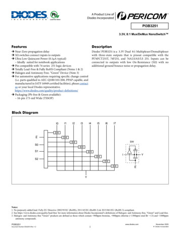
PbA Product Line ofDiodes IncorporatedLead-free GreenPI3B32513.3V, 8:1 Mux/DeMux NanoSwitch FeaturesDescription¼¼Near-Zero propagation delay¼¼5Ω switches connect inputs to outputs¼¼Ultra Low Quiescent Power (0.1µA typical)– Ideally suited for notebook applications¼¼Pin compatible with 74 series 251 logic devices¼¼Totally Lead-Free & Fully RoHS Compliant (Notes 1 & 2)¼¼Halogen and Antimony Free. “Green” Device (Note 3)¼¼For automotive applications requiring specific change control(i.e. parts qualified to AEC-Q100/101/200, PPAP capable, andmanufactured in IATF 16949 certified facilities), please contactus or your local Diodes uct-definitions/¼¼Packaging (Pb-free & Green available):– 16-pin 173-mil Wide (TSSOP)Diodes' PI3B3251 is a 3.3V Dual 8:1 Multiplexer/Demultiplexerwith three-state outputs that is pinout compatible with thePI74FCT251T, 74F251, and 74ALS/AS/LS 251. Inputs can beconnected to outputs with low On-Resistance (5Ω) with noadditional ground bounce noise or propagation delay.Block EYNotes:1. No purposely added lead. Fully EU Directive 2002/95/EC (RoHS), 2011/65/EU (RoHS 2) & 2015/863/EU (RoHS 3) compliant.2. See https://www.diodes.com/quality/lead-free/ for more information about Diodes Incorporated’s definitions of Halogen- and Antimony-free, "Green" and Lead-free.3. Halogen- and Antimony-free "Green” products are defined as those which contain 900ppm bromine, 900ppm chlorine ( 1500ppm total Br Cl) and 1000ppmantimony compounds.PI3B3251Document Number DS42816 Rev 1-21www.diodes.comNovember 2020Diodes Incorporated
A Product Line ofDiodes IncorporatedPI3B3251Pin 611S0E710S1GND89S2Pin DescriptionPin#Pin NameDescription4, 3, 2, 1, 15, 14, 13, 12I0–7Data Inputs11, 10, 9S0–2Select Inputs7EEnable5YData Outputs8GNDGround16VCCPower6NCNo ConnectTruth Table(1)ESelectYFunctionXHi-ZDisableLLI0S2-0 0LLHI1S2-0 1LLHLI2S2-0 2LLHHI3S2-0 3LHLLI4S2-0 4LHLHI5S2-0 5LHHLI6S2-0 6LHHHI7S2-0 7S2S1S0HXXLLLNote:1. H High Voltage Level, L Low Voltage LevelPI3B3251Document Number DS42816 Rev 1-22www.diodes.comNovember 2020Diodes Incorporated
A Product Line ofDiodes IncorporatedPI3B3251Maximum Ratings(Above which the useful life may be impaired. For user guidelines, not tested.)Storage Temperature. –65 C to 150 CAmbient Temperature with Power Applied. –40 C to 85 CSupply Voltage to Ground Potential . –0.5V to 4.6VDC Input Voltage.–0.5V to 4.6VDC Output Current. 120mAPower Dissipation. 0.5WNote:Stresses greater than those listed under MAXIMUMRATINGS may cause permanent damage to thedevice. This is a stress rating only and functionaloperation of the device at these or any other conditions above those indicated in the operational sections of this specification is not implied. Exposureto absolute maximum rating conditions for extendedperiods may affect reliability.DC Electrical Characteristics (Over the Operating Range, TA –40 C to 85 C, VCC 3.3V 10%)ParametersDescriptionTest Conditions(1)Typ(2)Min.Max.VIHInput HIGH VoltageGuaranteed Logic HIGH Level2.0VILInput LOW VoltageGuaranteed Logic LOW Level–0.5IIHInput HIGH CurrentVCC Max., VIN VCC 1IILInput LOW CurrentVCC Max., VIN GND 1IOZHHigh Impedance Output Current0 IN, Y VCC 1VIKClamp Diode VoltageVCC Min., IIN –18mARONSwitch On-Resistance(3)UnitsV0.8µA–1.2VCC Min., VIN 0.0V,ION 48mA or 64mA58VCC Min., VIN 2.4V,ION 15mA1017VΩNotes:1.For Max. or Min. conditions, use appropriate value specified under Electrical Characteristics for the applicable device type.2.Typical values are at VCC 3.3V, Ta 25 C ambient and maximum loading.3.Measured by the voltage drop between I and Y pin at indicated current through the switch. On-Resistance is determined by the lower of the voltages on the two(I,Y) pins.Capacitance (TA 25 C, f 1 MHz)Parameters(1)DescriptionCINInput CapacitanceCI(OFF)I0 - I7 Capacitance, Switch OffCY(OFF)Y Capacitance, Switch OffCI(ON)I0 - I7 Capacitance, Switch OnTest ConditionsTyp.Units3.0VIN 0V8.064.0pF72.0Note:1.This parameter is determined by device characterization but is not production tested.PI3B3251Document Number DS42816 Rev 1-23www.diodes.comNovember 2020Diodes Incorporated
A Product Line ofDiodes IncorporatedPI3B3251Power Supply CharacteristicsParametersTest Conditions(1)DescriptionICCQuiescent Power Supply Current VCC Max.VIN GND or VCCΔIccSupply Current per Input@ TTL HIGHVIN 3.0V(3)VCC Max.Min.Typ.(2)Max.0.13750UnitsµANotes:1. For Max. or Min. conditions, use appropriate value specified under Electrical Characteristics for the applicable device.2. Typical values are at VCC 3.3V, 25 C ambient.3. Per TTL driven input (control input only); I and Y pins do not contribute to ICC.Switching Characteristics over Operating opagation Delay(1,2), In to YBus Enable Time, Sn to YBus Enable Time, E to YConditionsCL 50pFRL 500ΩBus Disable Time, E to YCom.Min.1Max.0.254.513.515.5UnitsnsNotes:1.This parameter is guaranteed but not tested on Propagation Delays.2.The bus switch contributes no propagational delay other than the RC delay of the On-Resistance of the switch and the load capacitance. The time constant for theswitch alone is of the order of 0.25ns for 50pF load. Since this time constant is much smaller than the rise/fall times of typical driving signals, it adds very littlepropagational delay to the system. Propagational delay of the bus switch when used in a system is determined by the driving circuit on the driving side of theswitch and its interaction with the load on the driven side.Applications InformationLogic InputsThe logic control inputs can be driven up to 3.6V regardless of the supply voltage. For example, given a 3.3V supply, IN may be drivenlow to 0V and high to 3.6V. Driving IN Rail-to-Rail minimizes power consumption.Power-Supply Sequencing and Hot-Plug InformationProper power-supply sequencing is recommended for all CMOS devices. Always apply VCC and GND before applying signals to input/output or control pins.Rail-to-Rail is a registered trademark of Nippon Motorola, Ltd.Part MarkingPI3B3251LEYYWWGGYYWW: Date Code (Year & Workweek)1st G: Assembly Site Code2nd G: Wafer Fab Site CodePI3B3251Document Number DS42816 Rev 1-24www.diodes.comNovember 2020Diodes Incorporated
A Product Line ofDiodes IncorporatedPI3B3251Packaging Mechanical: 16-TSSOP (L)16-0061For latest package info.please check: haracteristics/Ordering InformationOrdering CodePackage CodePI3B3251LEXLPackage Description16-pin, 173-mil Wide (TSSOP)Notes:1. No purposely added lead. Fully EU Directive 2002/95/EC (RoHS), 2011/65/EU (RoHS 2) & 2015/863/EU (RoHS 3) compliant.2. See https://www.diodes.com/quality/lead-free/ for more information about Diodes Incorporated’s definitions of Halogen- and Antimony-free, "Green" and Lead-free.3. Halogen- and Antimony-free "Green” products are defined as those which contain 900ppm bromine, 900ppm chlorine ( 1500ppm total Br Cl) and 1000ppmantimony compounds.4. E Pb-free and Green5. X suffix Tape/ReelPI3B3251Document Number DS42816 Rev 1-25www.diodes.comNovember 2020Diodes Incorporated
A Product Line ofDiodes IncorporatedPI3B3251IMPORTANT NOTICE1.DIODES INCORPORATED AND ITS SUBSIDIARIES (“DIODES”) MAKE NO WARRANTY OF ANY KIND, EXPRESS OR IMPLIED, WITH REGARDS TOANY INFORMATION CONTAINED IN THIS DOCUMENT, INCLUDING, BUT NOT LIMITED TO, THE IMPLIED WARRANTIES OF MERCHANTABILITY, FITNESS FORA PARTICULAR PURPOSE OR NON-INFRINGEMENT OF THIRD PARTY INTELLECTUAL PROPERTY RIGHTS (AND THEIR EQUIVALENTS UNDER THE LAWSOF ANY JURISDICTION).2.The Information contained herein is for informational purpose only and is provided only to illustrate the operation of Diodes products described herein andapplication examples. Diodes does not assume any liability arising out of the application or use of this document or any product described herein. This document isintended for skilled and technically trained engineering customers and users who design with Diodes products. Diodes products may be used to facilitate safety-relatedapplications; however, in all instances customers and users are responsible for (a) selecting the appropriate Diodes products for their applications, (b) evaluating thesuitability of the Diodes products for their intended applications, (c) ensuring their applications, which incorporate Diodes products, comply the applicable legal andregulatory requirements as well as safety and functional-safety related standards, and (d) ensuring they design with appropriate safeguards (including testing, validation,quality control techniques, redundancy, malfunction prevention, and appropriate treatment for aging degradation) to minimize the risks associated with their applications.3.Diodes assumes no liability for any application-related information, support, assistance or feedback that may be provided by Diodes from time to time. Anycustomer or user of this document or products described herein will assume all risks and liabilities associated with such use, and will hold Diodes and all companieswhose products are represented herein or on Diodes’ websites, harmless against all damages and liabilities.4.Products described herein may be covered by one or more United States, international or foreign patents and pending patent applications. Product namesand markings noted herein may also be covered by one or more United States, international or foreign trademarks and trademark applications. Diodes does not conveyany license under any of its intellectual property rights or the rights of any third parties (including third parties whose products and services may be described in thisdocument or on Diodes’ website) under this document.5.Diodes products are provided subject to Diodes’ Standard Terms and Conditions of Sale nditions/terms-and-conditions-of-sales/) or other applicable terms. This document does not alter or expand the applicable warranties provided by Diodes. Diodes does not warrant or accept any liability whatsoever in respect of any products purchased through unauthorized sales channel.6.Diodes products and technology may not be used for or incorporated into any products or systems whose manufacture, use or sale is prohibited under anyapplicable laws and regulations. Should customers or users use Diodes products in contravention of any applicable laws or regulations, or for any unintended or unauthorized application, customers and users will (a) be solely responsible for any damages, losses or penalties arising in connection therewith or as a result thereof, and(b) indemnify and hold Diodes and its representatives and agents harmless against any and all claims, damages, expenses, and attorney fees arising out of, directly orindirectly, any claim relating to any noncompliance with the applicable laws and regulations, as well as any unintended or unauthorized application.7.While efforts have been made to ensure the information contained in this document is accurate, complete and current, it may contain technical inaccuracies,omissions and typographical errors. Diodes does not warrant that information contained in this document is error-free and Diodes is under no obligation to update orotherwise correct this information. Notwithstanding the foregoing, Diodes reserves the right to make modifications, enhancements, improvements, corrections or otherchanges without further notice to this document and any product described herein. This document is written in English but may be translated into multiple languages forreference. Only the English version of this document is the final and determinative format released by Diodes.8.Any unauthorized copying, modification, distribution, transmission, display or other use of this document (or any portion hereof) is prohibited. Diodes assumes no responsibility for any losses incurred by the customers or users or any third parties arising from any such unauthorized use.Copyright 2020 Diodes Incorporatedwww.diodes.comPI3B3251Document Number DS42816 Rev 1-26www.diodes.comNovember 2020Diodes Incorporated
switch and its interaction with the load on the driven side. Applications Information Logic Inputs The logic control inputs can be driven up to 3.6V regardless of the supply voltage. For example, given a 3.3V supply, IN may be driven low to 0V and high to 3.6V. Driving IN Rail-to-Rail minimizes power consumption.