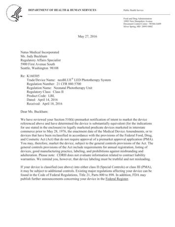
Transcription
ORGANICLIGHT-EMITTING DIODESLIGHTING TOWARD A SUSTAINABLE ENVIRONMENTColleen Cleary (Undergraduate)Leo Panish (HS Student)Angelo Angeles (HS Teacher)Dr. Reginald Eze (Mentor)Dr. Yasser Hassebo (Mentor)1
ObjectiveChanging the parameters of a simulated OLEDand analyzing the effects of these changes onOLED emission pa erns.The results of this study provide a template fora potenAal OLED with enhanced colorbrilliance and brightness.2
ORGANIC LIGHT EMITTING DIODELIGHTING IntroducAon What is an Organic Light-EmiHng Diode? OLEDs Compared to Other Light Sources History and ApplicaAons of Organic LightEmiHng Diodes How Does it Work? Method Results and Conclusion Why is it the Next GeneraAon ofTechnology?3
What is an OLED?OrganicA compound that is carbon-based.Light-Emitting Diode (LED)An electronic device that emits light when anelectrical current is applied to it.4
What is an OLED?h chem01.jpgAn area light source that contains layers of thin,flexible sheets of organic electroluminescent material.5
What is an OLED?h �les/2011/09/UD-OLED2.jpg6
Evolution of nt lampCompact fluorescent lampLinear fluorescent lampLight-EmiHng DiodeOrganic Light-EmiHng Diode17.5 lm/W49-75 lm/W67-110 lm/Wup to 140 lm/W120 lm/WLifespan found from GE 60W bulbs calculated for 3 hrs/dayLifeAme0.9 years7.3 years5.0 years13.7 years36.5 years7
OLEDs vs.h LED EarlyProduct.JPG OLEDs are area sourcesLEDsh p://www.noguge.com/thumbnail/l/ledlights-8.jpeg LEDs are point sources Small enough to be used as Used to backlight LCD TVspixels in a display Modern displays can be less Modern displays can be lessthan 1.5 inches thick andthan 1mm thick and weighweigh less than 35 lbsless than 4.5 lbs Encased in epoxy (plasAccapsule) Can be made flexible8
History of OLEDs 1950’s: André Bernanose observed electroluminescencein organic materials. 1960: MarAn Pope developed a technique to connect anelectric current to organic crystals.h arAn Pope.jpgh 9/EDC-GlowsAcks.jpgh ploads/2012/01/kodak-logo.jpg 1987: Ching W. Tang and Steven Van Slyke at EastmanKodak reported the first small-molecule OLED device.9
Commercialization of OLEDs In 2003, Kodak began integraAng OLED technology withtheir digital cameras.h ony-bravia-xel-1-ultraslim-oled-tv.jpgh p://h er bis 5 megapixel 16 digitalkameras im fokus/kodak d01.jpgh p://h 5/lg-wallpaper-tv.jpg In 2007, Sony announced the XEL-1, the first OLED TV. In 2015, LG unveiled the world's thinnest OLED TV.10
How does an OLED work? PotenAal difference isapplied to the twoelectrodes. Electrons travel fromcathode to anode. Holes recombine withthe electrons in theemissive layer. Energy is released as lightand directed towards thesubstrate.CATHODEEMISSIVE LAYERCONDUCTIVE LAYERANODESUBSTRATE11
ORGANIC LIGHT EMITTING DIODELIGHTING IntroducAon What is an Organic Light-EmiHng Diode? OLEDs Compared to Other Light Sources History and ApplicaAons of Organic LightEmiHng Diodes How Does it Work? Method Results and Conclusion Why is it the Next GeneraAon ofTechnology?14
Refractive Index Property of materials Defined as 𝑛 𝑐/𝑣Low IndexHigh Index Used to determinevalues such asincident angle of the m 𝑡ℎ layerh 5WsXF refracAon.jpg13
Adding Microcavities and DBRsMicrocavityCreates standing wavesthat amplify the light"Microdisplays Based upon Organic Light-emiHng Diodes." IBM Journal of Research and Developmenth arAal transmi ance.gifDBRProduces standing wavesusing phase changeLow IndexHigh Index14
Nine-Step Algorithm2.ConverCng values for calculaCon3.Outer loop for Incident angles( -90 degrees q 90 degrees )4.CalculaCng Refracted anglesand Layers thickness5. CalculaCng the OpCcal admiMance6.Inner loop for Wavelength(Bragg wavelength /- 180)7.CalculaCng Phase factor andCharacterisCc MatrixFirst SimulaAon 𝐃𝐁𝐑 𝐦𝐃𝐁 𝐃𝐁𝐑 𝟏 𝐑 𝟐SUBSTRATEConducCveEmissiveLayerLayerLow indexHigh indexUser input valuesLow indexHigh indexLow indexHigh index1.OLED with DBRs8. CompuCng the TransmiOvity andReflecCvity values9.Graphs15
Validity of CodeLiddell, Heather Mary., and H. G. Jerrard. "Periodic MulAlayers and the Classical Stack." Computeraided Techniques for the Design of MulAlayer Filters. Bristol: A. Hilger, 1981. 14-18. Print.16
Validity of CodeReflectivity vs Wavelength11 Stack5 Stacks9 Stacks13 Stacks0.9Reflectivity 50Wavelength (nm)17
ApproachReflectivity vs Wavelength1Final SimulaAonReflectivity (%) 𝐃𝐁𝐑 𝐦𝐃𝐁𝐑 𝐦 𝟏0.8SUBSTRATEHigh indexLow indexHigh indexLow indexOLED with DBRs and a 0450500550500550Wavelength (nm)Transmission vs Wavelength10.90.8Transmission (%)ConducCveLayerMicrocavityEmissive LayerLow indexHigh indexLow indexHigh index 𝐃𝐁 𝐃𝐁𝐑 𝟏 𝐑 Wavelength (nm)18
Approach Goals:Reflectivity vs Wavelength10.91. Maximum transmissionat Bragg wavelength2. Maximum reflecAon atsurrounding wavelengthsReflectivity 00550500550Wavelength (nm)Transmission vs Wavelength10.9 Parametric study 𝑅 𝑇 1Transmission (%) Focus on small 00450Wavelength (nm)19
ORGANIC LIGHT EMITTING DIODELIGHTING IntroducAon What is an Organic Light-EmiHng Diode? OLEDs Compared to Other Light Sources History and ApplicaAons of Organic LightEmiHng Diodes How Does it Work? Method Results and Conclusion Why is it the Next GeneraAon ofTechnology?22
ResultsChanging the number of DBR stacks above and below thecavity affects transmission.BeforeReflectivity vs Wavelength110.90.90.80.80.70.7Reflectivity (%)Reflectivity 0250300 350 400Wavelength (nm)450Unequal Stacks500550Reflectivity vs Wavelength0100200300400500600Wavelength (nm)Equal Stacks21
ResultsChanging the substrate index affects maximumtransmission.BeforeReflectivity vs 0.30.20.20.10.10150200250300 350 400Wavelength (nm)High Index450Reflectivity vs Wavelength1Reflectivity (%)Reflectivity (%)After5005500150200250300 350 400Wavelength (nm)Low Index45050055022
ResultsChanging the cavity index affects reflecAon pa erns.BeforeReflectivity vs 0.30.20.20.10.10150200250300 350 400Wavelength (nm)450Far from IntegerReflectivity vs Wavelength1Reflectivity (%)Reflectivity (%)After5005500150200250300 350 400Wavelength (nm)450Close to Integer50055023
ResultsChanging the length of the microcavity affectstransmission at the Bragg wavelength.BeforeReflectivity vs 0.30.20.20.10.10150200 1/8250300 350 400Wavelength (nm)450Reflectivity vs Wavelength1Reflectivity (%)Reflectivity (%)After500Bragg wavelength5500150200250300 350 400Wavelength (nm)450BraggWavelength 1/250055024
ConclusionFor Maximum Transmission:3. Cavity refracAve index closeto integer.4. Cavity length of 1/2 or 1/4 theBragg wavelength.0.90.8Reflectivity (%)2. Substrate refracAve indexclose to 1.0 (vacuum).Reflectivity vs 0450500550500550Wavelength (nm)Transmission vs Wavelength10.90.8Transmission (%)1. Equal DBR stacks aboveand below 00Wavelength (nm)45025
ORGANIC LIGHT EMITTING DIODELIGHTING IntroducAon What is an Organic Light-EmiHng Diode? OLEDs Compared to Other Light Sources History and ApplicaAons of Organic LightEmiHng Diodes How Does it Work? Method Results and Conclusion Why is it the Next GeneraAon ofTechnology?28
Organic Light-Emitting DiodesADVANTAGES Energy efficient Environmentally friendly Does not emit heat or UVrays Closest light source tonatural light Thinner and lighter thanother light sources Cost decrease predicted tooccur in the next 5 years Can be produced as largesheets Truer blacks and be ercontrast on displaysDISADVANTAGES Efficiency is sAll lowcompared to LED efficiency Blue OLED lifeAme is muchshorter than the red andgreen The cost to manufacture iscurrently expensive SensiAve to water and UVrays27
Potential OLED Applicationsh p://www.superimaging.com/img/hud1.jpgh /objects/news/6/7/10/GECIA -touchscreen-walls-cpi-6.jpg28
1.2.3.4.5.6.7.8.9.10.11.12.13.14.SourcesHeavens, O. S. OpAcal ProperAes of Thin Solid Films. London: Bu erworths ScienAfic PublicaAons,1955. Print.Geffroy, Bernard, Philippe Le Roy, and Christophe Prat. "Organic Light-emiHng Diode (OLED)Technology: Materials, Devices and Display Technologies." Polym. Int. Polymer Interna.onal 55.6(2006): 572-82. Print.Kalyani, N. Thejo, and S.j. Dhoble. "Organic Light EmiHng Diodes: Energy Saving LighAng Technology—A Review." Renewable and Sustainable Energy Reviews 16 (2012): 2696-723. Print"OLED Technology: IntroducAon and Basics." OLED Technology: Introduc.on and Basics. Web. 6 July2015.Howard, W. E., and O. F. Prache. "Microdisplays Based upon Organic Light-emiHng Diodes." IBMJournal of Research and Development IBM J. Res. & Dev. (2001): 115-27. Print.Burroughes, J.H. "Light-emiHng Diodes Based on Conjugated Polymers." Nature 347 (1990): 352. PrintAntoniadis, Homer, Ph.D. "Overview of OLED Display Technology." Osram OpAcal Semiconductors.h 1a.pdf"DuPont shows new AMOLED materials and OLED displays" OLED-Info.com.Howard, Webster E. "Be er Displays with Organic Films." Sci Am ScienAfic American (2004): 76-81.Print."Kodak Unveils World's First Digital Camera with OLED Display" Eastman Kodak. 3/2/2003.Michael J. Felton (2001) "Thinner lighter be er brighter, Today's Chemist at Work."; 10 (11): 30-34Williams, Martyn. "PC World - Sony Readies OLED TV".4/12/2007.Reisinger, Don. "LG Display Shows off Press-on 'wallpaper' TV under 1mm Thick - CNET." CNET. 19 May2015. Web. 6 July 2015.Schubert, E. Fred. “Light EmiHng Diodes and Solid-State LighAng.” Light EmiHng Diodes29
AcknowledgementsNaAonal AeronauAcs and Space AdministraAon (NASA)NASA Goddard Space Flight Center, Office of EducaAon (GSFC)NASA Goddard InsAtute for Space Studies (GISS)NASA New York City Research IniAaAve (NYCRI)LaGuardia Community College (LAGCC)Samhita Roy, Student, WWP SouthDr. John R.E. Toland, Physics Professor, LAGCC30
ORGANICLIGHT-EMITTING DIODESLIGHTING TOWARD A SUSTAINABLE ENVIRONMENTColleen Cleary (Undergraduate)Leo Panish (HS Student)Angelo Angeles (HS Teacher)Dr. Reginald Eze (Mentor)Dr. Yasser Hassebo (Mentor)FAQ31
ORGANICLIGHT-EMITTING DIODESLIGHTING TOWARD A SUSTAINABLE ENVIRONMENTCircuit BasicsSemiconductorsP-N JunctionLayers of an OLEDExcitonsMicrocavityDBROLED MaterialsEquationsHomeApplying the LayersAlgorithm StepsNatural LightBlack Levels/Contrast32
Circuit Basics PotenAal difference(voltage) creates a push Current flows throughcircuit Resistance restricts flow Direct current andalternaAng currenth rcuit-diagram.jpgMain Menu33
Semiconductors ConducAvity increases withtemperature. Allows for greater control ofcurrent. Used in transistors, diodes,microprocessors. Usually Silicon andGermaniumh ages/semiconductor.pngMain Menu34
P MaterialP-N Junction Semiconductordoped with animpurity that hasfewer valenceelectrons The missingelectron leaves aposiCvely-charged"hole"N Material Semiconductordoped with animpurity that hasextra valenceelectrons Extra electrons canmove freely andconduct electricityMain Menu35
P-N JunctionDiffusionRandom movement ofelectrons to fill an enArespace (no current)DriwMovement ofelectrons due to anelectric potenAal(current)Main Menu36
P-N JunctionReverse BiasForward Bias works with dri to decrease thedepleCon zone negaCvecurrent pusheselectronsacross current created works againstdri and withdiffusion increases thedepleCon zone e-characterisAcsCurrent can only flow in one direcCon.Main Menu37
Basic OLED Structure Invented by Kodak in 1987CATHODEEMISSIVE LAYER Only two layers betweencathode and anode.CONDUCTIVE LAYERANODESUBSTRATEMain Menu38
Cathode and Anode Cathode: Electrode that receives electrons whenconnected to a power source Typically a reflecAve metalCATHODE Anode: Electrode thatloses electrons (or“receives holes”)ANODE Owen transparent andmade of indium Anoxide (ITO)Main Menu39
Emissive and Conductive Layers Thin organic materialbetween cathode andanode Combined thickness:100-150 nanometers Electrons are transportedto the emissive layer (ETL)EMISSIVE LAYERCONDUCTIVE LAYER “Holes” travel throughconducAve layer (HTL) Electrons and holesrecombine in the ETL Energy is released in the Main Menuform of light40
Substrate Layer A protecAve,transparent layer Light passesthrough the clearsubstrateSUBSTRATEMain Menu41
Recombination and Excitons Electrons and holesrecombine. The recombinaAon formsexciton and releases light. Exciton (electron-holepair) is electricallyneutral.h jpgMain Menu42
Microcavityh p://www.nanowerk.com/spotlight/id25220.jpgh p://www.planetowunes.com/sound-audio-theory/so media/standing waves.gifMain Menu43
Distributed Bragg Reflectorh p://www.batop.de/informaAon/pictures/quarterwave stack.jpgh nt/11z.jpgMain Menu44
OLED MaterialsCathode ctron TransportLayer (ETL) Tris-(8 hydroxyquinoline)Aluminum Emissive LayerTris-(8 hydroxyquinoline)Aluminum CoumarinDichloromethaneHole TransportLayer (HTL)CopperphthalocyanineNaptha phenylbenzideneAnode Indium-An oxideZinc oxideMain Menu45
Mathematical ConceptsCharacteristic Matrix Necessary in order to calculate reflecAon and transmission. There is a characterisAc matrix for:Upper DBR, 𝑴 𝑫𝑩𝑹 𝟏Microcavity, 𝑴 𝑪𝒂𝒗𝒊𝒕𝒚Lower DBR, 𝑴 𝑫𝑩𝑹 𝟐 The total characterisAc matrix can be found using: 𝑴 𝑻𝒐𝒕𝒂𝒍 𝑴 𝑫𝑩𝑹 𝟏 𝑴 𝑪𝒂𝒗𝒊𝒕𝒚 𝑴 𝑫𝑩𝑹 𝟐Main Menu46
Mathematical ConceptsReflection and Transmission Equations 𝑴 𝑻𝒐𝒕𝒂𝒍 , a 2x2 matrix, contains real and imaginary parts. The top and bo om two elements of the matrix form two complexnumbers, denoted as 𝐵 and 𝐶, respecAvely.It is possible to calculate the reflecAon and transmission, given by:𝑅 ( 𝑦 0 𝐵 𝐶/ 𝑦 0 𝐵 𝐶 ) ( 𝑦 0 𝐵 𝐶/ 𝑦 0 𝐵 𝐶 )( 𝑦 0 𝐵 𝐶)𝑇 4 𝑦 0 𝑅𝑒( 𝑦 𝑠𝑢𝑏 )/( 𝑦 0 𝐵 𝐶) Main Menu47
Applying the Organic Layers Vacuum Thermal EvaporaAon (VTE): Organic molecules are evaporated and condensed.Kodak’s original process.Expensive and inefficient. Organic Vapor Phase DeposiAon (OVPD) Carrier gas transports evaporated organic moleculesMore efficient and less expensive. Inkjet PrinAng Materials sprayed directly to substrate.Most efficient and least expensive applicaAon technique.Main Menu
Defining ParametersSteps 1-2 User enters properAesof the layers:Number of layersAngle of incidenceIndex of refracAonWavelength Convert from degreesto radiansh on/text/RefracAon /images/1.pngMain Menu49
Calculating Material PropertiesSteps 3-5 Test all possible iniAalincident angles(-90 to 90 ) Find values:Incident angle of 𝑚 𝑡ℎ layer, 𝜃 𝑚Thickness of each layer,dOpAcal admi ance, yShowing how the light behaves in the DBR structureMain Menu50
Changing WavelengthsSteps 6-7 Test visible spectrum witheach iniAal incidence angle Determines values for:Phase change, 𝛿 𝑚CharacterisAc matrix, 𝑀 𝑚Total characterisAcmatrix, 𝑀 𝑇Showing the maximum and minimum reflecAon in the DBR layers.Main Menu51
ResultsSteps 8-9Transmi ance, TPhase angle, , between R and T Produce graphs fromresultsMain MenuSiegfried Dirr, Stefan Wiese, Hans-Hermann Johannes, and Wolfgang Kowalsky, “Organic Electro- andPhotoluminescent Microcavity Devices”, Advance Material, 10(2), 167-171, (1998). Receive output whenall possibiliAes havebeen checked. Includes:Reflectance, R52
Spectral Power Distributionh p://www.lgoledlight.com/Main Menu53
Black Levels and Contrasth tmBlack displayed on an OLED TV (lew) and LCD TV (right).Main Menu54
ORGANIC LIGHT EMITTING DIODE LIGHTING 3 History and Applicaons of Organic Light-Eming Diodes OLEDs Compared to Other Light Sources . "Kodak Unveils World's First Digital Camera with OLED Display" Eastman Kodak. 3/2/2003. 11. Michael J. Felton (2001) "Thinner lighter be e