Transcription
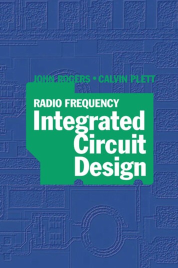
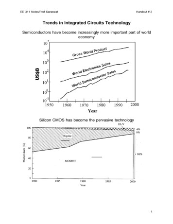
EE 311 Notes/Prof SaraswatHandout # 2Trends in Integrated Circuits TechnologySemiconductors have become increasingly more important part of worldeconomySilicon CMOS has become the pervasive technology1
Handout # 2Minimum lithographicfeature size (µm)Transistors or bits per chipEE 311 Notes/Prof SaraswatYearRef:YearTechnology node(DRAM half pitch)Minimum FeatureSizeDRAM Bits/ChipDRAM Chip Size(mm2 )MicroprocessorTransistors/chipMaximum WiringLevelsMinimum MaskCountMinimum SupplyVoltage (volts)A. I. Kingon et al., Nature 406, 1032 (2000).1997250 nm1999180 nm2003130 nm2006100 nm200970 nm201250 nm180 nm120 nm70 nm60 .8-2.51.5-1.81.2-1.50.9-1.20.6-0.90.5-0.6Future projections for silicon technology taken from the SIA ITRS 19992
EE 311 Notes/Prof SaraswatHandout # 2Ref. H. komiya IEEE ISSCC 1993Device structures are becoming increasingly more complexThe scaling trends for Intel microprocessors.3
EE 311 Notes/Prof SaraswatHandout # 2MOS Device ScalingLxoxScaled MOS TransistorXjN GN NaSDN N loPPWhy do we scale MOS transistors?1. Increase device packing density2.Improve frequency response (transit time) α1L3. Improve current drive (transconductance gm)gm ID VG VD constWµL nW µL n KoxVfor VD VD SAT , linear regionto x DKox(VG VT ) for VD VDSAT , saturation regionto xDecreasing the channel length and gate oxide thickness increases gm, i.e., the current driveof the transistor. Much of the scaling is therefore driven by decrease in L and tox. However ifonly these two parameters are scaled many problems are encountered, e.g., increasedelectric field.The most widely used scaling rule is to maintain the electric field in the device constantDevice/Circuit ParameterDimension :x o x, L, W, Xj,Substrate doping :NaSupply voltage :VSupply current :IGate Capacitance :W L/xo xGate delay :CV/IPower dissipation :C V2 / delayDelay power product :Constant Field Scaling Factor1/KK1/K1/K1/K1/K1/K21/K34
EE 311 Notes/Prof SaraswatHandout # 2Speed increases as a result of scaling10910the effect of bettermicroprocessorarchitectures8Number ofInstructions 107per Second486speed doubles each3-yr generation106105Pentium386802868080Intel Microprocessors40041041965197519851995So Does the Cost of a Factory10,0002x every 4 years1000cost of a modernwafer fab100( million)2x every 3 years1.47x every 2 years101196019701980199020005
EE 311 Notes/Prof SaraswatHandout # 2In reality constant field scaling has not been observed strictly. Since the transistorcurrent is proportional to the gate overdrive (VG-VT), high performance demands havedictated the use of higher supply voltage. However, higher supply voltage impliesincreased power dissipation (CV2f). In the recent past low power applications havebecome important and have required a scaling scenario with lower supply voltage.Ref: Davri, et al. Proc. IEEE, April 1995In general the device scaling methodology does not take into account many other chipperformance and reliability issues, e.g., interconnects, contacts, isolation, etc. Thesefactors are now becoming an obstacle in the evolution of integrated circuits.How far can we continue to scale?(Source: J. Plummer)6
EE 311 Notes/Prof SaraswatHandout # 2Effect of Reducing Channel Length: Drain Induced Barrier LoweringGateN sourceLDepletionregionL’N drainrjP-SiQB depletedby sourceQB depletedby drainIn devices with long channel lengths, the gate is completely responsible for depletingthe semiconductor (QB). In very short channel devices, part of the depletion i saccomplished by the drain and source bias. Since less gate voltage is required todeplete QB, the barrier for electron injection from source to drain decreasesPotential variation along the channel for MOS transistors with 2.5and 0.5 µm channel lengths. The 0.5 µm device shows DIBL effect.The reduction in the barrier is known as “drain induced barrier lowering (DIBL)”. DIBLresults in an increase in drain current at a given VG. Therefore VT as L . Similarly, as7
EE 311 Notes/Prof SaraswatHandout # 2VD , more QB is depleted by the drain bias, and hence ID and VT . This isAn approximate relation for threshold voltage due to DIBL is:VT VFB 2 φ F QBCox r 2 W 1 1 1 j rj L To minimize the effect of DIBL: Cox should be increased, i.e., decrease gate oxide thickness.This results in increased control of the gate. Decrease junction depth (rj )Scaling of gate oxide thickness and junction depth causes many other problems.Hot Carrier EffectsFor a reverse biased p-n junction discussion we remember that the maximum electricfield intensity is near the junction itself and it increases with the reverse bias.ξ max 2qN a (φ i VD )ε oxIn the case of MOS transistor the potential drop along the channel is not uniform withmost of it across the reverse biased drain-substrate junction. Therefore the electricfield intensity is also non-uniform with the maximum occurring near the drain junction.As the channel length is reduced the electric field intensity in the channel near thedrain increases more rapidly in comparison to the long channel case, even if VD i sscaled, as φi does not scale.8
EE 311 Notes/Prof SaraswatHandout # 2The free carriers passing through the high-field can gain sufficient energy to causeseveral hot-carrier effects. This can cause many serious problems for the deviceoperation.Hot carriers can have sufficient energy to overcome the oxide-Si barrier. They areinjected from channel to the gate oxide (process 1) and cause gate current to flow.Trapping of some of this charge can change VT permanently. Avalanching can takeplace producing electron-hole pairs (process 2). The holes produced by avalanchingdrift into the substrate and are collected by the substrate contact (process 3) causingIsub IR drop due to Isub(process 4) can cause substrate-source junction to beforward biased causing electrons to be injected from source into substrate (process5). Some of the injected electrons are collected by the reversed biased drain andcause a parasitic bipolar action (process 5).9
EE 311 Notes/Prof SaraswatHandout # 2Scaling of MOS Gate Dielectric(Ref: S. Asai, Microelectronics Engg., Sept. 1996)By the end of this decade the MOS gate dielectric thickness will be well below 10 Å.ID gm KthicknessHow far can we push MOS gate dielectric thickness?How will we grow such a thin layer uniformly?How long will such a thin dielectric live under electrical stress?Can we improve the endurance of the dielectric by changing its structure?Problems in scaling gate oxidePolysilicon gate electrodeDopantpenetrationLeakage currentgate oxideReliability due tocharge injectionDefects andnonuniformity of filmDielectric breakdownSi substrate10
EE 311 Notes/Prof SaraswatHandout # 2Gate Dielectric Degradation and BreakdownUnder high field electrons are injected in the SiO2 conduction band because ofreduction in barrier height and thickness. Some electrons gain excess energy in theconduction band of the oxide. At the anode they lose kinetic and potential energycausing physical damage leading to traps generation. Further trapping of electronsand holes causes dielectric degradation.eCathode(1) Electron injection(2) Energy released by hot electron(3) Bond breaking at the interface - trap generation(4) Hot hole generation by impact ionization and injection(5) Energy released by hot hole - trap generation(6) Hydrogen release - trap generation(1)(3)eOxide(5)h(2)(6)Anode(3) eHydrogen(4)hRef: Apte & Saraswat IEEE Trans. Electron Dev., Sept 1994We can improve the endurance of the dielectric by optimizing the process technologyand changing its structure. For example incorporating nitrogen or fluorine instead ofhydrogen strengthens the Si/SiO2 interface and increases the gate dielectric lifetimebecause Si-F and Si-N bonds are stronger than Si-H bonds.Poly-Si GateOxideN or FSi substrate11
EE 311 Notes/Prof SaraswatHandout # 2Problems caused by conduction in ultrathin gate oxideAs we decrease the gate dielectric thickness, the conduction through the dielectricfilm becomes appreciable. This may increase power dissipation and cause problemsfor circuit stability. Increased leakage due to direct tunneling through the gatedielectric may make dynamic and static circuits unstable.Thick OxideThin OxideFowler-Nordheim TunnelingDirect TunnelingOxideSiSi(Ref: From Y. Taur et al., Proc. IEEE, April 1997.)Gate Leakage Current Density Versus GateVoltage for Various Oxide Thicknesses12
EE 311 Notes/Prof SaraswatHandout # 2Current (µA/µm)1000Ion100.1Ioff0.001Source G. Bersuker, et al. SematechIgate0.000015070100130180Technology Generation (nm)Rather than scaling thickness of SiO2 perhaps we can scale the dielectric constant (K)to improve the performance. Alternatively for the same performance we can increasethe dielectric thickness by increasing its K.KID gm thicknesshigh K 20SiO2 K 440 Å20 ÅToday100 ÅSi 3N4 K 8Near futureLong termNear term and long term approaches for scaling the MOS gate dielectric.However, replacing SiO2 by another dielectric is a very difficult task as it isone of the best dielectrics and is one of the main reasons of the successof Si technology.13
EE 311 Notes/Prof SaraswatHandout # 2Scaling of Ohmic Contacts and d’Rddrain Device scaling dictates shallow junctions. How will we form such shallow junctions? How will we make low resistance contacts to them? What will be the impact of the resistance of the contacts and junctions?RcρCSource: Jasonn Woo, UCLAYearMin Feature SizeContact xj (nm)xj at Channel 5-3015-3020120.03µ10-2010-2014
EE 311 Notes/Prof SaraswatHandout # 2Specific contact resistivity 2φρc ρ co exp B qhεsm* N ohm cm 2where φB is the barrier height and N is the doping density in thesemiconductor.Problem in scaling: Contact resistance is a strong function of doping density at themetal/silicon interface Sheet resistance of a junction is a strong function of doping density inthe junction However, the maximum doping density is limited by solid solubility andit does not scale !15
EE 311 Notes/Prof SaraswatHandout # 2Solutions to Shallow Junction ProblemShallow extension implants to minimize (DIBL)Elevated source/ drain to minimize (DIBL)Silicidation to junction minimize resistance16
EE 311 Notes/Prof SaraswatHandout # 2Scaling of Device Isolation TechnologiesIsolation pitch as a function of minimum imum dimension [µm]0.81.0P. Fazan, Micron, IEDM-93LOCOS based isolation technologies have serious problems in loss of area due tobird’s beak.Semi-recessed LOCOSNitrideNitridePad oxideField oxideAfter field oxidationFully recessed LOCOSNitridePad oxideAfter field oxidationLarge stresses can build up in LOCOS based isolation technologies.F2F3F1F417
EE 311 Notes/Prof SaraswatHandout # 2Shallow trench isolationP-substrateN-wellDeep trench isolationTrench isolation can minimize area loss, however, large stresses can build up intrench structures resulting in bandgap reduction and eventually if the stress is toomuch it can cause crystal defects leading to increase in leakage and yield loss.10-11N P10-12Distance [µm]10-1310-14 05001000Compressive stress [MPa]1500The stress is a function of process temperatures as at higher temperatures SiO2 hasviscous flow which can relieve the stress. However, thermal budget demands lowtemperature processing.103900 C1021000 C1011100 C100110Active area pitch [ µm]10018
EE 311 Notes/Prof SaraswatHandout # 2Source: J. D. Meindl, , “Integration Limits on XXI Century Gigascale Integration”, IEEEInterconnect Technology Conf. Short Course, San Francisco, CA, May 31, 19981E8LocalSemiglobal 01001000Interconnect Length, l (gate pitches) Number of interconnects are increasing Most of the interconnects are very short but a few are very long19
EE 311 Notes/Prof SaraswatHandout # 2Impact of Scaling of Interconnections on Circuit Performance Chip area is increasing length of the longest wire is increasingCross sectional dimensions of the interconnects are decreasing resulting in anincrease in resistance and capacitanceIncreased R and C results in higher signal propagation delay500400CAPACITANCELine To GroundLine To LineTotal300200Capacitance (fF/mm)10000.0 0.5 1.0 1.5 2.0 2.5 3.0Space Width (µm) [ Line Width]Higher Packing Density Decreased Space BetweenInterconnects Higher RC-Delay20
EE 311 Notes/Prof SaraswatHandout # 2 Parasitic resistance and capacitance associated with interconnections andcontacts arenow begining to influence circuit performance and will be the primary factors in theevolutions of submicron ULSI technology. Lower resistivity metals and lower dielectric constant insulators will reduce the R and CDelay (ns)1.0Interconnect Delay0.1Typical Gate Delay0.016080100 120 140 160 180Technology Generation (nm).Copper 6Copper 5Copper 4Copper 3Copper 2Copper 1TungstenLocal InterconnectCurrent Cu technology (Courtesy of IBM)21
EE 311 Notes/Prof SaraswatHandout # 2globalsemigloballocalBy increasing the levels of wires interconnect problem can be minimized. Shorter(local) wires can be placed in thinner interconnects and longer (global) wires can bemade with larger cross section to minimize R and C.1413121110987654321Al & SiO2 (κ 4)Cu & SiO2 (κ 4)Al & low-κ (κ 2)Cu & lo w- κ ( κ 2)0.09 0.13 0.18 0.25 0.35 µm2007 2004 2001 1998 1995 YearTec hnology GenerationReduced resistivity and dielectric constant results in reduction in number of metal layersas more wires can by placed in lower levels of metal layers.22
EE 311 Notes/Prof SaraswatHandout # 2Problems in Scaling of InterconnectionsCu diffuses in most dielectrics readily and acts as a recombination centerin Si. Hence a barrier is generally needed to enclose Cu line to avoid itsdiffusion in the dielectric. Barriers are generally highly resistive.As λ decreases Resistivity increases as grain size decreases Resistivity increases as main conductor size decreases but not thesurrounding film sizeSurrounded InterconnectCuρavBarrierLayered InterconnectAlBarrierAlPure MetalInterconnectCuMinimum Feature Size (λ)23
EE 311 Notes/Prof SaraswatHandout # 24321035 50 70 100 1301801.210.80.60.40.20Thermal Conductivity[ W / mK ]Dielectric ConstantThermal Behavior Energy dissipated (CV2f) is increasing as performance improves Thermal conductivity of low-k insulators is poor Average chip temperature is rising30252015105054321035 50 70 100 130180Jmax [ MA / cm2 ]Power Density [ W / cm2 ]Technology Node [nm]Technology Node [nm]24
EE 311 Notes/Prof SaraswatHandout # 2ElectromigrationElectromigration due to electron wind induced diffusion of Al through grain boundariesSEM of hillock and voids formation due to electromigration in an Al(Cu,Si) lineMean time to failure due to electromigration is given byA E MTF m n exp a kT r J25
EE 311 Notes/Prof SaraswatHandout # 2Summary: Technology ProgressionMOS Transistor in 2010Gate oxide thickness 10 ÅChannel Length 500 ÅJunction depth 500 ÅSize of an atom 5 ÅA Circuit in 2010In integrated system 1 billion components 10 interconnect layers26
Trends in Integrated Circuits Technology Semiconductors have become increasingly more important part of world economy Silicon CMOS has become the pervasive technology. EE 31