Transcription
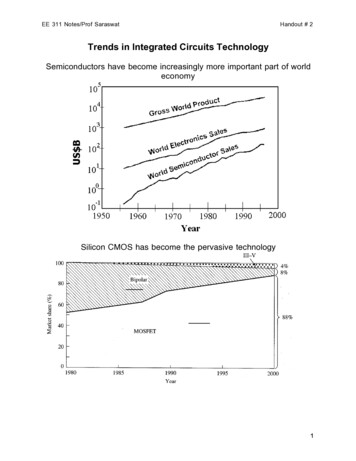
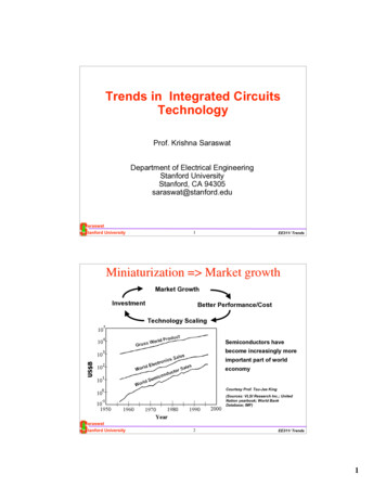
Trends in Integrated CircuitsTechnologyProf. Krishna SaraswatDepartment of Electrical EngineeringStanford UniversityStanford, CA 94305saraswat@stanford.eduaraswattanford University1EE311/ TrendsMiniaturization Market growthMarket GrowthInvestmentBetter Performance/CostTechnology ScalingSemiconductors havebecome increasingly moreimportant part of worldeconomyCourtesy Prof. Tsu-Jae King(Sources: VLSI Research Inc.; UnitedNation yearbook; World BankDatabase; IMF)araswattanford University2EE311/ Trends1
World IC Market by TechnologyRef: Chang and Sze, ULSI Technology, 1996Silicon CMOS has become the pervasive technologyaraswattanford University3EE311/ TrendsMoore’s LawTransistors Per 4K 16K105410i486 i486 64MPentium Pentium 4Pentium IIIPentium IIi386 8028680801K103256K16M2G 4G512M 1G256M128MItanium 40041028086IC Performance to Gordon Moore’s 0’95’00’05’10Source: Intelaraswattanford University4EE311/ Trends2
Feature Size 0 20102020Gate length is not true measure of transistor sizearaswattanford University5EE311/ TrendsExample: Microprocessor µIntel386 DXProcessorIntel486 DXProcessorPentium ProcessorPentium IIProcessoraraswattanford University6EE311/ Trends3
MOS Device ScalingConstant E Field ScalingAll device parameters are scaled bythe same factor α. Gate oxide thickness tox Channel length L Source/drain junction depth Xj Channel doping Supply voltage VD Why do we scale MOS transistors?1. Increase device packing density α22.Improve frequency response (speed) a3.Power/ckt: 1/α2, power density constant4.Improve current drive (transconductance gm)gm " ID"VG VD constWµnLW#µL n#araswatKoxVDfor VD VD SAT , linear regionto xKox(VG VT ) for VD VDSAT , saturation regionto xtanford University7EE311/ TrendsIntel’s Transistor Research down to 10nmElectronics is NanotechnologyDNA is 15 nm wide30nm65nm process2005 production20nm45nm process2007 productionSource: Intel15nm32nm process2009 production10nm22nm process2011 productionaraswattanford University8EE311/ Trends4
Speed increases as a result of scaling10010GateDelay 1(ps)0.1Limit0.010.0010.010.1LGATE (um)1Source: Mark Bohr, Intelaraswattanford University9EE311/ TrendsPhysical Limits in Scaling Si MOSFETGate stack Tunneling current Increased Ioff Gate depletion Increased EOTSource/Drain Contact resistance Doping level, abruptnessHigh E-Field Mobility degradation ReliabilityGateSourceDrainSubstrateteChannel Surface scattering - the “universal mobility” tyrannyDIBL drain to source leakageSubthreshold slope limited to 60mV/decade (kT/q) Increased IoffVG - VT decrease reduced IONNet result: Bulk-Si CMOS device performance increase commensurate withsize scaling is unlikely beyond the 70 nm nodearaswattanford University10EE311/ Trends5
MOSFET Scaling Limit: LeakageTotal Leakage TrendGate LeakageS/D LeakageTotal Power TrendsSource: Marcyk, IntelAbility to control Ioff will limit gate-length scaling–––To suppress D/S leakage, need to use:–Higher body doping to reduce DIBL lower mobility, higher junction capacitance, increased junction leakage– Thinner gate dielectric to improve gate control higher gate leakage– Ultra-shallow S/D junctions to reduce DIBL higher Rseriesaraswat11tanford UniversityEE311/ TrendsMOSFET Scaling Problem: Saturation of IDsatRelaxed OFF current LimitConstantOFF current Limit510I Dsat (A/m)4 (drive current)800600NMOS4002000.250.1 0.2PMOS0.3 0.4 0.60.81.01.20.80.4Channel Length (µm)log IdSource: Intel01990Low Vt1995120052000 Data from IBM, TI, Intel, AMD, Motorola andLucentHigh VtIOFF,low VtSupply Voltage (V) Thermionic emission over barrierQM tunneling through barrierBand-to-band tunneling from body to drainDrive Current (mA/µm) Lo et al.,IEEE EDL, May 1997. Low OFF current desirableIOFF,high Vtaraswat0tanford UniversityVgChanghoon Choi, PhD Thesis, Stanford Univ., 200212EE311/ Trends6
PhononulombicEffects of Scaling Bulk MOSFET on MobilityCoµSurfaceRoughnessEeff1111 µ eff µC µ ph µ srE effS. Takagi et al., IEEE TED, 41 (1994) 2357.q (N dep # NChannel )"SiNdep depletion charge densityNChannel charge induced in the channelIncreases in substrate doping Ndep Gate oxide thickness decrease NChannel ! Eeff increases with scaling µ Reduced gate oxide thickness increases remote charge scattering µ High k dielectrics have higher coulombic scattering due to surface statesand phonon scattering µ araswattanford University13EE311/ TrendsNew Structures and Materials forNanoscale MOSFETs5342Top GateGSCD1High µchannelSiBULKSourceSiSiO2DrainBottom GateHigh-KDouble gateSOI1. Electrostatics - Double Gate- Retain gate control over channel- Minimize OFF-state drain-source leakage2. Transport - High Mobility Channel- High mobility/injection velocity- High drive current for low intrinsic delay3. Parasitics - Schottky S/D- Reduced extrinsic resistance4. Gate leakage - High-K dielectrics- Reduced power consumption5. Gate depletion - Metal gatearaswattanford University14EE311/ Trends7
Combining New Device Structures withNew MaterialsWe will be here withthese innovationsWe arehere today With better injection and transport we may be able toimprove MOSFET ION With better electrostatics we may be able to minimize Ioffaraswattanford University15EE311/ TrendsNanotechnology Eras0.110065 nmGeneration45 nm32 nmLGATE22 nm16 nm11 nmmicron 0.018 yDifferentSource: Mark Bohr, Intelaraswattanford University10 nm16EE311/ Trends8
Scaling of MOS Gate DielectricKID ! gm !thickness(Ref: S. Asai,Microelectronics Engg., Sept. 1996)Gate SiO2 thickness is approaching 10 Å to improve device performance How far can we push MOS gate dielectric thickness? How will we grow such a thin layer uniformly? How long will such a thin dielectric live under electrical stress? How can we improve the endurance of the dielectric?araswattanford University17EE311/ TrendsProblems in Scaling of Gate OxidePolysilicon gate electrodeDopantpenetrationLeakage currentgate oxideReliability due tocharge injectionDefects andnonuniformity of filmDielectric breakdownSi substrate Below 20 Å problems with SiO2– Gate leakage circuit instability, power dissipation– Degradation and breakdown– Dopant penetration through gate oxide– Defectsaraswattanford University18EE311/ Trends9
Dielectric Degradation Degradation during device operation due to high E field causing current injection Degradation during fabrication due to charging in plasma processingEoxeEcathodeN(E)oxideAnodeWhat are the mechanisms for damage and breakdown?How can we engineer the gate dielectric to minimize the damage?araswattanford University19EE311/ TrendsGate Oxide Scaling Issues: LeakageCurrent (µA/µm)1000Ion100.1Ioff0.001Source G. Bersuker, et al. SematechIgate0.000015070100130180Technology Generation (nm) Ion is not increasing with scaling Igate , power dissipation Circuit instabilityaraswattanford University20EE311/ Trends10
High-k MOS Gate DielectricsIchannel charge x source injection velocity (gate oxide cap x gate overdrive) vinj Cox (VGS - VT) Esource µinjHistorically Cox has been increased by decreasing gate oxidethickness. It can also be increased by using a higher K dielectricID " Cox "Today20!Å SiO2 K 4KthicknessLong termNear future100 Å high K40 ÅK 20Si3N4 K 8SiHigher thickness - reduced gate leakagearaswattanford University21EE311/ TrendsCapacitance and Leakage for High-k GateDielectric Films Grown Using ALCVDGate Leakage (A/cm2)m1c/V 0Gate Current@ VFB 1V (A/cm2)VSiO22.5 nmALCVDZrO24 nm-1000.050.11/C'ox0.150.22(µm /fF)Equivalent SiO2 Thickness (nm)Perkins, Saraswat and McIntyre,Stanford Univ.Univ. 2002Chui, Kim, Saraswat and McIntyre,Stanford Univ.Univ. 2004araswattanford University22EE311/ Trends11
Subthreshold BehaviorOFFVDD - VTID(log scale)ONVTFermi DiracdistributionVDDS ILEAK orIOFFIONsource!VG! (ln I D ) Diffusion of carriers over thebarriers to the channel. Fermi-dirac distribution ofcarriers: e-E/kT Gate reduces the barrier tocurrent flow.VGQI " eq# s / kT!s f (VG ) 1V" GI D " QI " eq VG / # kTWherearaswat" 1 1#2CoxdraineVG60 mV/decadeq s N a %p tanford University23EE311/ TrendsEffect of Reducing Channel Length In devices with long channel lengths, the gate is completely responsible fordepleting the semiconductor (QB). In very short channel devices, part of thedepletion is accomplished by the drain and source bias Since less gate voltage is required to deplete QB, VT as L . Similarly, as VD , more QB is depleted by the drain bias, and hence VT . These effects areparticularly pronounced in lightly doped substrates.VTpoly gaten n p-substratedepleted bygate chargejunctiondepletionregionpoly gaten Drawn Channel Length, LVTn p-substrateSupply Voltage, VDaraswattanford University24EE311/ Trends12
Drain-Induced Barrier Lowering (DIBL) Exacerbates subthreshold leakage in short-channel devices Soft punchthrough induced by drain-to-substrate depletion region VT as VD [drain-induced short channel effects (SCE)] VD drain-to-substrate depletion region grows with more reverse bias Lateral electric fields in drain-induced depletion region lowers source-tochannel barrier, allowing more carriers to diffuse from source to channelVDDpoly gatepoly gaten n n p-wellCBn p-wellsourcedrainreduction of electron barrierheight in conduction band (CB)at edge of sourceVDDaraswattanford University25EE311/ TrendsWhy do we need to scale junction depth?GateN sourceLDepletionregionL!N drainrjP-SiQB depletedby sourceQB depletedby drainQ * 2 " W ' rj VT VFB ! 2 " # F ! B " ,1 ! & 1 ! 1) " /Cox %rj( L. Roll-off in threshold voltage as the channel length is reduced VT roll-off is reduced as junction depth(rj) is decreased Sheet resistance increases as junction depth is reducedL. Yau, Solid-State Electronics, vol. 17, pp. 1059, 1974araswattanford University26EE311/ Trends13
Series Resistance (ohms)Source/Drain Resistancey 0SiO2GateMetalRcRext RovRdpNov(y)xNext(x)140120 NMOS100Scaled by ITRS Roadmap80Rext60RdpRc40200Rov30 nm 50 nm 70 nm 100 nmPhysical Gate LengthSource: Jasonn Woo, UCLAProblem in junction scaling: Sheet resistance of a junction is a strong function of doping density Maximum doping density is limited by solid solubility and it does not scale Silicidation can minimize the impact of junction sheet resistance (Rs,Rd) Contact resistance Rc is one of the dominant components for future technologyaraswattanford University27EE311/ TrendsContact ResistanceSpecific contact resistivity 2"!c ! co exp && B% qh#sm* ')N )(ohm * cm 2Doping densityPROBLEMS Contact resistance is a strong function ofdoping density at the metal/silicon interface Solid sulubility of dopants does not scale !(Ref: S. Swirhun, PhD Thesis, Stanford Univ. 1987)araswattanford University28EE311/ Trends14
Solutions to Shallow JunctionResistance ProblemExtension implantsElevated source/ drainSchottky Source/DrainSilicidationaraswattanford University29EE311/ TrendsProblems with Poly-Si Gate.This occurs because of high E - field due to a combination of highersupply voltage and thinner gate oxide.Poly-Si gateGate e Effect of depletion is to increase effective t ox and thus reduce Cox A reduced Cox implies reduction in gm and thus ID(on) Ionized impurities in the gate electrode cause “remote charge scattering” Reduced mobilityaraswatNeed metal gate electrode with proper workfunctiontanford University30EE311/ Trends15
Evolution of MOSFET StructuresUltra-Thin Body Single Gate SOIBULKGateSourceSOISiDrainSiO2TBOXSilicon SubstrateAdvantages of Ultra-Thin Body SOI Depleted channel no conduction pathis far from the gate Short channel effects controlled bygeometry Steeper subthreshold slope Lower or no channel doping Higher mobility Reduced dopant fluctuationUltra-Thin Body DoubleGate SOISourceToxGate 1VgSOIDrainSiGate 2Ref: Philip Wong, IEDM Short Course, 1999araswattanford University31EE311/ TrendsNon Planar MOSFETsVertical FETTri Gate FETDouble Gate , AT&TUC BerkeleyDrainIntelaraswattanford University32EE311/ Trends16
Transport: Effects of Biaxial Tensile Strain on Si Energy BandsHoyt, 2002Strained Si grown on Relaxed Si1-xGex[001]biaxial tension Δ2Conduction BandAdditional splitting: Band repopulationBulk Si[010]EcStrained SiΔ4Δ6Δ Es 67 meV/10% GeΔ2Δ4[100]- reduced intervalleyscattering- smaller in-plane effectivetransport massµ q!m*cmtmtBulk Si EValence BandΓHH/LH degeneracy lifted at Γmt mlStrained Si Ekin-planeΔ Es 40meV/10% GeHH- reduced interband scattering- smaller in-plane transportmass due to band deformationSingle ellipsoidmlout-ofplanekLHSpin-Orbitaraswattanford University33EE311/ TrendsMobility Enhancements in Strained-Si MOSFETsoitargate oxidePMOSLTOspacerStrained Sitnemecna 2.0hn 1.8eMobility Enhancement Factorn polyNMOSRelaxed Si1-xGex n n Si1-xGex Graded layerSi SubstrateVDS 10 mV300 K1.6yt 1.4ili 1.2bo 1.0M0.800.0Measured, J. Welser, et al.,IEDM 1994.Calculated for strained SiMOS inversion layerS. Takagi, et al., J. Appl. Phys. 80, 1996.0.100.200.300.40Substrate Ge fraction, xGibbons Group, StanfordIntelaraswattanford University34EE311/ Trends17
Nanowire and Nanotube FETsGe NW GrowthALD HfO2 Coated of Ge NW FETGeContainingVapormetalChanneldielectric 20nmsemiconductorAuNanoparticle 10nmGeNanowiredraingatesourceCarbob Nanotube MOSFETCarbob Nanotube GrowthGateDHfO2S10 nm SiO2CnHmFep SiCnHmCatalyst SupportKey Challenge: Controlled growtharaswattanford University35EE311/ TrendsSeemingly Useful DevicesLimited Current DriveCryogenic operationLimited Fan-OutCritical dimension controlChallenging fabricationand process integrationB 2 nmSpintronicsNeed high spin injectionand long spin coherence timearaswattanford UniversityLimited thermal stabilityNew architectures needed36CarbonNanotubesControlled growthEE311/ Trends18
In general this device scaling methodologydoes not take into account many other chipperformance and reliability issues, e.g.,interconnects, contacts, isolation, etc. These factors are now becoming an obstaclein the evolution of integrated circuits.araswattanford University37EE311/ TrendsActive Area pitch (µm)Device Isolation pitch as a function ofminimum dimension2.52.064M1.51G1.00.50.0araswat16MP. Fazan, Micron, IEDM-930.00.20.40.6Minimum dimension [µm]0.81.0With decreasing feature size the requirement onallowed isolation area becomes stringent.tanford University38EE311/ Trends19
Scaling of Device IsolationSemi-recessed LOCOSNitrideNitridePad oxideField oxideAfter field oxidationFully recessed LOCOSLOCOSbased isolation technologies have serious problemsNitride of area due to bird’s beak.in lossPad oxideShallow trench isolationAfter field oxidationP-substrateN-wellDeep trench isolationTrench isolation can minimize area lossaraswattanford University39EE311/ TrendsScaling of interconnectionsNew (scaled)Old Bigger chip longer interconnects Scaling to smaller dimensions reduced cross section Larger R, L and Caraswattanford University40EE311/ Trends20
Interconnect Delay Is Increasing Chip size is continuallyincreasing due toincreasing complexity– Increase in R, L and C Device performance isimproving but interconnectdelay is increasingDelay Time (ns)scaling101Longest Interconnect Delay10010-1Typical Gate Delay Need better materials10-2– Metal with lower resistivity– Dielectrics with lower K– Other solutions, e.g., 3D,optical interconnectsaraswattanford University6080100120 140 160 180Technology Node (nm)41EE311/ TrendsAdvances in Backend Technology1970’s1980’s1990’sPoly-Si gateAluminumAluminum alloysSilicide contactsPolycide gatesLocal planarizationLayerd aluminum/titaniumSalicidesCVD tungsten plugsShallow trench isolationGlobal planarizationaraswattanford University42EE311/ Trends21
Current Interconnect TechnologiesCopper 6Copper 5Copper 4Copper 3Copper 2Copper 1TungstenLocal InterconnectCurrent Cu technologyCurrent Al technology(Courtesy of Motorola)(Courtesy of IBM)araswattanford University43EE311/ TrendsWhy Cu and Low-k Dielectrics?1413121110987654321Al & SiO2 (! 4)Cu & SiO2 (! 4)globalsemiglobalAl & low-! (! 2)localCu & lo w- ! ( ! 2)0.09 0.13 0.18 0.25 0.35 µm2007 2004 2001 1998 1995 YearTec hnology GenerationSource: Y.NishiReduced resistivity and dielectric constant results in reduction in number ofmetal layers as more wires can by placed in lower levels of metal layers.araswattanford University44EE311/ Trends22
Cu Resistivity: Effect of Line Width Scaling Effect of Cu diffusion Barrier Barriers have higher resistivity Barriers can’t be scaled below a minimum thickness Effect of Electron Scattering Reduced mobility as dimensions decrease Effect of Higher Frequencies Carriers confined to outer skin increasing resistivityProblem is worse than anticipated in the ITRS 1999 roadmaparaswattanford University45EE311/ TrendsProblems in Scaling of InterconnectionsSurrounded InterconnectAS λ DECREASESCuBarrier Resistivity increases asgrain size decreasesρavLayered InterconnectAl Resistivity increases asmain conductor sizeBarrierAldecreases but not thePure MetalInterconnectsurroundingbarrier sizeCuMinimum Feature Size (λ)araswattanford University46EE311/ Trends23
3-D Integration: Motivation2D Area AVery Long Wire3DA/2A/2Number of Interconnects(Log-Log Plot)2-D IC3-D ICWire-lengtharaswattanford University3-D System2-D SystemShorter Wire Integration of heterogeneous technologiespossible, e.g., memory & logic, optical I/O Reduce Chip footprint Replace long horizontal wires by shortvertical wires Interconnect length and therefore R, L, C – Power reduction– Delay reduction47EE311/ TrendsNo. Transistors/chip //Perf/FunctionalitySource: D. Radack, DARPA3D batchRepeaters oroptical I/O devicesGaten /p n /p M4M3M2M1Gaten /p n /p 3-D PackagingMemoryorAnalogM’1LogicGaten /p 2-D Batch12-15 yearsTimeT2M’2n /p T1No. Transistors per cm3 in system3-D Motivation: Integration DensityEnd-of-Moore’sLaw!The Best Integrators of Electronic Devices Will Own theHeart of Every System – We have 15 Years to Figure it outaraswattanford University48EE311/ Trends24
Can Optical Interconnects help?On-ChipOpticalInterconnects40Tb/sOptical I/O1024x OC-768100Tb/sOn-ChipBisection BWPMM64 Tiles64b Processor 4MB DRAMChip-to-chip Optical InterconnectsCan potentially address many problems ofCu/low-k wires On-Chip Links Clocking and Synchronization High Bandwidth off-chip LinksReduce power Reduce delay Reduce jitter and skewaraswattanford University 49EE311/ TrendsResult: scaling of power componentsChandra, Kapur and Saraswat,IEEE IITC, June 2002ITRS projections for totalpower dissipation on chip Dynamic Power: CV2f Leakage power: devices Short circuit power during switching Static power, e.g., analog components (sense amps etc.)Power increasingly becoming the performance bottleneck for high-endmicroprocessorsaraswattanford University50EE311/ Trends25
21035 50 70 100 130180Power Density [ W / cm2 ]31.210.80.60.40.203025201510505Jmax [ MA / cm2 ]4Thermal Conductivity [W / mK ]Dielectric ConstantThermal Behavior in ICs4321035 50 70 100 130180Technology Node [nm]Technology Node [nm] Thermal conductivity of low-k insulators is poor Thermal impedance increases Energy dissipated (CV2f) is increasing as performance improves Average chip temperature is risingSource: ITRSaraswattanford University51EE311/ TrendsThe problems Caused by Increased PowerRELIABILITYElectromigration induced hillocks and voidsVoidHillockMetalDielectricMetalMean time to failure 100A will flow on these wiresMTF "E %Aexp a 'n# kT &r Jm10 C , MTF 50%PERFORMANCE!As T R , RC delay 10 C , Speed 5%araswattanford University52EE311/ Trends26
Conclusion: Technology ProgressionBulk CMOSStrained SiSi(tensile)Cu interconnectSi0.8Ge0.2Si1-xGexFeature Size3D ICsFD SOI CMOSWafer bondingCrystallizationNanowiresOptical interconnectSiLow-k ILDDouble-Gate CMOSGateMetal gateHigh k gate dielectricSourceDrainDetectors, lasers,modulators, waveguidesGe/Si HeterostrctureSingle etransistorGe on Si hetroepitaxyGe on InsulatorMolecular deviceNanowireBNanotube Spin deviceTime2 nmaraswattanford University53EE311/ TrendsSummaryMOS Transistor in 2010A Circuit in 2010A Factory in 2010Gate oxide thickness 1nmApproaching 10 billionChannel Length 2nm1010 componentsJunction depth 1-2nmIntegrated digital, analog, sensorsSize of an atom 5 ÅQuestions we are trying to answer How can we continue the Moore’s law What will be new materials, devices, circuits, sensors,equipment, simulators, etc. How will we design them?araswat How will we manufacture them?tanford University54EE311/ Trends27
Trends in Integrated Circuits Technology ta nfo rdU ivesy 2 EE311/ Trends araswat Courtesy Prof. Tsu-Jae King (Sources: VLSI Research Inc.; United Nation yearbook; World Bank Database; IMF) Miniaturization Market growth Technology Scaling Investment Market Growth Better Performance/Cost S