Transcription
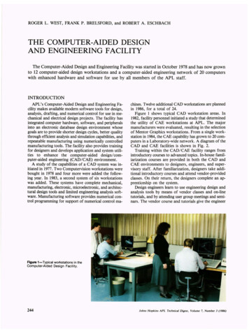
ROGER L. WEST, FRANK P. BRELSFORD, and ROBERT A. ESCHBACHTHE COMPUTER-AIDED DESIGNAND ENGINEERING FACILITYThe Computer-Aided Design and Engineering Facility was started in October 1978 and has now grownto 12 computer-aided design workstations and a computer-aided engineering network of 20 computerswith enhanced hardware and software for use by all members of the APL staff.INTRODUCTIONAPL's Computer-Aided Design and Engineering Facility makes available modem software tools for design,analysis, drafting, and numerical control for use in mechanical and electrical design projects. The facility hasintegrated computer hardware, software, and peripheralsinto an electronic database design environment whosegoals are to provide shorter design cycles, better qualitythrough efficient analysis and simulation capabilities, andrepeatable manufacturing using numerically controlledmanufacturing tools. The facility also provides trainingfor designers and develops application and system utilities to enhance the computer-aided design/comp\lter-aided engineering (CADI CAE) environment.A study of the capabilities of a CAD system was initiated in 1977. Two Computervision workstations werebought in 1978 and four more were added the following year. In 1983, a second system of six workstationswas added. These systems have complete mechanical,manufacturing, electronic, microelectronic, and architectural design tools and limited engineering analysis software. Manufacturing software provides numerical control programming for support of numerical control ma-chines. Twelve additional CAD workstations are plannedin 1986, for a total of 24.Figure 1 shows typical CAD workstation areas. In1982, facility personnel initiated a study that determinedthe utility of CAE workstations at APL. The majormanufacturers were evaluated, resulting in the selectionof Mentor Graphics workstations. From a single workstation in 1984, the CAE capability has grown to 20 computers in a Laboratory-wide network. A diagram of theCAD and CAE facilities is shown in Fig. 2.Training within the CAD/CAE facility ranges fromintroductory courses to advanced topics. In-house familiarization courses are provided in both the CAD andCAE environments to designers, engineers, and supervisory staff. After familiarization, designers take additional introductory courses and attend vendor-providedclasses. On their return, the designers complete an apprenticeship on the system.Design engineers learn to use engineering design andanalysis tools by means of vendor classes and on-linetutorials, and by attending user group meetings and seminars. The vendor course and tutorials give the engineerFigure 1-Typical workstations in theComputer-Aided Design Facility.244Johns Hopkins APL Technical Digest, Volume 7, Number J (1986)
Departments Technical ServicesSubmarine Tech ute(centralprocessor)16 AEnetworkITape drivePunchReaderPrinterFigure 2-Diagram of the Computer-Aided Design and Engineering Facility.the necessary knowledge to begin using the tools productively. On-site user meetings and seminars, which provide for exchanges of practical information among theparticipants on the network, discuss fIxes, work-arounds,general design techniques, and specifIc design problems.Systems operation and programming staffs are available for development of software utilities, hardware interfacing, and general consulting. When a user has aproblem, the facility's staff works with him to solve it.The work flow of a design project starts with a concept developed by an engineer that is turned into a complete design using an integrated collection of softwaretools. The design is then transformed into a manufacturing data package that is used to develop instructionsfor numerically controlled manufacturing machines.Both mechanical and electrical designs follow this basicpath; however, the design flow and software tools required are quite different.A mechanical design begins with a concept of the confIguration and the functional requirements. Engineeringdesigners develop the layout and analyze critical itemslike flexure, vibration response, and mass properties bymeans of fInite-element and stress-analysis codes. Using this information, drafters make detailed drawings todescribe the various parts for manufacturing. The detailed drawings are turned into machine-tool controlcommands by a numerical control programmer using information directly from the part's design database.Electrical CAE software enables the engineer to develop an electrical schematic, using circuit simulation,timing, and fault analysis tools. CAD software then permits the layout designer to transform the design database into parts lists, circuit board artwork, and controlcommands for automatic fabrication tools. Part placement on the circuit boards is also specifIed. Outputs fromthese systems are also available for custom very largescale integrated (VLSI) circuitry and gate-array fabricaJohns Hopkins APL Technical Digest. Volume 7. Number 3 (1986)tion. (A detailed description of mechanical and electrical CAD design is given in the article by Schachtner andAhlbrand.)THE COMPUTER-AIDEDENGINEERING FACILITYAPL's CAE network uses the Mentor Graphics software tools for electrical design. Mentor software is executed on Apollo computers that provide a wide rangeof hardware capabilities at each workstation. The Apollocomputer workstation nodes are connected in a highspeed token ring network to allow the sharing of hardware, software, and data resources among the workstations. Apollo computer systems support three majoroperating systems: AEGIS, developed by Apollo Computer, and two versions of UNIX. General-purpose language support includes Pascal, Fortran, C, and LISP.Utilities are available for graphics, communications,peripheral interface, and software development.The hardware and software for each CAE workstation have been selected to meet APL's engineering needs.Approximately 200 companies are offering CAE software tools for the Apollo system. Architectural, chemical, civil, electrical, mechanical, power systems, softwaredesign, and structural engineering disciplines are addressed. Additional APL interest and usage include dataanalysis, artifIcial intelligence, software development,and the study of distributed computing concepts.Currently, the central CAE facility contains two workstations, a compute node and a server node. Sixteen other workstations are distributed throughout APL. Planscall for a network of approximately 40 CAE workstations by 1989. Sixteen of the current workstations support Mentor Graphics software tools (Fig. 3), and fourworkstations execute P ATRAN for pre- and post-processing of CAD models for finite-element analysis.245
West, Brelsford, Eschbach -Computer-Aided Design and Engineering FacilityFigure 3-CAE workstation located in the facility. The screenshows Mentor Graphics electrical design software.The Mentor software tools support electronic designfunctions for all phases of digital design. These coverschematic capture, logic and fault simulation, timing verification, gate-array cell placement and route, and custom VLSI design. A standard user interface across thedesign tools enables the designer to transfer experiencewith one software tool to the others.Three recent projects-a digital gate-array design, awire-wrapped circuit design, and a finite-element analysis of solder joints-display APL's use of CAE designtools. The fIrst used a Department of Defense very-highspeed integrated circuit gate-array description from TexasInstruments to develop an integrated circuit for interfacing with other very-high-speed integrated circuit components (see the article by Charles et al.). The seconddeveloped a digital circuit containing approximately 700integrated-circuit components mounted on six circuitboards. Finally, the PATRAN software tool modeledsolder joints of leadless ceramic chip carriers in the presence of thermomechanical stress (see the article by Clatterbaugh and Charles).The three projects represent uses of CAE workstationsthat would have been diffIcult or impossible without thedesign tools. The gate-array design requires communication of the upper metal-interconnect layers of the gatearray to Texas Instruments for its manufacturing process.The second example displayed a more complex useof the Laboratory's CAD environment. After the digital design is input and simulated on a Mentor workstation, it is transferred to the CAD system for physicallayout and documentation. Utilities extract a netlist fromthe CAE design and translate between the CAD andCAE formats. On the CAD system, a layout designerperforms the automatic placement and routing functionsthat position the components and assign the digital gatesto physical packages. Component location and pin numbers are back-annotated to the Mentor design for accurate circuit documentation. The CAD system provides246Figure 4-The Hardware Verification System being used to veri·fy a gate array.drawings of the populated circuit boards, a parts list,and control data for a semiautomatic wire-wrap machine. Finished wire-wrap boards can be electrically connected to the Mentor Hardware VerifIcation System (seeFig. 4). This hardware converts simulation test vectorsinto digital input signals to the boards and records theoutput signals. Comparison of the simulation and circuit outputs provides verification of the manufacturingprocess.COMPUTER-AIDED DESIGN FACILITYOutputs from the CAE workstation or hand drawingsprovide inputs to the CAD system. The CAE workstation input permits the engineer to transfer data directlyto the designer's CAD tool instead of having it duplicated on the CAD system. This capability provides afaster and more accurate method of passing along thedesign information.Mechanical DesignThe mechanical design software is used to producetwo- and three-dimensional design layouts, assemblies,detail drawings, and numerical control outputs. The system's three-dimensional capabilities in the software's"model mode" are used primarily for conceptual designand interference checks on proposed hardware. Programs such as the Hopkins Ultraviolet Telescope, DualDoppler Beacon, and Standard Rampart have made useof this capability. Figure 5 shows a drawing of the telescope; the article by Schachtner and Ahlbrand providesfurther examples. The models are wire frame drawings;a color workstation is used to discriminate parts. Thedrawings can be quickly rotated to any angle with conJohns Hopkins APL Technical Digest, Volume 7, Number 3 (/986)
West, Brelsford, Eschbach - Computer-Aided Design and Engineering FacilityoIIFigure 5-Plot of the sensor assembly from the Hopkins Ultraviolet Telescope, contained in the CAD model. Note how color isused to separate different components.trolled perspective for better visualization, interferencechecking, or modification.Individual two-dimensional detail drawings are derivedfrom the model. Detailed fabrication drawings are madeby semiautomatically adding dimensions and text to theexisting part drawing. Drawing formats, standard notes,and other repetitive items are called up from the system's library and quickly added. The system has hardcopy output to electrostatic Versatec plotters on paper,vellum, or mylar fllm. Color plots, with up to eightcolors, can be made with a pen plotter.When computer-aided manufacturing is applicable forparts fabrication, the data used to control the relatedmachines are produced on the CAD system. The numerical control programmer uses the geometry portion ofthe design database to defme a "tool path." After verifiJohns Hopkins APL Technical Digest, Volume 7, Number 3 (/986)cation, the tool path is transferred to punched paper tapefor use by the machine tool.Engineering information for mechanical parts is alsogenerated by the CAD system. Mass properties including center of gravity and moments of inertia are extracteddirectly from the model database. Although not as capable as the CAE software, a finite-element model forstress analysis of the part can be constructed. The finiteelement model is transferred to the NAS 9160 computeranalysis, after which the results are transferred back tothe system for dynamic display of the distorted model.Electrical DesignThe CAD system provides a variety of tools for usein printed circuit!electrical schematic design. The printedcircuit!electrical schematic application package provides247
West, Brelsford, Eschbach - Computer-Aided Design and Engineering Facilitydocumentation for a printed circuit board equivalent tothat obtained by manual drafting methods. Schematics,parts lists, layouts, artwork, assembly drawings, and detail drawings are prepared on the system using approvedAPL drawing formats.Schematic diagram are prepared by inserting libraryfigures and then copying, moving, and connecting themas required. Text is then added to complete the drawing. The fIle structure allows access to multisheet schematics as if they were a single database. The operatorcan place parts in approximate positions, use nonorthogonal lines to interconnect them, and get a neat finaldrawing. Other commands check the database, createformatted listings of user-selected parameters, extractnetwork data from schematics, and create a netlist. Partslists, bills of material, and post-process data for use withother systems are also available.Printed circuit board layout is performed using theprinted circuit!electrical schematic package. Automaticpart placement speeds the process of designing printedcircuit boards. With this program, the designer directscomponent placement. He may also pre-place components, gates, or pins that will not be changed. The computer assigns gates to components and places the remaining components on the board.Automatic routing of printed wiring is also performedby the printed circuit!electrical schematic applicationsoftware. Starting with a placed printed circuit board,the program automatically routes the printed wiring. Thisestablishes interconnections between pins having thesaine signal name while avoiding user-defmed obstaclessuch as tooling or mounting holes, user-described keepout areas, and pads. The router may be stopped formanual editing and then restarted to complete the process. A well-placed board results in an initial completion rate of at least 95 percent completed routing. Afterthe operator interactively finishes the design, a comparison of the original schematic netlist with the circuitboard database is performed. A user-defined rule fIleperforms geometric checks on the routed circuit board.A completed board is shown Fig. 6.During the design process, data needed to create drawings, numerical control tapes, and magnetic tapes forphotoplotting are stored in the design database (see thearticle by Strider and Wagner). Necessary manufacturing drawings are created by selecting the database in-248Figure 6-A designer modifying routed interconnects on anNROSS circuit board. Only two of the interconnect layers areshown.formation and adding required dimensional data andtext. Data used for drilling and routing the printed circuit board are extracted from the database and automatically coded for the numerically controlled manufacturing tools.THE FUTURE OF CAD AT APLThe engineering, design, and fabrication communityat APL is rapidly expanding its use of computers to increase productivity, enhance quality, and consolidate information transfer. The CAD and CAE facilities capabilities are being expanded and refmed to take advantageof new developments including the use of personal computers. Information flows from the conceptual designto fabrication without a manual or paper interface. Selection of hardware and software and the design of workflows will continually enhance this ideal.ACKNOWLEDGMENTS-We wish to thank the following people for theirsignificant contributions to the selection and development of the CAD system:R. E. Hicks for hybrid and microelectronics development, R. G. Heidelbach forsystem implementation and mechanical development, W. J . Roemer for mechanical development, and J. P. Schmidt III for development of numerical controlprogramming. We also wish to acknowledge the help of the CAD system manager, L. M. Schweitzer, and the following full-time operators and associates: M .Puritz, J. F. Rider, J. E. Hughes, K. W. Padgett, C. E. Shade, D. Gentilucci,and S. L. Kohout.Johns Hopkins APL Technical Digest, Volume 7, Number 3 (/986)
West, Brelsford, Eschbach - Computer-Aided Design and Engineering FacilityTHE AUTHORSROGER L. WEST (right) was born in Providence, R.I., in 1948.He received his Sc.B. in physics from Brown University (1970), amaster's degree from Iowa State University (1972), and a Ph.D. fromthe University of Notre Dame (1977) in low-energy nuclear physics. After studying low-energy polarized scattering at Ohio State University, he joined APL in 1977. As a member of the Strategic SystemsDepartment, he characterized and modeled inertial navigation systems . Dr. West is now supervisor of the Computer-Aided DesignGroup in the Technical Services Department and is an instructorfor VLSI design in the G.W.C. Whiting School of Engineering PartTime Engineering Program at APL.FRANK P. BRELSFORD (center) was born in Schenectady in1942. He received his B.A. in mathematics (1969) and his M.S. inphysics (1971) from Miami (Ohio) University. He joined APL in1973 as a member of the Strategic Systems Department, where heconducted weapon system evaluations. Mr. Brelsford received a second master's degree in electrical engineering from The Johns Hopkins University Evening College in 1977. He is now the computeraided engineering network manager for APL's Technical ServicesDepartment. Mr. Brelsford is an instructor for microprocessor software in the G.W.C . Whiting School of Engineering Part-Time Engineering Program at APL.Johns Hopkins APL Technical Digest, Volume 7, Number 3 (1986)ROBERT A. ESCHBACH (left) was born in Chicago in 1924.He joined APL in 1960 as a member of the Space Department, wherehe participated in electronic packaging design activities . He was asection supervisor in 1966 in charge of electronic packaging. Mr.Eschbach now supervises microelectronic packaging design in theTechnical Services Department.249
The Computer-Aided Design and Engineering Facility was started in October 1978 and has now grown to 12 computer-aided design workstations and a computer-aided engineering network of 20 computers with enhanced hardw
