Transcription
Document Number: MPC5554Rev. 4, May 2012Freescale SemiconductorData Sheet: Technical DataMPC5554Microcontroller Data Sheetby: Microcontroller DivisionThis document provides electrical specifications, pinassignments, and package diagrams for the MPC5554microcontroller device. For functional characteristics,refer to the MPC5553/MPC5554 MicrocontrollerReference Manual.1Contents1Overview . . . . . . . . . . . . . . . . . . . . . . . . . . . . . . . . . . . . . 12Ordering Information . . . . . . . . . . . . . . . . . . . . . . . . . . . . 33Electrical Characteristics . . . . . . . . . . . . . . . . . . . . . . . . . 43.1 Maximum Ratings . . . . . . . . . . . . . . . . . . . . . . . . . . 43.2 Thermal Characteristics. . . . . . . . . . . . . . . . . . . . . . 53.3 Package . . . . . . . . . . . . . . . . . . . . . . . . . . . . . . . . . 83.4 EMI (Electromagnetic Interference) Characteristics 83.5 ESD (Electromagnetic Static Discharge) Characteristics93.6 Voltage Regulator Controller (VRC) andPower-On Reset (POR) Electrical Specifications93.7 Power-Up/Down Sequencing . . . . . . . . . . . . . . . . 103.8 DC Electrical Specifications. . . . . . . . . . . . . . . . . . 143.9 Oscillator and FMPLL Electrical Characteristics . . 203.10 eQADC Electrical Characteristics . . . . . . . . . . . . . 223.11 H7Fa Flash Memory Electrical Characteristics . . . 233.12 AC Specifications . . . . . . . . . . . . . . . . . . . . . . . . . 243.13 AC Timing . . . . . . . . . . . . . . . . . . . . . . . . . . . . . . . 264Mechanicals. . . . . . . . . . . . . . . . . . . . . . . . . . . . . . . . . . 454.1 MPC5553546667 416 PBGA Pinout . . . . . . . . . . . 454.2 MPC5554 416-Pin Package Dimensions . . . . . . . 525Revision History for the MPC5554 Data Sheet . . . . . . 545.1 Changes between Revision 3 and Revision 4 . . . . 545.2 Changes between Revision 2 and Revision 3 . . . . 54OverviewThe MPC5554 microcontroller (MCU) is a member ofthe MPC5500 family of microcontrollers built on thePower Architecture embedded technology. This familyof parts has many new features coupled with highperformance CMOS technology to provide substantialreduction of cost per feature and significant performanceimprovement over the MPC500 family.The host processor core of this device complies with thePower Architecture embedded category that is 100%user-mode compatible (including floating point library)with the original PowerPC instruction set. The embeddedarchitecture enhancements improve the performance inembedded applications. The core also has additionalinstructions, including digital signal processing (DSP)instructions, beyond the original PowerPC instructionset. Freescale Semiconductor, Inc., 2008,2012. All rights reserved.
OverviewThe MPC5500 family of parts contains many new features coupled with high performance CMOStechnology to provide significant performance improvement over the MPC565.The MPC5554 has two levels of memory hierarchy. The fastest accesses are to the 32-kilobytes (KB)unified cache. The next level in the hierarchy contains the 64-KB on-chip internal SRAM andtwo-megabytes (MB) internal flash memory. The internal SRAM and flash memory hold instructions anddata. The external bus interface is designed to support most of the standard memories used with theMPC5xx family.The complex input/output timer functions of the MPC5554 are performed by two enhanced time processorunit (eTPU) engines. Each eTPU engine controls 32 hardware channels, providing a total of 64 hardwarechannels. The eTPU has been enhanced over the TPU by providing: 24-bit timers, double-action hardwarechannels, variable number of parameters per channel, angle clock hardware, and additional control andarithmetic instructions. The eTPU is programmed using a high-level programming language.The less complex timer functions of the MPC5554 are performed by the enhanced modular input/outputsystem (eMIOS). The eMIOS’ 24 hardware channels are capable of single-action, double-action,pulse-width modulation (PWM), and modulus-counter operations. Motor control capabilities includeedge-aligned and center-aligned PWM.Off-chip communication is performed by a suite of serial protocols including controller area networks(FlexCANs), enhanced deserial/serial peripheral interfaces (DSPIs), and enhanced serial communicationsinterfaces (eSCIs). The DSPIs support pin reduction through hardware serialization and deserialization oftimer channels and general-purpose input/output (GPIOs) signals.The MCU has an on-chip enhanced queued dual analog-to-digital converter (eQADC). 324 s40-channels.The system integration unit (SIU) performs several chip-wide configuration functions. Pad configurationand general-purpose input and output (GPIO) are controlled from the SIU. External interrupts and resetcontrol are also determined by the SIU. The internal multiplexer submodule provides multiplexing ofeQADC trigger sources, daisy chaining the DSPIs, and external interrupt signal multiplexing.MPC5554 Microcontroller Data Sheet, Rev. 42Freescale Semiconductor
Ordering Information2Ordering InformationM PC 5554 M ZP 80 R 2Qualification statusCore codeDevice numberTemperature rangePackage identifierOperating frequency (MHz)Tape and reel statusTemperature RangeM –40 C to 125 CA –55 C to 125 CPackage IdentifierZP 416PBGA SnPbVR 416PBGA Pb-freeOperating Frequency80 80 MHz112 112 MHz132 132 MHzTape and Reel StatusR2 Tape and reel(blank) TraysQualification StatusP Pre qualificationM Fully spec. qualifiedNote: Not all options are available on all devices. Refer to Table 1.Figure 1. MPC5500 Family Part Number ExampleUnless noted in this data sheet, all specifications apply from TL to TH.Table 1. Orderable Part NumbersFreescale PartNumber1Speed (MHz)Package DescriptionNominalMax. 3 32Operating Temperature 2MPC5554 416 packageLead-free (PbFree)MPC5554 416 packageLeaded (SnPb)Min. (TL)Max. (TH)–40 C125 C–55 C125 C–40 C125 C–55 C125 C1All devices are PPC5554, rather than MPC5554, until product qualifications are complete. Not all configurations are available inthe PPC parts.2 The lowest ambient operating temperature is referenced by T ; the highest ambient operating temperature is referenced by T .LH3 Speed is the nominal maximum frequency. Max. speed is the maximum speed allowed including frequency modulation (FM).82 MHz parts allow for 80 MHz system clock 2% FM; 114 MHz parts allow for 112 MHz system clock 2% FM; and132 MHzparts allow for 128 MHz system clock 2% FM.MPC5554 Microcontroller Data Sheet, Rev. 4Freescale Semiconductor3
Electrical Characteristics3Electrical CharacteristicsThis section contains detailed information on power considerations, DC/AC electrical characteristics, andAC timing specifications for the MCU.3.1Maximum RatingsTable 2. Absolute Maximum Ratings 1SpecCharacteristicSymbolMin.Max.Unit11.5 V core supply voltage 2VDD–0.31.7V2Flash program/erase voltageVPP–0.36.5V4Flash read voltageVFLASH–0.34.6V5SRAM standby voltageVSTBY–0.31.7V6Clock synthesizer voltageVDDSYN–0.34.6V73.3 V I/O buffer voltageVDD33–0.34.6V8Voltage regulator control input voltageVRC33–0.34.6V9Analog supply voltage (reference to �1.0 5–1.0 56.5 64.6 7V101112I/O supply voltage (fast I/O pads)3I/O supply voltage (slow and medium I/O pads)34DC input voltageVDDEH powered I/O padsVDDE powered I/O padsVIN13Analog reference high voltage (reference to VRL)VRH–0.35.5V14VSS to VSSA differential voltageVSS – VSSA–0.10.1V15VDD to VDDA differential voltageVDD – VDDA–VDDAVDDV16VREF differential voltageVRH – VRL–0.35.5V17VRH to VDDA differential voltageVRH – VDDA–5.55.5V18VRL to VSSA differential voltageVRL – VSSA–0.30.3V19VDDEH to VDDA differential voltageVDDEH – VDDA–VDDAVDDEHV20VDDF to VDD differential voltageVDDF – VDD–0.30.3V21VRC33 to VDDSYN differential voltage spec has been moved to Table 9 DC Electrical Specifications, Spec 43a.22VSSSYN to VSS differential voltageVSSSYN – VSS–0.10.1V23VRCVSS to VSS differential voltageVRCVSS – VSS–0.10.1V24Maximum DC digital input current 8(per pin, applies to all digital pins) 4IMAXD–22mA25Maximum DC analog input current 9(per pin, applies to all analog pins)IMAXA–33mA26Maximum operating temperature range 10Die junction temperatureTJTL150.0oC27Storage temperature rangeTSTG–55.0150.0oCMPC5554 Microcontroller Data Sheet, Rev. 44Freescale Semiconductor
Electrical CharacteristicsTable 2. Absolute Maximum Ratings 1 imum solder temperature 11Lead free (Pb-free)Leaded (SnPb)TSDR——260.0245.0Moisture sensitivity level 12MSL—3UnitoC1Functional operating conditions are given in the DC electrical specifications. Absolute maximum ratings are stress ratings only,and functional operation at the maxima is not guaranteed. Stress beyond any of the listed maxima can affect device reliabilityor cause permanent damage to the device.21.5 V 10% for proper operation. This parameter is specified at a maximum junction temperature of 150 oC.3All functional non-supply I/O pins are clamped to VSS and VDDE, or VDDEH.4AC signal overshoot and undershoot of up to 2.0 V of the input voltages is permitted for an accumulative duration of60 hours over the complete lifetime of the device (injection current not limited for this duration).5Internal structures hold the voltage greater than –1.0 V if the injection current limit of 2 mA is met. Keep the negative DCvoltage greater than –0.6 V on eTPUB[15] and SINB during the internal power-on reset (POR) state.6 Internal structures hold the input voltage less than the maximum voltage on all pads powered by VDDEH supplies, if themaximum injection current specification is met (2 mA for all pins) and VDDEH is within the operating voltage specifications.7 Internal structures hold the input voltage less than the maximum voltage on all pads powered by VDDE supplies, if the maximuminjection current specification is met (2 mA for all pins) and VDDE is within the operating voltage specifications.8 Total injection current for all pins (including both digital and analog) must not exceed 25 mA.9 Total injection current for all analog input pins must not exceed 15 mA.10 Lifetime operation at these specification limits is not guaranteed.11 Moisture sensitivity profile per IPC/JEDEC J-STD-020D.12 Moisture sensitivity per JEDEC test method A112.3.2Thermal CharacteristicsThe shaded rows in the following table indicate information specific to a four-layer board.Table 3. MPC5554 Thermal CharacteristicsSpec6R JA24 C/Wnatural convection (four-layer board 2s2p)R JA18 C/W(@200 ft./min., one-layer board)R JMA19 C/W(@200 ft./min., four-layer board 2s2p)R JMA15 C/WR JB9 C/WR JC5 C/W JT2 C/WJunction to ambient4Junction to ambient1, 35Junction to board 4 (four-layer board 2s2p)75natural convection (one-layer board)1, 364UnitJunction to ambient33416 PBGA1, 3,22SymbolJunction to ambient11MPC5554 Thermal Characteristic1, 2,Junction to case56Junction to package top , natural convectionJunction temperature is a function of on-chip power dissipation, package thermal resistance, mounting site (board)temperature, ambient temperature, air flow, power dissipation of other components on the board, and board thermalresistance.Per SEMI G38-87 and JEDEC JESD51-2 with the single-layer board horizontal.Per JEDEC JESD51-6 with the board horizontal.Thermal resistance between the die and the printed circuit board per JEDEC JESD51-8. Board temperature is measured onthe top surface of the board near the package.Indicates the average thermal resistance between the die and the case top surface as measured by the cold plate method(MIL SPEC-883 Method 1012.1) with the cold plate temperature used for the case temperature.Thermal characterization parameter indicating the temperature difference between package top and the junction temperatureper JEDEC JESD51-2.MPC5554 Microcontroller Data Sheet, Rev. 4Freescale Semiconductor5
Electrical Characteristics3.2.1General Notes for Specifications at Maximum Junction TemperatureAn estimation of the device junction temperature, TJ, can be obtained from the equation:TJ TA (R JA PD)where:TA ambient temperature for the package (oC)R JA junction to ambient thermal resistance (oC/W)PD power dissipation in the package (W)The thermal resistance values used are based on the JEDEC JESD51 series of standards to provideconsistent values for estimations and comparisons. The difference between the values determined for thesingle-layer (1s) board compared to a four-layer board that has two signal layers, a power and a groundplane (2s2p), demonstrate that the effective thermal resistance is not a constant. The thermal resistancedepends on the: Construction of the application board (number of planes) Effective size of the board which cools the component Quality of the thermal and electrical connections to the planes Power dissipated by adjacent componentsConnect all the ground and power balls to the respective planes with one via per ball. Using fewer vias toconnect the package to the planes reduces the thermal performance. Thinner planes also reduce the thermalperformance. When the clearance between the vias leave the planes virtually disconnected, the thermalperformance is also greatly reduced.As a general rule, the value obtained on a single-layer board is within the normal range for the tightlypacked printed circuit board. The value obtained on a board with the internal planes is usually within thenormal range if the application board has: One oz. (35 micron nominal thickness) internal planes Components are well separated Overall power dissipation on the board is less than 0.02 W/cm2The thermal performance of any component depends on the power dissipation of the surroundingcomponents. In addition, the ambient temperature varies widely within the application. For many naturalconvection and especially closed box applications, the board temperature at the perimeter (edge) of thepackage is approximately the same as the local air temperature near the device. Specifying the localambient conditions explicitly as the board temperature provides a more precise description of the localambient conditions that determine the temperature of the device.MPC5554 Microcontroller Data Sheet, Rev. 46Freescale Semiconductor
Electrical CharacteristicsAt a known board temperature, the junction temperature is estimated using the following equation:TJ TB (R JB PD)where:TJ junction temperature (oC)TB board temperature at the package perimeter (oC/W)R JB junction-to-board thermal resistance (oC/W) per JESD51-8PD power dissipation in the package (W)When the heat loss from the package case to the air does not factor into the calculation, an acceptable valuefor the junction temperature is predictable. Ensure the application board is similar to the thermal testcondition, with the component soldered to a board with internal planes.The thermal resistance is expressed as the sum of a junction-to-case thermal resistance plus acase-to-ambient thermal resistance:R JA R JC R CAwhere:R JA junction-to-ambient thermal resistance (oC/W)R JC junction-to-case thermal resistance (oC/W)R CA case-to-ambient thermal resistance (oC/W)R JC is device related and is not affected by other factors. The thermal environment can be controlled tochange the case-to-ambient thermal resistance, R CA. For example, change the air flow around the device,add a heat sink, change the mounting arrangement on the printed circuit board, or change the thermaldissipation on the printed circuit board surrounding the device. This description is most useful forpackages with heat sinks where 90% of the heat flow is through the case to heat sink to ambient.For most packages, a better model is required.A more accurate two-resistor thermal model can be constructed from the junction-to-board thermalresistance and the junction-to-case thermal resistance. The junction-to-case thermal resistance describeswhen using a heat sink or where a substantial amount of heat is dissipated from the top of the package. Thejunction-to-board thermal resistance describes the thermal performance when most of the heat isconducted to the printed circuit board. This model can be used to generate simple estimations and forcomputational fluid dynamics (CFD) thermal models.To determine the junction temperature of the device in the application on a prototype board, use thethermal characterization parameter ( JT) to determine the junction temperature by measuring thetemperature at the top center of the package case using the following equation:TJ TT ( JT PD)where:TT thermocouple temperature on top of the package (oC) JT thermal characterization parameter (oC/W)PD power dissipation in the package (W)MPC5554 Microcontroller Data Sheet, Rev. 4Freescale Semiconductor7
Electrical CharacteristicsThe thermal characterization parameter is measured in compliance with the JESD51-2 specification usinga 40-gauge type T thermocouple epoxied to the top center of the package case. Position the thermocoupleso that the thermocouple junction rests on the package. Place a small amount of epoxy on the thermocouplejunction and approximately 1 mm of wire extending from the junction. Place the thermocouple wire flatagainst the package case to avoid measurement errors caused by the cooling effects of the thermocouplewire.References:Semiconductor Equipment and Materials International3081 Zanker Rd.San Jose, CA., 95134(408) 943-6900MIL-SPEC and EIA/JESD (JEDEC) specifications are available from Global Engineering Documents at800-854-7179 or 303-397-7956.JEDEC specifications are available on the web at http://www.jedec.org.1. C.E. Triplett and B. Joiner, “An Experimental Characterization of a 272 PBGA Within an AutomotiveEngine Controller Module,” Proceedings of SemiTherm, San Diego, 1998, pp. 47–54.2. G. Kromann, S. Shidore, and S. Addison, “Thermal Modeling of a PBGA for Air-Cooled Applications,” Electronic Packaging and Production, pp. 53–58, March 1998.3. B. Joiner and V. Adams, “Measurement and Simulation of Junction to Board Thermal Resistance andIts Application in Thermal Modeling,” Proceedings of SemiTherm, San Diego, 1999, pp. 212–220.3.3PackageThe MPC5554 is available in packaged form. Read the package options in Section 2, “OrderingInformation.” Refer to Section 4, “Mechanicals,” for pinouts and package drawings.3.4EMI (Electromagnetic Interference) CharacteristicsTable 4. EMI Testing Specifications �1000MHz1Scan range2Operating frequency——fMAXMHz3VDD operating voltages—1.5—V4VDDSYN, VRC33, VDD33, VFLASH, VDDE operating voltages—3.3—V5VPP, VDDEH, VDDA operating voltages—5.0—V26Maximum amplitude——1432 3dBuV7Operating temperature——25oC1EMI testing and I/O port waveforms per SAE J1752/3 issued 1995-03. Qualification testing was performed on the MPC5554and applied to the MPC5500 family as generic EMI performance data.2 Measured with the single-chip EMI program.3 Measured with the expanded EMI program.MPC5554 Microcontroller Data Sheet, Rev. 48Freescale Semiconductor
Electrical Characteristics3.5ESD (Electromagnetic Static Discharge) CharacteristicsTable 5. ESD Ratings 1, 2CharacteristicSymbolValueUnit2000VR11500 C100pFESD for human body model (HBM)HBM circuit description500 (all pins)ESD for field induced charge model (FDCM)V750 (corner pins)Number of pulses per pin:Positive pulses (HBM)Negative pulses (HBM)——11——Interval of pulses—1second12All ESD testing conforms to CDF-AEC-Q100 Stress Test Qualification for Automotive Grade Integrated Circuits.Device failure is defined as: ‘If after exposure to ESD pulses, the device does not meet the device specification requirements,which includes the complete DC parametric and functional testing at room temperature and hot temperature.3.6Voltage Regulator Controller (VRC) andPower-On Reset (POR) Electrical SpecificationsThe following table lists the VRC and POR electrical specifications:Table 6. VRC and POR Electrical SpecificationsSpec1Characteristic3.3 V (VDDSYN) POR3RESET pin supply(VDDEH6) POR 1, 21Max.UnitsVPOR151.11.11.351.35VAsserted (ramp up)Negated (ramp up)Asserted (ramp down)Negated (ramp down)VPOR330.02.02.00.00.302.852.850.30VNegated (ramp up)Asserted (ramp down)VPOR52.02.02.852.85VVTRANS START1.02.0VWhen VRC allows the passtransistor to completely turn on 3, 4VTRANS ON2.02.85VWhen the voltage is greater thanthe voltage at which the VRC keepsthe 1.5 V supply in regulation 5, ABefore VRC allows the passtransistor to start turning on45Min.Negated (ramp up)Asserted (ramp down)1.5 V (VDD) POR 12SymbolVRC33 voltage6– 55o C77oCurrent can be sourced–40 Cby VRCCTL at Tj:25oC150oIVRCCTLC8MPC5554 Microcontroller Data Sheet, Rev. 4Freescale Semiconductor9
Electrical CharacteristicsTable 6. VRC and POR Electrical Specifications (continued)SpecCharacteristic8Voltage differential during power up such that:VDD33 can lag VDDSYN or VDDEH6 before VDDSYN and VDDEH6 reach theVPOR33 and VPOR5 minimums respectively.9Absolute value of slew rate on power supply pinso10Required gain at Tj:– 55 CIDD IVRCCTL (@ fsys fMAX)6, 8, 9, 10– 40o CSymbolMin.Max.UnitsVDD33 7o25 Co150 CBETA111185111051The internal POR signals are VPOR15, VPOR33, and VPOR5. On power up, assert RESET before the internal POR negates.RESET must remain asserted until the power supplies are within the operating conditions as specified in Table 9 DC ElectricalSpecifications. On power down, assert RESET before any power supplies fall outside the operating conditions and until theinternal POR asserts.2VIL S (Table 9, Spec15) is guaranteed to scale with VDDEH6 down to VPOR5.3 Supply full operating current for the 1.5 V supply when the 3.3 V supply reaches this range.4 It is possible to reach the current limit during ramp up—do not treat this event as short circuit current.5 At peak current for device.6 Requires compliance with Freescale’s recommended board requirements and transistor recommendations. Board signaltraces/routing from the VRCCTL package signal to the base of the external pass transistor and between the emitter of the passtransistor to the VDD package signals must have a maximum of 100 nH inductance and minimal resistance(less than 1 ). VRCCTL must have a nominal 1 F phase compensation capacitor to ground. VDD must have a 20 F (nominal)bulk capacitor (greater than 4 F over all conditions, including lifetime). Place high-frequency bypass capacitors consisting ofeight 0.01 F, two 0.1 F, and one 1 F capacitors around the package on the VDD supply signals.7 Only available on devices that support -55o C.8 IVRCCTL is measured at the following conditions: VDD 1.35 V, VRC33 3.1 V, VVRCCTL 2.2 V.9 Refer to Table 1 for the maximum operating frequency.10 Values are based on IDD from high-use applications as explained in the IDD Electrical Specification.11 BETA represents the worst-case external transistor. It is measured on a per-part basis and calculated as (IDD IVRCCTL).3.7Power-Up/Down SequencingPower sequencing between the 1.5 V power supply and VDDSYN or the RESET power supplies is requiredif using an external 1.5 V power supply with VRC33 tied to ground (GND). To avoid power-sequencing,VRC33 must be powered up within the specified operating range, even if the on-chip voltage regulatorcontroller is not used. Refer to Section 3.7.2, “Power-Up Sequence (VRC33 Grounded),” andSection 3.7.3, “Power-Down Sequence (VRC33 Grounded).”Power sequencing requires that VDD33 must reach a certain voltage where the values are read as onesbefore the POR signal negates. Refer to Section 3.7.1, “Input Value of Pins During POR Dependent onVDD33.”Although power sequencing is not required between VRC33 and VDDSYN during power up, VRC33 mustnot lead VDDSYN by more than 600 mV or lag by more than 100 mV for the VRC stage turn-on to operatewithin specification. Higher spikes in the emitter current of the pass transistor occur if VRC33 leads or lagsVDDSYN by more than these amounts. The value of that higher spike in current depends on the board powersupply circuitry and the amount of board level capacitance.MPC5554 Microcontroller Data Sheet, Rev. 410Freescale Semiconductor
Electrical CharacteristicsFurthermore, when all of the PORs negate, the system clock starts to toggle, adding another large increaseof the current consumed by VRC33. If VRC33 lags VDDSYN by more than 100 mV, the increase in currentconsumed can drop VDD low enough to assert the 1.5 V POR again. Oscillations are possible when the1.5 V POR asserts and stops the system clock, causing the voltage on VDD to rise until the 1.5 V PORnegates again. All oscillations stop when VRC33 is powered sufficiently.When powering down, VRC33 and VDDSYN have no delta requirement to each other, because the bypasscapacitors internal and external to the device are already charged. When not powering up or down, no deltabetween VRC33 and VDDSYN is required for the VRC to operate within specification.There are no power up/down sequencing requirements to prevent issues such as latch-up, excessive currentspikes, and so on. Therefore, the state of the I/O pins during power up and power down varies dependingon which supplies are powered.Table 7 gives the pin state for the sequence cases for all pins with pad type pad fc (fast type).Table 7. Pin Status for Fast Pads During the Power SequenceVDDEVDD33VDDPORPin Status for Fast Pad Output Driverpad fc DELowVDDAssertedHighVDDEVDD33LowAssertedHigh impedance unctionalTable 8 gives the pin state for the sequence cases for all pins with pad type pad mh (medium type) andpad sh (slow type).Table 8. Pin Status for Medium and Slow Pads During the Power SequenceVDDEHVDDPORPin Status for Medium and Slow Pad Output Driverpad mh (medium) pad sh (slow)Low—AssertedLowVDDEHLowAssertedHigh impedance lThe values in Table 7 and Table 8 do not include the effect of the weak-pull devices on the output pinsduring power up.Before exiting the internal POR state, the voltage on the pins go to a high-impedance state until PORnegates. When the internal POR negates, the functional state of the signal during reset applies and theweak-pull devices(up or down) are enabled as defined in the device reference manual. If VDD is too low to correctlypropagate the logic signals, the weak-pull devices can pull the signals to VDDE and VDDEH.MPC5554 Microcontroller Data Sheet, Rev. 4Freescale Semiconductor11
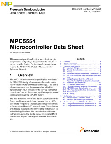
Electrical CharacteristicsTo avoid this condition, minimize the ramp time of the VDD supply to a time period less than the timerequired to enable the external circuitry connected to the device outputs.During initial power ramp-up, when Vstby is 0.6v or above. a typical current of 1-3mA and maximum of4mA may be seen until VDD is applied. This current will not reoccur until Vstby is lowered below Vstbymin. specification.Figure 2 shows an approximate interpolation of the ISTBY worst-case specification to estimate values atdifferent voltages and temperatures. The vertical lines shown at 25 C, 60 C, and 150 C in Figure 2 arethe actual IDD STBY specifications (27d) listed in Table 9.Figure 2. fISTBY Worst-case SpecificationsMPC5554 Microcontroller Data Sheet, Rev. 412Freescale Semiconductor
Electrical Characteristics3.7.1Input Value of Pins During POR Dependent on VDD33When powering up the device, VDD33 must not lag the latest VDDSYN or RESET power pin (VDDEH6) bymore than the VDD33 lag specification listed in Table 6, spec 8. This avoids accidentally selecting thebypass clock mode because the internal versions of PLLCFG[0:1] and RSTCFG are not powered andtherefore cannot read the default state when POR negates. VDD33 can lag VDDSYN or the RESET powerpin (VDDEH6), but cannot lag both by more than the VDD33 lag specification. This VDD33 lag specificationapplies during power up only. VDD33 has no lead or lag requirements when powering down.3.7.2Power-Up Sequence (VRC33 Grounded)The 1.5 V VDD power supply must rise to 1.35 V before the 3.3 V VDDSYN power supply and the RESETpower supply rises above 2.0 V. This ensures that digital logic in the PLL for the 1.5 V power supply doesnot begin to operate below the specified operation range lower limit of 1.35 V. Because the internal 1.5 VPOR is disabled, the internal 3.3 V POR or the RESET power POR must hold the device in reset. Sincethey can negate as low as 2.0 V, VDD must be within specification before the 3.3 V POR and the RESETPOR negate.VDDSYN and RESET PowerVDD2.0 V1.35 VVDD must reach 1.35 V before VDDSYN and the RESET power reach 2.0 VFigure 3. Power-Up Sequence (VRC33 Grounded)3.7.3Power-Down Sequence (VRC33 Grounded)The only requirement for the power-down sequence with VRC33 grounded is if VDD decreases to less thanits operating range, VDDSYN or the RESET power must decrease to less than 2.0 V before the VDD powerincreases to its operating range. This ensures that the digital 1.5 V logic, which is reset only by an ORedPOR and can cause the 1.5 V supply to decrease less than its specification value, resets correctly. SeeTable 6, footnote 1.MPC5554 Microcontroller Data Sheet, Rev. 4Freescale Semiconductor13
Electrical Characteristics3.8DC Electrical SpecificationsTable 9. DC Electrical Specifications (TA TL to TH)Spec1CharacteristicCore supply voltage (average DC RMS 2Input/output supply voltage (fast input/output)3Input/output supply voltage (slow and medium input/output)VDDEH3.05.25V43.3 V input/output buffer voltageVDD333.03.6V5Voltage regulator control input voltageVRC333.03
MPC5554 Microcontroller Data Sheet, Rev. 4 Freescale Semiconductor 3 2 Ordering Information Figure 1. MPC5500 Family Part Number Example Unless noted in this data sheet, all specifications apply from TL to TH. Table 1. Orderable Part Numbers Freescale Part Number1 1 All devices are PPC5554, r